AMAZON multi-meters discounts AMAZON oscilloscope discounts
EDITOR'S NOTE
At the time of completion of the preceding 14 Sections, which constituted the original manuscript of "Metallic Rectifiers, Principles and Applications," the use of silicon as the semiconductor in rectifiers was announced. In order to include information on silicon rectifiers, we have included this section which discusses the basic concepts of design and application of this new type rectifier. We wish to thank Mr. George Eannarino, Director of the Rectifier Division of Sarkes Tarzian, Inc., for his co-operation in making this information available.
Introduction
The silicon rectifier is a new development recently introduced in the field of power conversion and semiconductors.
The silicon rectifier exhibits several properties which make its future outlook perhaps brighter than the three types previously discussed.
The semiconductor properties of silicon have been known for many years. As early as 1904, point contact (cats whiskers) detectors made of silicon were used in radio receivers. With the advent of the vacuum tube, interest in the point contact detector decreased and it was not for many years that interest was again revived.
In the 1930's research workers began the study of shorter radio wavelengths. They found that ordinary vacuum tubes were of little use in this region and some new type of detector was needed. In the search for a new detector, the properties of the old point contact silicon detector were evaluated.
In an attempt to improve the old detectors, methods of producing purer silicon were developed. Improvements came rapidly and the silicon detector became a practical device, thus making radar practical during World War II.
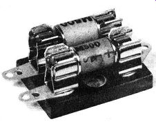
Fig. 15-1. The Sarkes Tarzlan M500 Silicon Rectifiers Being Used In Television
Receivers.
Through further experiments during and after World War II, the silicon transistor was developed in 1948. Continuing research lead to the introduction in 1956 of the silicon power rectifier which is shown in the photograph of Fig. 15-1.
Theory of Operation
Silicon, as used in silicon rectifiers, is a nearly perfect single crystal of pure metal to which has been added an element from either Group m or Group V of the Periodic Table. (Silicon is in Group IV.) Silicon doped with a Group m element conducts electrical current by means of holes, and is designated as "P" type. Silicon doped with a Group V element conducts current by means of electrons, and is designated as ''N" type. Actually, since the introduction of all undesired elements is impossible to control, there are both Group III and Group V elements present and the overall effect is that of the net difference. Thus, in ''N" type silicon, the difference in the number of Group V atoms minus the number of Group III atoms determines the number of conduction electrons. The most numerous carriers are designated as majority carriers; for example, electrons are majority carriers in ''N" type silicon and holes (positive charges) are minority carriers.
The silicon junction rectifier or diode consists of a "P"-''N" boundary within the lattice of a single crystal of silicon. In silicon area type rectifiers, the body of the wafer generally consists of "N" type silicon on which a very thin layer of "P" is formed by either alloying or diffusing a suit able material. The boundary or barrier layer thus formed is very thin, less than 10^-3 centimeters; therefore, on a junction capable of blocking a potential of 1000 volts, the space charge across the barrier layer is greater than 106 volts percenti meter. It is obvious, that to produce high voltage junctions, extreme care must be taken to eliminate all unwanted impurities that tend to ionize at high potentials.
At zero bias, diffusion effects of electrons and holes are opposed by an electrostatic space charge and the junction is at equilibrium; however, as an external voltage is applied, the junction exhibits unilateral characteristics of current flow. Current flows readily when a positive potential is connected to the "P" side of the junction, and very low currents flow when the potential is reversed. This unilateral effect defines the area of usefulness of a silicon rectifier, and the ratio of conductive to blocking resistance establishes the rectification ratio of the rectifier cell. Blocking resistances are as high as 10^9 ohms, while the forward resistances are measured in fractions of ohms; therefore, the rectification efficiency is greater than 99% with the forward drop contributing nearly the total loss.
Production of Silicon Rectifiers
Silicon does not readily lend itself to zone refining; therefore, the most popular methods to produce single crystals of pure silicon is crystal "pulling" where a seed of pure single crystal silicon is dipped into molten silicon, rotated slowly and withdrawn at a predetermined rate. A major problem in crystal "pulling" is to keep the resultant crystal free from contaminants. Molten silicon is very active and attacks the materials used in containers and holders. Quartz crucibles are commonly used and the entire process is conducted in an inert atmosphere to reduce the possibility of contamination.
Temperature is also very important and plus or minus 0.1° C. at approximately 1430° C. must be maintained.
When it is determined that the crystal has resulted in the desired type (either ''P" or ''N"), and that the resistivity is within the range that will produce suitable voltage ratings, the crystal is cut into thin slices and finally into small wafers or dice of desired size and thickness.
After suitable etching and grading to separate wafers that do not conform to established thickness specifications, the dice are alloyed by a special process. Alloying is conducted at high temperatures and provides not only a ''P"--''N" junction on one side of the wafer, but a low ohmic content on the base. Low resistance contacts are important, since once the internal space charge is overcome the resistance of the cell decreases exponentially and contact and lead resistances become factors limiting current flow.
Alloyed dice are brazed to a base and then hermetically sealed after a contact is provided to the alloyed side. Extreme care must be taken during the mounting and assembly operations to keep the surface free from contamination of any type since contaminants will ionize and shunt the junction.
Final electrical and mechanical tests are performed be fore and after successive heat cycles to make certain that the rectifier is stable under all conditions of temperature, humidity, altitude, and shock.
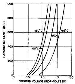
Fig. 15-2. Static Forward Current Vs. Applied Voltage.
Forward Characteristics
The direction of low resistance or high current flow is defined as the "forward" direction of the silicon rectifier, and since the majority of the power losses within the device are concentrated in the conduction cycle we will consider this care fully. Fig. 15-2 shows the classic static forward-current characteristics versus applied voltage. The curve of Fig. 15-2 shows that the effect of the space charge establishes a threshold voltage at approximately 0.6 volts DC. Note that once the device starts to conduct, the current increases exponentially with small increments of voltage and then increases nearly linear on a very steep slope.
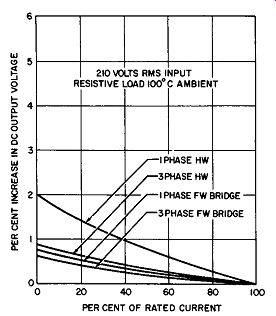
Fig. 15-3. Typical Regulation Curves for Various Circuits.
The current density of a silicon rectifier is very high and on present designs ranges between 600 and 750 amperes per square inch of effective barrier layer area. This depends to a great extent on the general construction of the enclosure and particularly on the ability of the heat sink to conduct heat from the crystal. A rectifier rated at one ampere DC and 15 amperes of peak surge current, contains a cell that has a total volume of .0000112 cubic inches. A rectifier rated at 15 amperes DC and 75 amperes of peak surge current, has a total cell volume of .000227 cubic inches. Peak currents are, therefore, extremely critical because the small mass of the cell will heat instantaneously and could conceivably reach failure temperatures within a time lapse of a few microseconds.
An increase in junction temperature increases efficiency as is shown by the curves of Fig. 15-2. Not only does an in crease in cell temperature cause a general forward resistance decrease, but a relative decrease of threshold voltage also occurs. This decrease is caused by an increase in thermal energy and agitation which, in turn, raises the energy level of the holes and electrons, thus reducing the space charge.
Typical regulation curves for various circuits are shown in Fig.15-3. The three-phase bri0 to 100%. The single-phase half-wave circuit is the least efficient with a change of 2% in output voltage as the load is varied from 0 to 100%.
Reverse Characteristics
The reverse direction of a silicon rectifier is characterized by extremely high resistance, up to 10^9 ohms, below avalanche voltage; at the avalanche voltage, a very sharp break occurs and the resistance rapidly decreases. This characteristic, graphically illustrated in Fig. 15-4, shows typical reverse current versus reverse voltage. Note the initially low values of reverse current and the sharp break as the critical voltage is reached. Because of this it is good practice to rate the peak inverse working voltage at least 20% below the avalanche point to provide a safety factor.
The avalanche point varies between rectifiers produced from the same crystal and depends to great extent on two factors: (1) The resistivity of the segment of crystal from which the wafer is cut, with crystal resistivity depending on distributed impurities within the crystal lattice; and (2) surface contamination introduced during alloying, brazing, assembly, or sealing. Contaminants will ionize at relatively low voltages and shunt the junction.
In a high voltage silicon rectifier that is virtually free of surface contamination and with uniform distribution of impurities, the avalanche is caused by ionization of atoms within the crystal and the junction assumes characteristics similar to those that apply to ionization of gases.
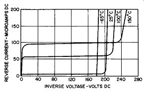
Fig. 15-4. Static Reverse Isothermal Curves for Sarkes Tarzian Type 15N
1 Silicon Rectifier.
Isothermal reverse curves are shown in Fig. 15-4.
These show that the avalanche voltage increases with an in crease in temperature and a general softening of characteristics is noted. The avalanche voltage decreases by about 10% between room temperature and extremely low temperatures; however, since 20% is allowed on initial rating, a safety factor is provided. At temperatures higher than room temperature the avalanche voltage increases; therefore, there is no need for derating.
Efficiency of the Silicon Rectifier
Reverse losses represent a negligible factor of power dissipation because of extremely low back currents. The forward losses, however, contribute very nearly the total loss within a silicon cell. To illustrate the magnitude of difference, a typical 600-volt rectifier will pass approximately 5 micro-amperes of back current at rated voltage for a back resistance of 120 megohms and a power dissipation of .003 watts. The same rectifier rated at one ampere DC connected in a single phase half-wave circuit, would have a forward voltage drop of 2.5 volts when operating at 100% rated current. The forward resistance of the cell would be 2.5 ohms and a power dissipation of 2.5 watts. In this case, the resistance ratio is approximately 120,000,000 to 1 and the forward to reverse power ratio is approximately 800 to 1. A rectifier rated at 600 volts peak inverse will deliver approximately 200 watts of power to a load, in a half-wave circuit, with internal losses of about 1 watt at an efficiency of 99.5%. This will become important as the fields of application extend to heavy current equipment.
Operating Temperatures
Silicon rectifiers are designed to operate in ambients from _550 C. to 1000 C. without derating and to 150° C. with moderate derating. The maximum case temperature is 170° C. with a 20° C. thermal gradient anticipated between the case and the cell.
Parallel Operation
Silicon rectifiers are produced as half-wave units with maximum current limits; however, at times it is necessary to use individual rectifiers in parallel to obtain sufficient output. Because the forward resistance is very low once a silicon rectifier starts to conduct, any unbalance between threshold voltages or internal voltage drop would cause serious unbalance of load distribution and ultimate failure of the overloaded section. For this reason it is recommended that a small series resistance be used with each half-wave section operating in parallel.
Series Operation
No special precaution is required when silicon rectifiers are operated in series, provided that the sum of the peak inverse ratings is not exceeded. Fig. 15-5 shows the effect of operating rectifiers with unbalanced peak inverse ratings. Note that each unit will increase until its individual avalanche point is reached; at this point, there is a leveling off regardless of how much the source voltage is increased.
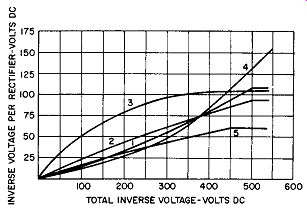
Fig. 15-5. Inverse Voltage Per Rectifier with Five Sarkes Tarzian "P" Type
Silicon Rectifiers Connected in Series.
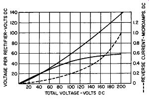
Fig. 15-6. Inverse Voltage Per Rectifier with Two Sarkes Tarzian "P" Type
Silicon Rectifiers Connected in Series.
Fig. 15-6 shows reverse current versus voltage with unbalanced rectifiers operating in series. This data shows there is no tendency for the reverse current to increase sharply even though the peak inverse ratings of individual rectifiers are exceeded.
Conventional Circuits
Silicon rectifiers are generally produced as half-wave units; however it is possible to connect single units into a variety of single phase and polyphase combinations.
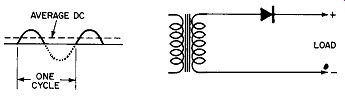
Fig. 15-7. Single-Phase, Half-Wave Rectifier Circuit.
Single-Phase, Half-Wave
It is not necessary to use more than one unit per circuit unless load requirements for voltage and current exceed the ratings of a single unit. When an input capacitor filter is used, it is necessary to provide a few ohms of surge limiting resistance to prevent rectifier failure. Also, the peak voltage rating of the rectifier should not be exceeded since the DC voltage contributes to the total back voltage. In the circuit of Fig. 15-7, a special transformer design is required because of core saturation effects of unidirectional current and high rms to DC ratios.
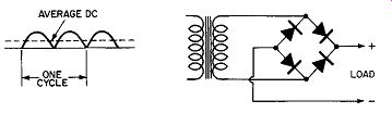
Fig. 15-8. Single-Phase, Full-Wave Bridge Type Circuit.
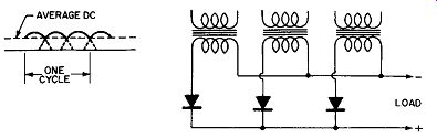
Fig. 15-9. Three-Phase, Half-Wave Rectifier Circuit.
Single-Phase, Full-WaveBridge
The circuit of Fig. 15-8 shows four half-wave silicon rectifiers used in a single-phase full-wave bridge circuit. Full wave output reduces ripple and increases efficiency.
Transformer design is simplified since both halves of the in put cycle are utilized. The transformer secondary voltage is approximately 1.25 times the DC output voltage.
Three-Phase, Half-Wave
Three single-phase, halt-wave silicon rectifiers are required to obtain a three-phase, half-wave circuit. See Fig. 15-9. Better circuit utilization provides relatively high efficiency and low ripple at three times the fundamental frequency. The output voltage is approximately equal to the phase voltage; however, the rms voltage rating of each arm of the rectifier must be equal to the line voltage which is 1. 73 times the phase voltage.
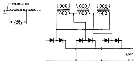
Fig. 15-10. Three-Phase, Full-Wave Bridge Type Circuit.
Three-Phase, Full-WaveBridge
The three-phase bridge circuit, shown in Fig. 15-10, requires six single-phase, half-wave units. This circuit delivers very high efficiency and is commonly used where DC power requirements are large. Due to overlapping of the three phases the ripple percentage is low, approximately 4%, and though additional filtering may be required, the resultant ripple that is six times the fundamental source frequency is easily filtered. The DC output voltage is approximately 25% higher than the input phase voltage.
Comparison of Output Voltages of Silicon Versus Selenium Rectifiers
A typical full-wave voltage doubler circuit, commonly used in television receivers, is shown in Fig. 15-11. The charts shown in the following, compare the output voltage of the silicon rectifier with that of the selenium rectifier, using values of 4.2 ohms and 5.2 ohms for the series resistor R1.
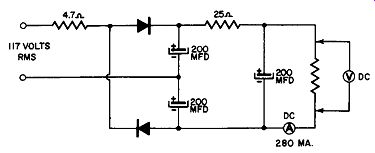
Fig. 15-11. A Typical Full-Wave, Voltage-Doubler Circuit.
SILICON RECTIFIER (SARKES TARZIAN M500) SELENIUM RECTIFIER (SARKES TARZIAN 300)
The Model M500 silicon rectifiers produced by Sarkes Tarzian, Inc. are designed primarily for use in television receivers where-voltage doubler circuits operating directly off the line are in common use. Their small size, high efficiency, and low cost make them desirable for use in all types of commercial electronic equipment.