AMAZON multi-meters discounts AMAZON oscilloscope discounts
Introduction
Now that the reader has become acquainted with the three types of metallic rectifiers and their properties as discussed in the preceding sections of this guide, he will want to learn how they may be employed. Although rectifiers are used in many types of applications involving control or measurement circuits, some of which will be described later, this section will deal exclusively with the primary purpose for metallic rectifiers--their use in circuits for conversion of AC to DC. There have been many rectification circuits which have been developed throughout the years; however, a number of these circuits have become standard practice for all types of applications. These circuits can be divided into three major groups as follows:
1. Single-phase rectification circuits.
2. Voltage-multiplier rectification circuits.
3. Three-phase rectification circuits.
In the succeeding sections of this section only the more useful rectification circuits in each group will be described.
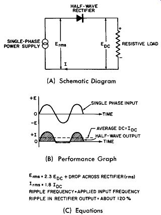
Fig. 9-1. A Single-Phase, Half-Wave, Rectifier Circuit.
Single-Phase Rectification Circuits
Single-phase rectification may be divided into the following four groups:
a. Single-phase, half-wave rectifier circuit.
b. Single-phase, half-wave circuit with capacitor.
c. Single-phase, full-wave center-tap circuit.
d. Single-phase, full-wave bridge circuit.
The circuits to be described in connection with these four groups are the most used in radio, television, light duty domestic, and industrial applications.
Single-Phase, Half-Wave Rectifier Circuit
This circuit is shown in Fig. 9-1A. In this figure a single-phase power source, for example the conventional 60 cycle source, feeds a simple series circuit consisting of a half wave rectifier and a resistive load. As far as AC to DC power conversion is concerned, the circuit of Fig. 9-1A is not an efficient or useful rectification circuit. A discussion of it, however, provides a convenient stepping stone to the more effective rectification circuits. Later in the guide the reader will encounter the principal use of this simple circuit in special control applications.
Fig. 9-1B shows that although a single-phase AC voltage is applied to the simple series circuit, the resulting current flow is practically unilateral; this current flow is represented by the shaded sinusoids directly below the portion of the input voltage waveform which causes the rectifier to conduct. Thus, during one half of the input cycle, current conduction takes place in the series circuit; while during the other half cycle, negligible current conduction takes place. During this latter cycle only the reverse or leakage current flows and we have learned from previous discussion that this reverse current may have a value somewhere between 1/100 to 1/1000 of the forward current. (In the case of the magnesium-copper sulfide rectifier this ratio may be about 1/25.) Because the current flows during only one half of the input cycle the arrangement derives its name "half-cycle" rectifier.
A DC ammeter in series with the rectifier and the resistive load will not respond to the rise and fall of the rectified current, if the applied frequency is about 50 to 60 cycles or higher. The meter will indicate the average rectified current flow in the circuit. The dashed horizontal line in the current waveform of Fig. 9-1B represents this average DC current value.
Since the rectified output is not a steady flow of direct current, it can be represented as a steady current with an alternating component super-imposed upon it. The frequency of the alternating component is the same as the applied frequency, that is, the ripple frequency in the rectified output is the same as that of the applied alternating input.
In Fig. 9-1C the significant equations for the circuit are given. The applied input voltage in root-mean-square, the value as read by an AC voltmeter, is equal to 2.3 times the DC voltage as measured across the resistive load plus the voltage drop across the half-wave rectifier in root-mean-square. The root-mean-square current drawn from the power source is equal to 1.8 times the value of the rectified current as indicated by a DC ammeter in series with the resistive load. The ripple component in the rectifier output is greater in magnitude than the steady current and in percent is about 120 to 125. This percentage is determined by the following equation:
Percent ripple
AC ripple voltage (rms) X 100%
Average DC voltage
Single-Phase, Half-Wave Rectifier With Capacitor
The single-phase, half-wave rectifier circuit of Fig. 9-1A becomes practical with the addition of one capacitor in shunt with the resistive load. This arrangement is illustrated in Fig. 9-2A. The circuit is quite similar to that described for Fig. 9-1A with the important addition of an electrolytic capacitor of large capacitance across the resistive load. A refinement consists of a limiting resistor is series with one line to protect the rectifier against excessive capacitor charging currents.
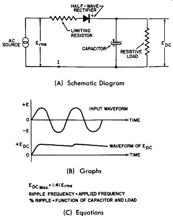
Fig. 9-2. A Single-Phase, Half-Wave, Rectifier Circuit With Capacitor. (A)
Schematic Diagram; (B) Graphs; (C) Equations
To describe the function of the electrolytic capacitor and why it improves the half-wave rectifier, consider first that the resistive load is temporarily removed. Connected as shown, the rectifier in this circuit conducts only when the upper AC input terminal is positive at which time the capacitor is charged to the peak value of the AC input voltage less the conducting voltage drop across the rectifier of about 5 volts for a radio type selenium rectifier rated at 130 volts rms.
That is, starting from an input voltage of zero value and letting this voltage increase sinusoidally in the positive direction to the peak level, the capacitor is charged substantially to this peak value of voltage also, because the forward resistance of the half-wave rectifier is small. When the input waveform decreases to zero, the capacitor keeps its charge because it cannot discharge through the half-wave rectifier in the reverse direction (assuming a perfect rectifier with zero leakage). When the load resistance is applied to this charged capacitor, and/ or when the rectifier is imperfect because of leakage current, current is withdrawn from the charged capacitor continuously, so each conductive cycle must make up the loss and the capacitor voltage rises and falls each cycle to a degree dependent upon the value of the capacitor in farads and the resistance of the load in ohms. The product of these two factors is called the time constant of the circuit and equals numerically to R x C where R is expressed in ohms and C is expressed in farads.
In this circuit, then, the ripple frequency is the same as the applied frequency and the percent of ripple is a function of the time constant and the output voltage level is a function of the load.
Fig. 9-2B graphically shows the waveform of the applied voltage and the waveform of the rectified output when a small amount of current is drawn from the charged capacitor. The output waveform starts from zero, at time equals zero, to illustrate the initial conditions when the circuit is first powered.
The first positive half-cycle charges the capacitor to peak value. Since current is being drawn from it because of the shunting resistive load, the voltage across the load decreases until the next positive half-cycle recharges the capacitor.
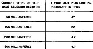
Fig. 9-3. Chart for Selecting Proper Peak-Limiting Resistor.
To limit the peak charging current to a safe value so as to protect the rectifier, it is necessary to connect a peak current limiting resistor of the appropriate size in series with the supply voltage as shown in Fig. 9-2A. Current flowing through this resistor produces a voltage drop across the resistor; rectifiers with higher current ratings will require less peak limiting resistance to produce a given IR drop. The value of this peak limiting resistor will depend upon the current rating of the rectifier used. It will range from 4 or 5 ohms for a rectifier rated at 500 to 1000 milliamperes to about 50 ohms for a rectifier rated at 50 milliamperes. The required wattage of the peak limiting resistor varies from 2 to 3 watts for the 50 milliampere rectifier to 5 watts for the 1000 milli ampere rectifier. Fig. 9-3 presents a chart showing the appropriate peak limiting resistor to use with a selenium half wave rectifier of a given current rating when this rectifier is used in the circuit of Fig. 9-2A. An important characteristic of any power supply is its voltage regulation. This refers to the amount by which the DC output voltage drops from its no-load terminal value to its value at full-rated output current. Voltage regulation is expressed as a percentage and is equal numerically to: where, Percent voltage regulation = 100% ( E1- E2 ) E2 E1 is the no-load terminal DC voltage.
E2 is the DC output voltage at full current drain.
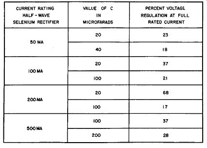
Fig. 9-4. Voltage Regulation Chart.
Best voltage regulation for the circuit of Fig. 9-2A is obtained when the capacitor across the load is a large value of capacitance in microfarads. An illustration of the function of this capacitor on the voltage regulation is given by the chart of Fig. 9-4 which shows the percent voltage regulation to expect for various values of capacitance, when using the half-wave selenium rectifiers listed, at their full-rated current values.
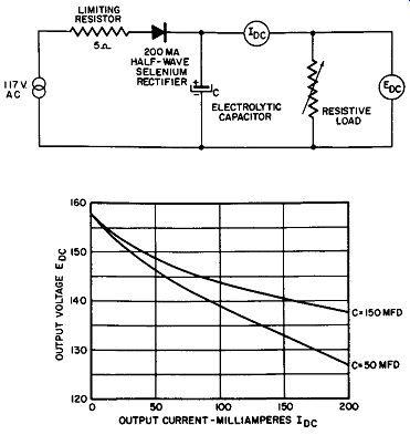
Fig. 9-5. Circuit and Voltage Regulation Curves for Half-Wave Rectifier
Circuit, With Capacitor.
Fig. 9-5 gives a practical adaptation of the half-wave rectifier circuit with capacitor using the selenium type of metallic rectifier, including circuit details and illustrating the effect of the value of the capacitor upon the rectified voltage output versus current delivered to the load--in other words, the voltage regulation of the circuit as a function of the shunting capacitor.
As neither the rectifier nor the electrolytic capacitor is "perfect", the rectified voltage at the zero load current value is not quite 1.414 times 117 volts AC. This peak value as shown on the graph is about 158 volts. The regulation of the circuit is better with the larger capacitor, for, at this value, the output falls but 21 volts for a current ranging from 0 to 200 milliamperes. When the shunting capacitor is reduced to 50 mfd, the voltage fall is 31 volts for the same load range.
One can see from Fig. 9-5 that the regulation of the circuit described is not excellent, yet in many cases this is not required, for, the load may be fixed. Moreover, because compact, inexpensive electrolytic capacitors are available with large capacitance ratings, this type of circuit serves well for small current requirements. Furthermore, it makes possible rectified output voltage equal to or greater than the applied line voltage at rms value without the use of a step-up transformer. This feature is popular for the AC-DC type of radio and TV receiver.
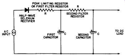
Fig. 9-6. Adding a Second Stage of R-C Filtering to the Half-Wave Rectifier
Circuit.
In the half-wave rectifier circuit with capacitor, a second stage of R-C (resistance-capacitance) as shown in Fig. 9-6 will augment the smoothing action of the ripple component of the DC output at the expense of poorer voltage regulation. It is desirable that the second capacitor have the same value of capacitance in microfarads as the first capacitor and that both have the same minimum DC working voltage ratings equal to the peak value of the applied AC supply voltage. The value of the resistor R is a function of the load and the output voltage required. The larger it is in ohms, the better will be the filtering action. A value of 100 to 1000 ohms is typical in some power supplies. When very low ripple is desired in the output, several identical filter stages may be cascaded.
Single-Phase, Full-Wave, Center-Tap Rectifier Circuit
We have seen that the half-wave rectifier circuit of Fig. 9-1A suffers from poor voltage regulation and excessive ripple voltage because the power is transferred from AC to DC only during half of the alternating cycle. To improve upon this performance, a capacitor was utilized in the second arrangement described to act as a flywheel during the non-conducting cycle of the half-wave rectifier and give up part of its electrical charge to sustain the steady flow of current. The better voltage regulation of this system is greatly dependent upon the use of large values of capacitance and, even then, the system is limited to rectified currents of small values, certainly not greater than one ampere and usually to currents of the order of a few milliamperes to about 500 milliamperes.
(A) Schematic Diagram (B) Graphs (C) Equations
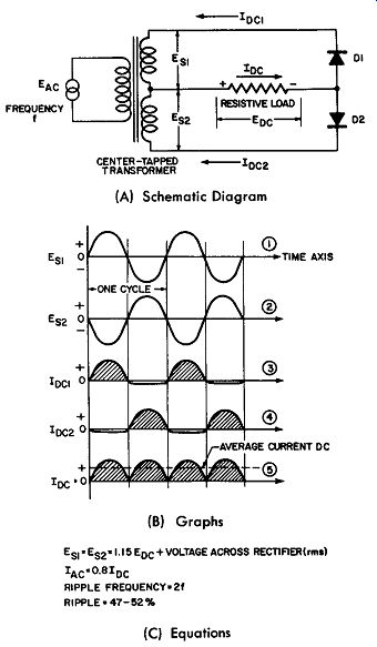
Fig. 9-7. A Single-Phase, Full-Wave, Center-Tap Circuit.
To improve this performance it is necessary to extract rectified power during both halves of the alternating input. This may be accomplished by the use of a center-tapped transformer and two half-wave rectifiers. The arrangement and the details are given in Fig. 9-7. The use of the center-tapped secondary on the transformer, coupling the rectifier circuit to the AC source, provides two equal and opposite voltages as referred to the center-tapped connection. These voltages are designated as Es1 and Es2. Their time and magnitude relationships are shown by the first two waveforms of Fig. 9-7B. The two half wave rectifiers, D1 and D2, and the common resistive load are connected as shown in Fig. 9-7 A and the arrangement provides a full-wave direct current delivery to the load because rectifier D1 delivers a half cycle of direct current on one alternation, while rectifier D2 delivers its equal share of current during the succeeding alternation. See Fig. 9-7B, waveforms 3 and 4, and then correlate waveform 3 with waveform 1 and waveform 4 with waveform 2. The current flow through the resistive load is the summation of IDC1 and IDC2 which equals IDC; this is shown graphically by waveform 5. The dashed line through this waveform represents the average value of the rectified current flowing through the load as indicated by a DC ammeter.
The equations of Fig. 9-7C illustrate that the secondary voltage required in rms is equal to 1.15 times the rectified voltage across the load plus the voltage drop across the rectifier in rms. The AC input in rms to the rectifier circuit proper equals 0.8 times the rectified current in the load. The ripple frequency of this circuit is double that of the input frequency; for a verification of this statement study waveform 5 with 1 in Fig. 9-7B. The percentage ripple is of the order of 47 to 52 percent.
Although this arrangement is better than the previous systems described because it is of the full-wave rectification type resulting in better voltage regulation, and lower ripple (more uniform DC output); the transformer design is not efficient as each half of the secondary still works half of the time.
Thus, this arrangement is most useful when full-wave rectification is required and the design is limited to two half-wave rectifiers; it is principally economical when low DC voltage is required--approximately 8 to 10 volts. Where the requirement for the DC output is greater than 10 volts, it is necessary to have two rectifiers in series where but one cell is shown in Fig. 9-7A. For this reason the center-tap circuit loses ad vantage when the output voltage requirement necessitates two half-wave rectifiers in each rectifier branch. When several rectifier cells must be used in series, the center-tap transformer design is no longer economical because of its half duty cycle and center-tap requirements. The choice then falls upon the single-phase, full-wave, bridge rectifier.
Single-Phase, Full-Wave Bridge Rectifier Circuit
(A) Schematic Diagram (B) Voltage and Current Waveforms (C) Equations
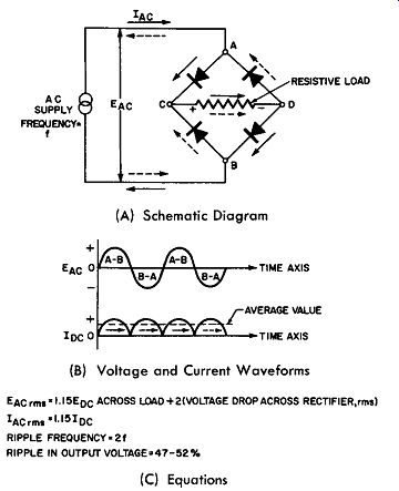
Fig. 9-8. A Single-Phase, Full-Wave, Bridge Rectifier Circuit.
The most popular single-phase rectifier which uses both rectifier and transformer components efficiently is the full wave bridge arrangement. Efficiencies of the order of 60 to 70 percent are obtained because both halves of the input cycle supply the load. The circuit is shown in Fig. 9-8A. It will be found that four half-wave rectifiers are connected in a manner to provide full-wave rectification. When the input alternation is such that terminal "A" of the bridge is positive and terminal "B" is negative, the direction of the resulting current flow is given by the solid arrows. When the alternation of the input voltage wave is such that junction "B" is positive and junction "A" is negative, the current flow direction is indicated by the dashed arrow lines.
It is important to note that although two sets of rectifiers are used, resulting in different paths for the current flow through the diagonals of the bridge for the positive and negative alternation of the input voltage, the direction of the current flow through the load is the same for both alternations providing full-wave power to the resistive load. These details are shown graphically in Fig. 9-8B, while Fig. 9-8C provides the necessary equations. See Section 3 of this guide for other details of the single-phase, full-wave bridge rectifier.
Voltage-Multiplier Rectification Circuits
This group of single-phase rectification circuits have such a unique property that they may be separately classified under the above title. This property of the circuits to be described is the ability to supply rectified or DC potentials exceeding the peak value of the applied alternating voltage and to achieve this greater voltage without the need for bulky, expensive, power transformers. Generally the higher voltage rating of these circuits requires the use of the selenium type of metallic rectifiers. In replacing the power transformer and the conventional rectifier tubes used, selenium metallic rectifiers have made available low cost, compact, light weight TV receivers. In one application, the TV chassis, redesigned to use metallic rectifiers in voltage multiplier circuits to obtain the required B+ voltage, weighs as little as the power trans former alone used in the previous design of the TV receiver providing the same operational characteristics.
Using the principles of the voltage multiplier rectification circuits, there is no theoretical limit to the maximum voltage which can be obtained; however, the most popular applications limit the use of these circuits to arrangements pro viding 3 to 4 times the peak value of the applied line voltage, or about 500 volts DC for a 117 volts, 60 cycle input.
Voltage multiplier rectification circuits which require the application of half-wave rectifier assemblies may be divided into five groups as follows:
a. Voltage doubler, half-wave.
b. Voltage doubler, full-wave.
c. Voltage tripler.
d. Voltage quadrupler.
e. Ladder Circuit.
(A) The Circuit
(B) Voltage Graphs
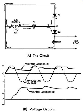
Fig. 9-9. A Half-Wave Voltage Doubler.
Half-Wave Voltage-Doubler Circuit
The voltage doubler, half-wave rectification circuit is the most frequently used transformerless voltage multiplier.
The no-load DC output voltage of this circuit is 2 x 1.414 or about 2.82 times the rms value of the AC supply voltage. Thus, a voltage doubler rectification circuit powered from a 117 volt AC line will deliver a no-load DC output voltage of approximately 330 volts, neglecting the voltage drop across the rectifiers in its circuit. As output current is drawn, the DC voltage will fall; this decrease of output voltage is a function of the DC load and the value of the capacitors of the circuit.
The half-wave voltage doubler circuit is shown in Fig. 9-9A. By examining the circuit, the reader can determine that it consists of a series loop comprising two half-wave rectifiers D1 and D2 and an electrolytic capacitor, C2. The rectifiers are connected in series additive, that is, the positive terminal of D1 is connected to the negative terminal of D2.
Since it is customary to use polarized electrolytic capacitors in these circuits for reasons of economy, the proper connection for C2 is to connect its positive terminal to the positive terminal of rectifier D2 as shown.
The positive terminal of the first capacitor C1 is connected to point m at the junction of the two rectifiers. The alternating voltage power supply has one terminal B connected to the remaining terminal of the electrolytic capacitor C1, while its other terminal A is connected to the junction between rectifier D1 and the negative terminal of electrolytic capacitor C2.
The principle of operation of this circuit will be under stood by the reader by following the circuit performance for one alternation of the AC input. First, assume that portion of the input alternation in which terminal A of Fig. 9-9A is positive with respect to terminal B of the AC supply. For this condition of the circuit rectifier D1 will be conductive and rectifier D2 will be non-conductive and charging current will flow in the direction shown by the solid arrows to charge capacitor C1 until it assumes a voltage equal to the peak potential of the line. (In this case this will be 1.414 x 117 volts.) In the next half cycle, as terminal B becomes positive with respect to terminal A, the charge of capacitor C1 will add its potential to that of the peak value of the AC supply voltage and the current flow will be through rectifier D2 (this current flow is indicated by the dashed arrows) charging capacitor C2 to a potential equal to that of the peak line voltage plus the voltage across C1. The voltage across C2 is thus equal to twice the peak line voltage--at no load. The load, of course, is applied across C2. Under this load, capacitor C2 recharges but once during a complete alternation of the AC input, so the ripple frequency is the same as the line frequency and the voltage regulation of the system is poorer than that obtained from the full-wave voltage doubler to be described next.
In Fig. 9-9B the upper portion of the voltage graph shows in dashed lines the sinusoidal waveform of the applied AC input.
During the positive alternations, rectifier D1 conducts and charges capacitor C1; during the negative alternations the charge in C 1 partially discharges into C2, accounting for the fall of potential shown by the solid line curve marked "voltage across C1". During the negative alternation of the AC input, rectifier D2 conducts and the charge of C1 plus the line voltage in additive fashion charge C2 to approximately twice the peak value of the applied line voltage. The resultant voltage waveform, for a light load across C2, is shown by the lower solid line curve of Fig. 9-9B.
Although the voltage regulation and the ripple frequency of the half-wave voltage-doubler circuit is inferior to the full-wave voltage-doubler circuit to be described, it is the circuit more widely used because one terminal of the rectified output is common to the AC input source tending to reduce AC hum and stray pickup problems because this common junction between input and output may be grounded.
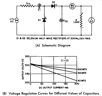
Fig. 9-10 A Practical, Half-Wave, Voltage-Doubler. Rectifier Circuit. (A)
Schematic Diagram; (B) Voltage Regulation Curves for Different Values of
Capacitors.
In a practical circuit the two rectifiers used are identical as are also the two capacitors. Capacitor and rectifier polarities must be observed. The voltage regulation of the circuit is improved by use of large capacitance values for the two capacitors. For example, when using half-wave rectifiers of the selenium type rated at 200 ma, 130 volts rms, the voltage regulation is about 50 to 60 percent when the capacitors have a value of 40 microfarads and 20 to 30 percent when the capacitors are increased to 100 microfarads.
Fig. 9-10 gives a practical, half-wave voltage-doubler, rectifier circuit with typical component values. The voltage regulation graph shows the performance to be expected for different values of capacitances. The function of the 5 ohm resistor is to act as a limiting resistor to the initial current surge while the capacitor is being charged and to act as a fuse in the event that a short circuit occurs in the DC load.
Full-Wave Voltage-Doubler Circuit
The full-wave voltage-doubler circuit is shown in Fig. 9-11A. It involves the same number of components as the half wave voltage-doubler circuit discussed previously but the arrangement and performance are different. In this circuit the outer loop consists of two rectifiers and two capacitors. The two rectifiers, connected in series additive (positive terminal of one to the negative terminal of the other), are wired in series with the two capacitors also connected in series additive.
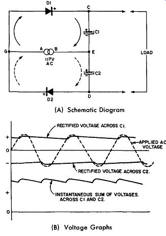
Fig. 9-11. A Full-Wave Voltage-Doubler Circuit.
Terminal A of the AC power supply is wired to the junction between the two rectifiers (see junction G) and terminal B is wired to junction E between the two capacitors. The load for the rectified voltage is applied across the two capacitors C1 and C2.
The principle of operation of this circuit is as follows: When terminal A of the AC supply voltage is positive with respect to terminal B, current flow represented by the solid arrows passes through rectifier D1 and charges C1 to peak line voltage with point C positive with respect to junction E. In the next half-cycle, when terminal B of the AC source be comes positive with respect to terminal A, capacitor C2 is charged (represented by the current flow line shown by the dashed arrows) so that terminal D is negative with respect to junction E. At no-load then, the rectified output potential across terminals C to D is twice the peak line voltage at the end of a full cycle of alternation. With no-load then, the rectified output voltage across the two capacitors is equal to 2.82 times the AC supply voltage measured in rms. With load the capacitors lose part of their charge during the cycle and the output voltage is a function of load current and the rating of the capacitors in farads.
Fig. 9-11B graphically presents the applied AC voltage (in dashed waveform), the resulting rectified output voltage waveforms across C1 and C2, and the instantaneous summation of the voltage waveforms across C1 and C2, as seen by the load.
One can see that the capacitors in this full-wave circuit are charged alternately on each cycle of the AC input and then discharge additively into the load. For this reason the full-wave voltage-doubler has better voltage regulation and a lower ripple component in the rectified output than the half-wave voltage doubler circuit.
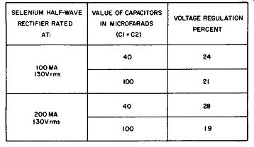
Fig. 9-12. Voltage Regulation Characteristics of the Full-Wave Voltage Doubler.
The chief disadvantage of the full-wave voltage-doubler circuit is that neither output terminal can be "grounded" for neither output terminal is common to the AC terminals. AC hum and stray pick-up will be a greater problem when using this type of power supply with sensitive amplifiers and receivers but this difficulty is partly offset by the lower ripple component and the better voltage regulation.
The chart of Fig. 9-12 illustrates the voltage regulation to expect from the full-wave voltage-doubler circuit at two half-wave rectifier ratings and for two values for the capacitors; identical capacitors and rectifiers are used for each respective circuit.
(A) Schematic Diagram; (B) Voltage Regulation Graph
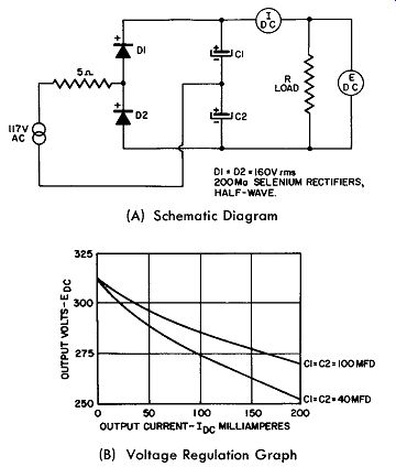
Fig. 9-13. A Practical Full-Wave, Voltage-Doubler Rectifier Circuit.
Fig. 9-13 gives a practical circuit which employees the full-wave voltage-doubler principle. The accompanying graphs show the voltage regulation to expect at various loads up to the rating of the rectifier. In this circuit, polarities of the rectifiers and the electrolytic capacitors must be observed and C1 and C2 must be equal. The current and voltage ratings of the half-wave rectifiers, D1 and D2, should also be equal.
The familiar peak limiting resistor is also included.
The Voltage-Tripler Circuit
The voltage-tripler rectifier circuit is a transformer less voltage-multiplier which has a no-load DC output equal to three times the peak applied AC voltage or 3 x 1.414 or 4.242 times the rms value of the AC supply voltage. When this circuit is powered from a conventional 117 volt AC power line, the no load DC output voltage will be approximately 496 volts if the potential drop across the rectifiers is neglected. When the output terminals are loaded, the DC voltage will decrease as a function of the load and the size of the capacitors used.
Three identical rectifiers and three identical electrolytic capacitors are employed in the voltage-tripler circuit.
The larger the capacitors the better the voltage regulation of this circuit.
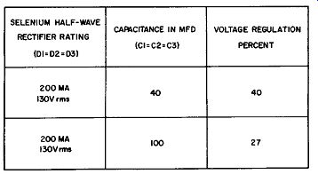
Fig. 9-14. Voltage Regulation Chart for Voltage Tripler Circuit.
This function of the capacitors in the voltage-tripler circuit is shown by the chart of Fig. 9-14 which shows what may be expected for two values of capacitors in a tripler circuit using three selenium half-wave rectifiers rated at 130 volts rms, 200 milliamperes.
To understand the circuit and principle of operation of the voltage-tripler rectifier arrangement, consider first the half-wave voltage-doubler circuit of Fig. 9-9A and confirm that it can be redrawn as shown in Fig. 9-15A.
The principle of operation of this circuit which was discussed previously can be extended to higher orders of voltage multiplication. The voltage across C2 can be added to a succeeding rectifier-capacitor stage to provide an output voltage which is equal to three times the peak value of the applied line voltage and, if desired, this latter capacitor voltage can be added to still another rectifier-capacitor stage and so on until the desired voltage multiplication is achieved.
Fig. 9-15B shows the schematic diagram of the half wave, voltage-tripler as an extension of the half-wave, voltage doubler circuit of Fig. 9-15A. The dashed lines in Fig. 9-15B show the rectifier-capacitor stage which was added.
(A) Half-Wave Voltage-Doubler Circuit; (B) Voltage-Tripler Circuit
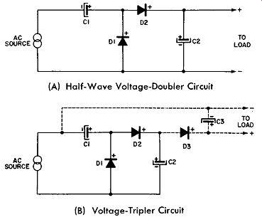
Fig. 9-15. The Development of the Half-Wave, Voltage-Tripler Circuit.
(A) Schematic Diagram; (B) Voltage Regulation Curves
Fig. 9-16. A Practical Voltage-Tripler Circuit.
The schematic diagram of the practical half-wave voltage-tripler rectification circuit is given in Fig. 9-16A, while Fig. 9-16B shows the voltage regulation curves for two values of circuit capacitors. Again the polarities of the electrolytic capacitors and the half-wave rectifiers must be ob served and the capacitors must be equal and so must the rectifiers. By comparing the circuit of Fig. 9-16A with Fig. 9-15B the reader can verify that the arrangements shown are equivalent electrically.
The Voltage-Quadrupler Circuit
As an extension of the principle discussed in the fore going, that is, by adding rectifier-capacitor stages in the proper manner, the voltage multiplication factor of the circuit may be advanced to any practical level desired. Fig. 9-17 shows the half-wave voltage-quadrupler rectification circuit which results when one additional rectifier-capacitor stage is added in the proper manner to the voltage-tripler circuit of Fig. 9-16A.
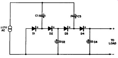
Fig. 9-17. A Voltage-Quadrupler Rectification Circuit.
This circuit is especially useful for low-powered electronic equipment; a study of the circuit shows that it simply comprises two half-wave voltage doubler rectification circuits in series. This circuit delivers a no-load, DC terminal output voltage equal to 4 x 1.414 times therms value of the AC supply voltage. Thus, a voltage-quadrupler rectification circuit operating from a 117 volt AC power line will deliver a no load DC output voltage of about 660 volts. As output current is drawn, the DC output voltage will decrease to a value dependent upon the load and the size of the circuit capacitances.
Four identical rectifiers and four identical capacitors are required for this circuit and the polarities must be observed.
The voltage regulation of this circuit employing four half-wave selenium rectifiers rated at 130 volts rms, 200 ma and four capacitors at 40 mfd is about 89 percent; when the capacitors are increased to 100 mfds, the voltage regulation is about 36 percent.
(A) Schematic Diagram; (B) Voltage Regulation Curves
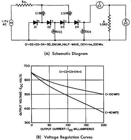
Fig. 9-18. A Practical Voltage-Quadrupler Rectification Circuit.
Fig. 9-18 shows the details of a practical voltage quadrupler rectification circuit with voltage regulation curves.
Yet another means to obtain a voltage-quadrupling rectification circuit is to connect two half-wave voltage-doubler circuits similar to that shown in Fig. 9-15A with the AC input circuits in parallel and the DC output circuits in series additive. The circuit diagram for this arrangement is drawn in Fig. 9-19. Again the no-load DC output voltage is 4 x 1.414 times therms alternating current input voltage. With an input of 117 volts AC, the DC output voltage at no load is equal to approximately 660 volts when the potential drop across the rectifiers is neglected.
The voltage regulation of this circuit is 85 to 90 percent when the capacitors are identical and equal to 40 mfd; when the capacitors are equal to 200 mfd, the voltage regulation is 35 to 40 percent. The rectifiers are all identical and rated at 130 volts rms, 200 ma, selenium, half-wave.
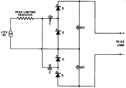
Fig. 9-19. Another Voltage-Quadrupling Scheme.
The Ladder Circuit
Another circuit powered from the single phase AC source provides voltage multiplication in its DC output. The configuration of this circuit's diagram provides it with its fancy name of the Ladder voltage multiplier circuit. This voltage multi plier rectification circuit provides a multiplier factor which is a function of the number of rectifier-capacitor stages.
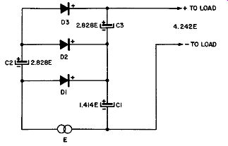
Fig. 9-20. The Ladder Voltage Multiplier Circuit.
The diagram of the circuit is given in Fig. 9-20, which shows a three stage arrangement to provide a DC output voltage which is equal to 3 x 1.414 times therms value of the AC input.
In this circuit the capacitors may progressively decrease in capacitance with the distance from the AC source. The current ratings of the half-wave rectifiers may also be de creased in the same fashion.
In operation if we can assume that each capacitor is very large in comparison with the capacitor in the succeeding stage then the first half cycle of alternation charges C1 to 1.414E. In the next half cycle of alternation C2 is charged to 2.828E; and finally in the third half cycle of alternation C3 charges to 3 x 1.414E or 4.242E. In succeeding cycles of alter nations the voltages across these capacitors are maintained.
It can be seen, then, that the voltage of C1 is additive to that of C3 making the DC output voltage as seen by the load 3 x 1.414E. The multiplication factor of the ladder circuit can be extended with additional rectifier-capacitor stages to obtain enormous DC potentials from the primary 117 volt AC line.
Such high voltage power sources are very useful for X-ray and cathode-ray equipment.
Three-Phase Rectification Circuits
Three-phase rectifier circuits are but an extension of the single-phase rectification circuits already studied. These three-phase circuits are chiefly used for heavy current applications in which the better efficiency and the lower ripple component become important. The higher efficiency and the lower ripple component in the three-phase circuit results be cause each phase contributes current in turn only while the applied voltage is near the peak value. For this reason, in a three-phase rectifier circuit capacitors or filter circuits are not needed to achieve smoothness of rectified output which cannot be approached by single-phase circuits without the use of such auxiliary components.
Of the large number of three-phase rectifier circuits devised, this guide will only deal with the following more useful ones:
a. Three-phase, half-wave rectifier circuit.
b. Three-phase, full-wave center-tap rectifier circuit.
c. Three-phase, full-wave bridge rectifier circuit with Y connected AC source and Delta connected AC source.
d. Three-phase, full-wave rectifier circuit with inter-phase or balancing transformer.
Three-Phase, Half-Wave Rectifier Circuit
This circuit is similar in principle to the single-phase, half-wave rectifier circuit previously discussed. The improvement in the performance of the three-phase circuit over that of the single-phase circuit is due to the overlapping of the three-phase rectified current, resulting in an output current throughout the entire cycle. The ripple frequency is three times the applied frequency of the power source and its magnitude is held to about 18 percent.
(A) A Three-Phase, Half-Wave, Rectifier Circuit Connected Direct to Y Connected Source.
(C) Equations
(B) A Transformer-Coupled, Three-Phase, Half-Wave Rectifier Circuit.
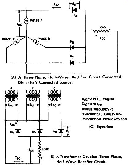
Fig. 9-21. The Three-Phase, Half-Wave, Rectifier Circuit.
Fig. 9-21 gives the pertinent facts about this circuit.
Fig. 9-21A represents the schematic diagram of the circuit when the power is obtained directly from a Y connected power source. Fig. 9-21B represents the schematic diagram of the circuit when the power is obtained from the secondary of trans formers whose primaries are connected to a three-phase power source of either the Y or delta type; and Fig. 9-21C gives the more important formulas for the circuits shown.
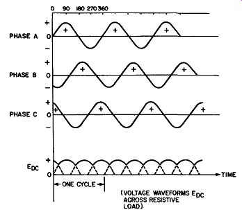
Fig. 9-22. Waveform Graphs for Three-Phase, Half Wave, Rectifier Circuit.
(A) Schematic Diagram; (B) Output Voltage Waveform Across Resistive Load; (C) Formulas
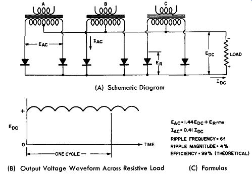
Fig. 9-23. A Three-Phase, Full-Wave, Center Tapped Rectifier Circuit.
Fig. 9-22 shows graphically the voltage waveform of the three-phase input and the resultant waveform of the output voltage across a resistive load.
Three-Phase, Full-Wave, Center-Tap Rectifier Circuit
This circuit is derived from the single-phase, full-wave center-tap circuit and is particularly useful when heavy rectified currents at low voltage are required. A center-tap on each phase winding of the coupling transformer secondary is required. The complete details are shown in Fig. 9-23.
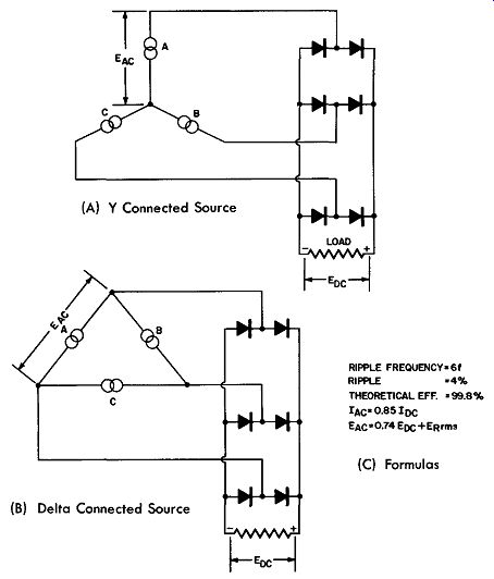
Fig. 9-24. The Three-Phase, Full-Wave Bridge Rectifier.
(A) Y Connected Source; (B) Delta Connected Source; (C) Formulas
Three-Phase, Full-Wave, Bridge Rectifier
The three-phase, full-wave bridge rectifier circuit is one of the most useful and economical circuits for heavy rectified current requirements. It has a high theoretical efficiency of 99 percent and the rectified output contains only 4 percent of ripple component. The frequency of this ripple is six times the applied frequency.
This circuit can be used without coupling transformers when the line voltage is of the proper level and the resulting DC output across the resistive load is approximately the same as the AC voltage supply level. Either a delta or a Y connected power source may be used. The details are shown in Fig. 9-24.
Three-Phase, Full-Wave Rectifier With Inter-Phase Transformer
Fig. 9-25 represents a three-phase, full-wave rectifier circuit with an inter-phase or balancing transformer connecting the two sets of secondary circuits. Without this trans-former, the circuit becomes a standard six-phase connection and the current conduction occurs during 1/6 of the cycle; with the inter-phase transformer included in the circuit as in Fig. 9-25, the current conduction period is increased to 1/3 of a cycle, thus increasing the current rating of the rectifier output.
(B) Formulas
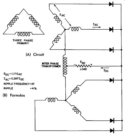
Fig. 9-25. A Three-Phase, Full-Wave, Rectifier Circuit With Inter Phase
Transformer.