AMAZON multi-meters discounts AMAZON oscilloscope discounts
The silicon controlled rectifier (scr) is a semiconductor that is cap able of providing efficient control of large amounts of a-c and d-c power. It is rapidly finding application in various types of power supply circuits. The basic operation of the silicon controlled rectifier is explained in the following paragraph.
FIG. 1 aids in the basic understanding of the SCR structure since the two transistors are equivalent to one SCR. The two transistors are positioned back to back; the collector of transistor Q1 (an NPN unit) is connected to the base of transistor Q2 (a PNP unit), and the collector of Q2 is returned to the base of Q1. A meter placed in series between the emitter of Q2 and the supply voltage indicates current through the NPN-PNP combination. When there is no input current applied to the base of Q1, the meter indicates only a slight leakage current through the NPN-PNP pair. Note that the current applied to the gate lead ( the base current of Q1 ) is multiplied by the beta ( amplification factor) of Q1, and this becomes the base current of Q2.
The base-emitter current of Q2 in turn is amplified by the beta of Q2 and fed back to the base of Q 1. When there is an input current the betas of Q1 and Q2 increase until their product is greater than unity.
At this point the current from Q2 exceeds the input current applied to the base of Q1. Regeneration causes the current through Q1 and Q2 to increase until both transistors are in a current-saturated condition.
The meter then indicates a maximum current in the circuit. The important characteristic of the NPN-PNP combination is that, below a certain point, there is only a slight current through them. However, when sufficient current is available at the gate terminal, they snap into conduction almost instantaneously. As a result, this combination resembles a snap-action on-off switch-either passing no current or a maximum current, with no in-between state. This is in contrast to a conventional transistor amplifier, where the current may be smoothly varied from zero to maximum.
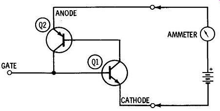
FIG. 1. Transistor equivalent of a silicon controlled rectifier.
The practical SCR does not consist of two separate transistors.
Rather, it is made up of a sandwich of alternate P-type and N-type semiconductor materials, as shown in FIG. 2A. Note how this corresponds to the equivalent SCR circuit in FIG. 1. The electronic symbol for the SCR is shown in FIG. 2B. FIG. 2C shows the characteristic curve of a typical SCR. If no current is applied to the SCR gate electrode (IG = 0), the SCR will not conduct until the forward breakover voltage (IG = 0) has been reached. At this time, the semiconductor will conduct heavily. If the anode current is reduced below the minimum holding current, the SCR will revert to its nonconducting state.
When a current is applied to the gate electrode (IG1 or IG2), the effect is to decrease the forward breakover voltage. This is indicated by the three curves, each of which represents a progressively higher value of gate current. The gate current can be increased to the point where the SCR has forward-current characteristics very similar to those of a conventional semiconductor diode. In a sense the SCR can be considered a form of current amplifier because a small value of gate current can control a large anode current. It is also important to note that once the gate triggers the SCR into conduction, the gate loses all control over anode current. Reducing the gate current to zero, or even making it negative with respect to the cathode, will not cut off the anode current.
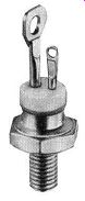
-------- Courtesy Tung-Sol Electric Inc. A 16-ampere silicon controlled rectifier having a peak reverse-voltage rating of 960 volts.
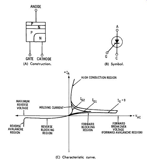
FIG. 2. Silicon controlled rectifier. (A) Construction. (B) Symbol. (C)
Characteristic curve.
TYPICAL SCR CIRCUITS
The SCR is strictly an "on-off" device; variation in output is achieved by changing the length of the on and off times. Special techniques must be employed to utilize the SCR in power-supply circuits.
Phase Control
One of the most common methods used to vary the turning on and off of scr's is phase control. FIG. 3 illustrates the basic phase-con trolled SCR power supply. The SCR is arranged in a simple half-wave rectifier circuit with the gate connected to a phase-shift network which is capable of varying the phase difference between the gate and anode of the SCR from O to 180 degrees. When the phase-shift network is adjusted for a zero-degree phase difference between the SCR gate and anode, the SCR will conduct during the entire half-cycle that the anode is positive, as indicated in FIG. 4. If there is a 90-degree phase difference between the SCR gate and the anode, the SCR conducts for one half of the half-cycle, as indicated in FIG. 4B. Increasing the phase difference between the SCR gate and anode to 180 degrees keeps the SCR from conducting ( FIG. 4C). The output voltage of the power supply is determined by the average amount of power delivered to the load. This can be changed by varying the phase of the signal applied to the SCR gate.
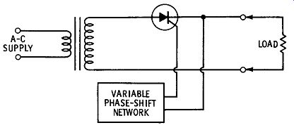
FIG. 3. Phase control of the SCR supply.
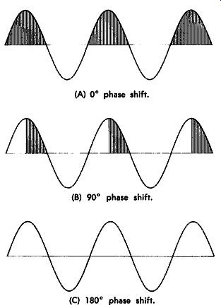
FIG. 4. Load waveform in an SCR circuit. (A) 0° phase shift. (B) 90° phase
shift. (C) 180° phase shift.
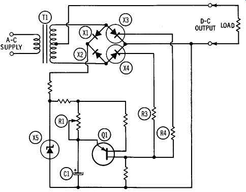
FIG. 5. SCR power supply with voltage control.
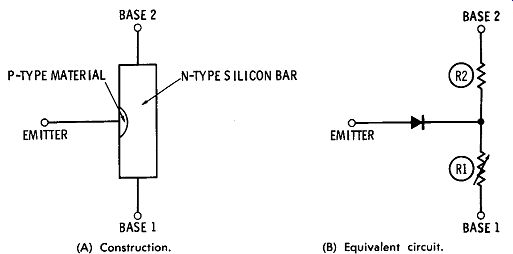
FIG. 6. Unijunction transistor. (A) Construction. (B) Equivalent circuit.
Unijunction Transistors
FIG. 5 shows a typical full-wave SCR power supply incorporating a unijunction transistor in the phase-control circuitry. Before the circuit can be analyzed, however, the operation of a unijunction transistor (ujt) must be understood.
Basically, the ujt is constructed of a piece of N-type silicon with ohmic (non-rectifying) contacts at each end, as illustrated in Fig. 6A. A P-type rectifying contact, called the emitter, is formed on one side in the middle of the N-type material. The N-type silicon material acts like a simple resistive voltage divider with a diode tied into its center. Refer to the equivalent circuit, FIG. 6B. FIG. 7 shows the electrical characteristics of the ujt. When no current is applied to the emitter junction and a positive voltage is applied to base two, the voltage-divider action of the resistive N-type silicon material places a small reverse bias on the emitter junction.
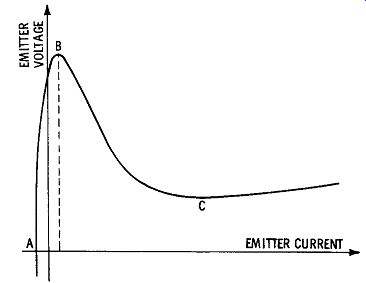
FIG. 7. Characteristic curve for a ujt.
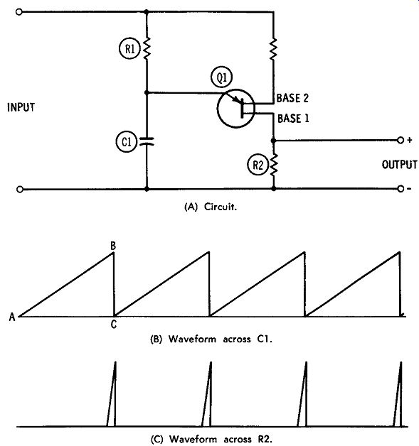
FIG. 8. Basic ujt relaxation oscillator.
(A) Circuit.
(B) Waveform across C1.
(C) Waveform across R2.
As a result, there is only a small reverse current in the emitter circuit.
This is represented at point A in FIG. 7. As the forward bias applied to the emitter junction is increased, there is a decrease in the emitter reverse current, as indicated by the region between points A and B in FIG. 7. When point B is reached, the P-N junction becomes forward biased; forward emitter current starts and the resistance between the emitter and base one drops to a very low value. Since the emitter voltage decreases as the emitter current increases, a negative-resistance characteristic results, as indicated between points B and C in FIG. 7.
Take a look at FIG. 8A, which shows the unijunction transistor used in a relaxation-oscillator circuit. When an input voltage is first applied to the circuit, capacitor C1 acts like a short circuit, so the emitter is at ground potential. Because of the voltage-divider action of the silicon material, there is a positive voltage at base one, and the base-one-emitter junction is reverse biased. As capacitor C 1 charges, the voltage across it can be represented as the line between points A and B in FIG. 8B. At point B the voltage is sufficient to forward-bias the emitter. The emitter junction now conducts, making the effective emitter-base-one resistance drop to a very low value. Capacitor C1 rapidly discharges through this low resistance, as indicated by the line between points B and C in FIG. 8B. When capacitor C1 is discharged, the whole cycle starts over again.
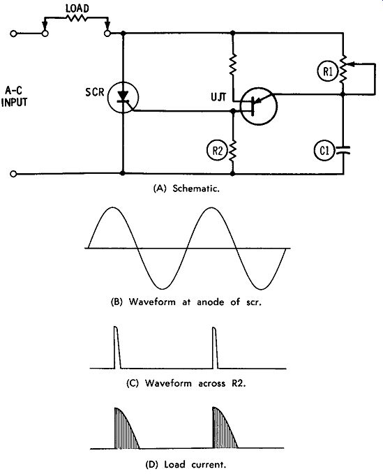
FIG. 9. Ujt phase control.
(A) Schematic.
(B) Waveform at anode of SCR.
(C) Waveform across R2.
(D) Load current.
FIG. 8C shows the voltage pulses developed across resistor R2 each time C 1 discharges through the forward-biased emitter junction.
The frequency of the output pulses can be changed by varying the value of resistor R1. For a given value of C1, reducing the value of R1 will increase the frequency, and vice versa.
FIG. 9A shows how a ujt can be used as the phase control in an SCR power supply. The ujt is connected as a relaxation oscillator with R1 as the charging resistor and C1 as the capacitor being charged. R1 is adjustable so the charging rate of C1 may be varied. The positive going pulses developed at base one of the ujt are applied to the gate of the SCR. In operation, as the positive half-cycle from the a-c input begins to increase in amplitude, the anode of the SCR becomes increasingly positive with respect to the cathode, as shown in FIG. 9B. At the same time the voltage applied to the ujt and the timing circuit R 1-C1 is also increasing. When the voltage applied to the ujt emitter has risen to a point sufficient to forward-bias it, C1 discharges through the low-resistance emitter junction, developing a positive-going pulse across resistor R2, as shown in FIG. 9C. This pulse, applied to the gate of the scr, turns the SCR on, and it conducts. There is current in the load for the portion of the positive half-cycle indicated in FIG. 9D. During the following half-cycle, the SCR anode is negative so it will not conduct. As a result, current will be applied to the load only on positive half-cycles of the a-c input.
FIG. 10 shows the same operating conditions as FIG. 9 except that resistor R1 has been adjusted to charge C1 faster. This results in C 1 discharging through the ujt emitter junction earlier in the positive half-cycle of operation, as shown in FIG. 10B. The SCR is turned on earlier in the cycle ( FIG. 10C), and the SCR will apply a greater portion of the positive half-cycle to the load. Thus, the point in the positive half-cycle at which the ujt fires determines the point at which the SCR conducts. Since the timing of the ujt capacitor discharge, in turn, is determined by the value of the charging resistor, the power applied to the load by the SCR can be easily controlled by varying the ujt charging resistor.
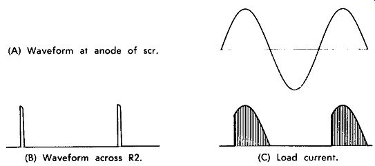
FIG. 10. Accelerated trigger. (A) Waveform at anode of SCR. (B) Waveform
across R2. (C) Load current.
Now return to the power-supply circuit of FIG. 5. The voltage appearing across the secondary of power transformer T1 is applied to diodes X 1 and X2, which are connected to form a full-wave rectifier. Although at first glance the presence of the scr's X3 and X4 suggests a bridge-rectifier configuration, they form a second full-wave rectifier for applying d-c power to the load.
The positive half-cycles from X1 and X2 are applied to the ujt circuitry; R1 and C1 form the charging network, with R1 being made variable to vary the charging rate of C1. The positive-going pulses at base one of the ujt are applied to the gates of the two scr's via isolating resistors R3 and R4. These pulses switch on the scr's on alternate half-cycles of operation. The SCR which has a positive anode at the time of application of the pulse from the ujt will conduct current to the load. By varying R1, the voltage control, the point in the cycle in which the ujt discharges may be varied, thus controlling the portion of the cycle in which the particular SCR will conduct. Zener diode XS stabilizes the voltage conditions under which the uni-junction transistor works in order to provide consistent operation.
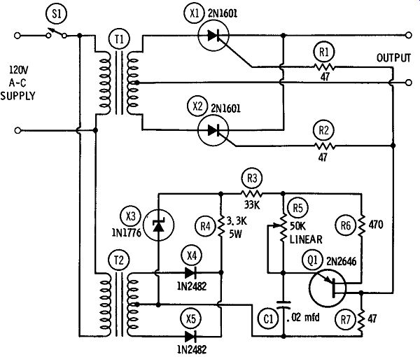
FIG. 11. Variable-voltage SCR power supply.
------------------- Parts List for FIG. 11
Item No. Description
C1
R1 R2 R3 R4 RS R6 R7
S1
T1 T2 X1 X2 X3 X4 X5
Q1
Capacitor, .02 mfd, mylar
Resistor, 47 ohms, ½ watt
Resistor, 47 ohms, ½ watt
Resistor, 33K ohms, ½ watt
Resistor, 3300 ohms, 5 watts
Resistor, variable, 50K ohms, linear
Resistor, 470 ohms, ½ watt
Resistor, 47 ohms, ½ watt
Switch, spst
Transformer, power, 40 volts center-tapped, 1200 ma (Stancor P8196, or equivalent)
Transformer, power, 120 volts, center-tapped, 50 ma (Knight 54D3708, or equivalent)
Rectifier, silicon controlled, 2N1601
Rectifier, silicon controlled, 2N1601
Diode, zener, 1N1776
Rectifier, silicon, 1N2482
Rectifier, silicon, 1N2482
Transistor, unijunction, 2N2646
------------------------
A PRACTICAL SCR POWER SUPPLY
FIG. 11 is the schematic of an scr-controlled variable-voltage power supply capable of providing from O0 to 40 volts at a current of up to 1 ampere. The circuit is essentially the same as the one shown in FIG. 5, except that a separate ujt power supply is used.
When the output voltage of this supply is low, the output ripple will increase considerably. The reason for this is that at low voltage levels, only a small portion of the half-cycle is passed on to the load. Thus, there will be relatively wide gaps between successive output pulses.
As a result, this supply is not recommended for loads requiring very low ripple.
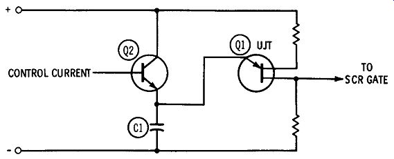
FIG. 12. Transistor control of ujt discharge rate.
REGULATED POWER SUPPLIES
Voltage-regulated power supplies using scr's have an advantage, in that these circuits dissipate very little power. In an all-transistor regulated supply, the current passed to the load is controlled by either a series or shunt control transistor whose effective internal resistance is varied by means of a control signal. The resistance of the control transistors represents a power loss ( transistor heating). On the other hand, an SCR in a regulated power supply is either in a state of full conduction or no conduction. When it is in full conduction, the SCR has almost zero internal resistance and so dissipates little power. This, of course, means good efficiency. It boils down to the fact that, on an equal power-output basis, the scr-regulated power supply may use much smaller semiconductor devices, both electrically and physically.
How Scr Voltage Regulation Is Achieved
To understand the basic operation of SCR voltage regulation, take a look at FIG. 12. Notice that this is the same basic ujt phase control described earlier except for the addition of transistor Q2, inserted in place of the charging resistor. This transistor is an electronically variable resistor, the effective resistance of which may be adjusted by controlling the base current. Thus, as the base current of Q1 is increased, the effective emitter-collector resistance will be decreased, and vice versa. Since the charging rate of C1 depends on the value of the charging resistor, it is easy to see that the charging rate of C1, and hence the firing rate of the ujt, can be controlled by transistor Q1.
Therefore, the firing rate of the ujt can be controlled by varying the base current applied to Q1 because this varies its effective internal resistance.
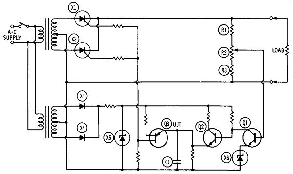
FIG. 13. Regulated power supply.
FIG. 13 illustrates an SCR voltage-regulated power supply using the transistor-controlled ujt principle just described. The base of Q1 is connected to voltage divider R1-R2-R3, placed across the output terminals of the supply. When the voltage across the external load increases, the base of Q1 becomes more positive with respect to its emitter since the latter is held at a constant voltage by zener diode X1. This increases the collector current of Q1, so the collector be comes less positive. Since the collector of Q1 is direct-coupled to the base of Q2, the base also becomes less positive with respect to the Q2 emitter. This decreases the collector current, thereby increasing the effective internal resistance. Since the emitter-collector circuit of Q2 forms part of the capacitor-charging circuit for the ujt, the increased resistance of Q2 decreases the charging rate of C1, and hence, the firing frequency of the ujt. As a result the scr's conduct later in their operating cycle, decreasing the average current applied to the load.
The load voltage will drop to its original value.
A decrease in load voltage has exactly the reverse effect. The effective resistance of Q2 decreases, the ujt fires sooner, and the scr's will conduct earlier in their cycle. This increases the average current applied to the load, bringing the load voltage back up to normal.
Other SCR Circuits
In addition to the SCR power-supply and voltage-regulator circuits described thus far, the SCR finds many additional applications. FIG. 14 shows how a single SCR can control the entire output of a full wave bridge. Using this circuit the power applied to the load can be varied from 0 to 100%. Note that the SCR (Q2) is in series with the load, so it is in a position to exercise complete control.
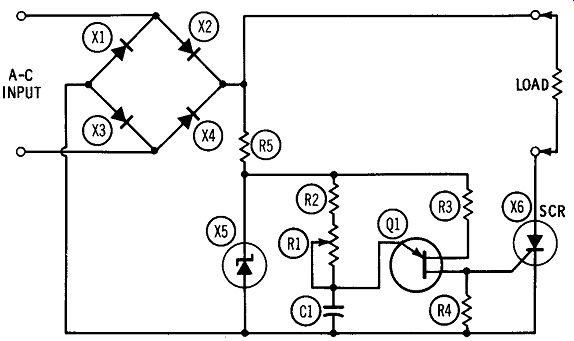
FIG. 14. Control of bridge rectifier.
The output of bridge rectifier X1, X2, X3, and X4 is a series of pulses; these are applied to both the load circuit and the trigger circuitry for the SCR gate. Capacitor C1 is charged by current through R2 and R1. At a certain emitter voltage, unijunction transistor Q1 fires, and the resulting pulse across R4 triggers the SCR. The SCR then conducts until the end of that pulse from the bridge. By adjusting control R1 the charging time of capacitor C1 can be changed so the SCR will conduct more or less of each half-cycle. Zener diode XS stabilizes the operating conditions of the trigger circuitry in order to obtain consistent performance.
CONTROLLED A-C SWITCHES
In order to control both halves of the a-c cycle, it is necessary to use either a single SCR in the output of a full-wave bridge rectifier ( FIG. 14), or two scr's that alternately switch the output of a full wave rectifier ( FIG. 5). Also, two scr's may be connected "back to back" to achieve full-wave control, although this generally requires two isolated phase-control circuits.
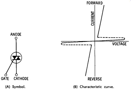
FIG. 15. Controlled a-c switch (triac). (A) Symbol. (B) Characteristic
curve.
In contrast, the controlled a-c switch ( triac) permits the relatively simple full-wave control of power. Basically, the triac consists of two "back-to-back" scr's with a common gate electrode, as shown schematically in FIG. 15A. The electrical characteristics of the triac are shown in FIG. 15B. When connected in series with a load in an a-c circuit, the triac may be triggered into conduction during alternate half-cycles to obtain full-wave control, since its anodes become alternately positive with respect to the common gate during alternate applied half-cycles.
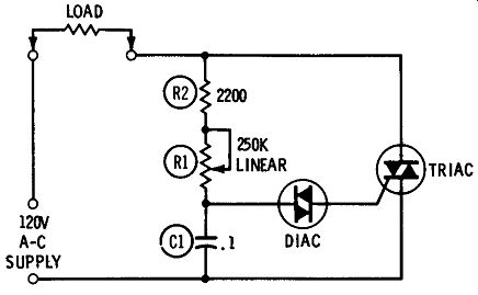
FIG. 16. Triac control circuit.
FIG. 16 shows a practical triac circuit. This provides full-wave power control and will handle loads up to 100 watts. The triac is phase-controlled by a relaxation oscillator consisting of the diac (negative-resistance diode), R1, R2, and C1.
The discharge rate of the relaxation oscillator is determined by setting the power control, R1. Unlike the ujt relaxation oscillator, however, the diac provides a gate trigger pulse from either negative or positive half-cycles.