AMAZON multi-meters discounts AMAZON oscilloscope discounts
All electronic components are resistive to some extent. However, resistive components as such are defined as those in which the resistive parameter is predominant. Typical resistive components are carbon-composition and wirewound resistors, potentiometers, vacuum tubes, crystal diodes, transistors, thermistors, voltage-regulator tubes, neon bulbs, thyratrons, and audio transformers. Fixed resistors and potentiometers are obviously resistive components. On the other hand, beginners tend to overlook the fact that a vacuum tube is also a resistive component. The distinction is simply this: a composition resistor is a passive device, whereas a vacuum tube is an active device.
VACUUM TUBES
A vacuum tube is classified as a resistive component because the heater has resistance and in addition, a vacuum diode has a plate resistance in typical operation. The diode may have a plate resistance from 600 ohms to infinity, depending on the plate voltage that is applied. A triode also has a plate resistance, and, in addition, it has a grid-input resistance that is very high unless the tube is defective. A tetrode also has a screen-grid resistance. These resistances are of basic concern in tube testing. Of course, a tube also has capacitance ; a vacuum diode has plate (interelectrode) capacitance, and a triode has grid input (interelectrode) capacitance. The capacitance parameters are less prominent than the resistance parameters in most situations; hence, a vacuum tube is usually regarded as a resistive component.
SEMICONDUCTORS
Transistors, likewise, are essentially resistive components. A transistor can be regarded in the first analysis as two crystal diodes connected back-to-back. Note that the term transistor implies the words transfer and resistance. These resistances and their variations under different applied voltages are of basic concern in transistor testing. Transistors also have junction capacitances; however, the junction capacitances are usually of secondary significance, and the transistor is regarded as a resistive component.
GASEOUS COMPONENTS
Crystal diodes are essentially resistive components. A crystal diode has junction capacitance that is ordinarily neglected.
However, you will find some applications in which the junction capacitance is of basic concern, and the diode resistance is neglected. That is, the junction capacitance is utilized as an electronic capacitor, inasmuch as the capacitance varies with the applied voltage. Such a semiconductor capacitor may be used as an FM modulator in a sweep-frequency generator. In this case, the crystal diode is not regarded as a resistive component, but as a capacitive component.
Gaseous components are classified as resistive because this parameter is usually of basic concern in applications and test procedures. A neon bulb has a practically infinite resistance or a low resistance of a few hundred ohms, depending upon the applied voltage. A voltage-regulator tube is a resistive component in the same general class as a neon bulb ; however, the design of voltage-regulator tubes is elaborated for the purpose of maintaining as constant a voltage drop as possible across the anode resistance in the conducting state. Thyratrons are resistive components in which the anode resistance has two discrete values (extremely high and very low) which can be switched from high to low by the grid-driving voltage.
TRANSFORMERS
Beginners often challenge the classification of an audio output transformer, for example, as a resistive component.
Because the conventional symbol shows two coil windings, the beginner assumes that the transformer has an inductive characteristic. This misconception, in the case of an audio output transformer, stems from a limited knowledge of electronic theory. In normal application, the transformer is loaded by a resistive utilization device, and its purpose is to match the source resistance (such as the plate resistance of a tube ) to the load resistance. Now, unless the transformer is defective, the load resistance will be reflected back to the primary terminals as a much higher and almost pure AC resistance--the tube does not "see" an inductive load. Hence, in the nature of things, an audio output transformer must be logically classified as a resistive component.
AC AND DC RESISTANCE
The newcomer is certain to confuse AC resistance with DC resistance. As a matter of fact, their values are often widely different. Consider an ordinary tuning coil in a broadcast receiver-its DC resistance is very low, but at 1 mhz its AC resistance will be much greater. This difference is due to skin effect in wires at higher frequencies, which forces the RF current out of the center of the wire and increases the apparent resistance. Furthermore, there are eddy-current losses in the wire, which imposes loss and increases the apparent resistance as the operating frequency is raised.
With this introduction to the subject of resistive components, the technical details of resistance must now be considered briefly, along with a breakdown into the chief forms of resistance and the way in which Ohm's law applies to each.
POSITIVE, NEGATIVE, AND ZERO RESISTANCE
Resistance occurs chiefly in three forms: positive, negative, and zero. An ordinary wirewound resistor exemplifies positive resistance. Negative resistance is found in oscillators, some types of amplifiers, and in all regenerative circuitry. The simplest negative-resistance component is the tunnel diode; but even an ordinary germanium diode, such as the IN34, becomes a negative-resistance component when it is suitably biased.
Zero resistance often is unrecognized; if you increase the back bias on a germanium diode, there is a critical voltage at which the diode has zero resistance-on one excursion from this point the diode has positive resistance, and on the other excursion, it has negative resistance.
Zero Resistance in the Laboratory
Sophisticated types of scientific equipment (including certain computer devices) utilize a type of zero resistance called super conductivity. Many metals which have positive resistance at room temperature suddenly develop zero resistance near absolute zero (-273 C). In other words, some ordinary conductors can become superconductors at very low temperatures.
Resistance and Ohm's Law
Ohm's law holds for all forms of resistance. This law states that I = E/R. In this expression, R is positive, and the formula says that the positive resistance opposes current flow. Again, if a component has negative resistance, Ohm's law is written I = E/-R. This formula states that the negative resistance enhances current flow. Otherwise stated, negative resistance increases current flow, whereas positive resistance decreases current flow. Finally, if a component has zero resistance, Ohm's law is written I = E/O.
The component neither opposes current flow nor enhances current flow. For example, if a current is started in a zero-resistance component, the same current theoretically will be found flowing in the component years later.
Zero resistance then, can be compared to the absence of friction in a mechanical device.
The Meaning of Resistance
Resistance, as defined by Ohm's law, is basically a voltage/current ratio. A graphical presentation of positive resistance is shown in Fig. 1. This relation shows that the current flow doubles when the voltage is doubled. Of course, this is an ideal, theoretical relation that is not strictly true in practice. However, if you make this test with an ordinary 100 ohm, wirewound resistor, the relation will seem to be true.
For many practical purposes, it can be said that a wirewound resistor is an ideal positive resistance. Although when substantial current is passed through the resistor, the electrical picture presented in Fig. 1 will be incorrect.
Coefficient of Resistance
Getting down to the practical details, it will be observed that the current flow does not exactly double when the voltage is doubled. When the current is made large enough to heat the resistor appreciably, this fact becomes quite .obvious. Metals have a positive temperature coefficient of resistance. This means that their resistance rises when the temperature is increased. Fig. 2 shows the electrical picture of a 7-watt, 117-volt lamp. The E/I characteristic is curved. It rises fast at low voltage, and rises less rapidly at higher voltages for which the resistance is higher.
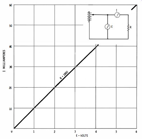
Fig. 1. An "electrical picture" of resistance.
Nonlinear Resistance
It follows that Fig. 2 depicts positive nonlinear resistance.
You will find that a composition resistor is also nonlinear and that it has a positive temperature coefficient of resistance.
If an ohmmeter is connected to a composition resistor as depicted in Fig. 1-3, and the pigtail is heated with a soldering gun, the pointer will creep up on the ohmmeter scale. But if the heat is removed and a chill spray is applied to the resistor, the pointer then creeps down the scale to its normal "cold" value.
Of course, if the resistor is greatly overheated, it becomes damaged and does not return to its initial resistance value.
RESISTANCE TESTS
The temperature coefficient of composition resistors is controlled in production, and various types are rated, for example, for 0.25, 0.5, or 1 watt of power dissipation. The power dissipated by a resistor is equal to PR, or E^2/R, watts. A composition resistor is customarily rated for a resistance change of less than 6% when operated at the full rated load. However, a thermally unstable resistor might change 300/0 in value from ambient to normal operating temperature. Moreover, its hot resistance can tend to drift up and down instead of stabilizing at an abnormally high value. In turn, associated trouble symptoms may be caused in TV receiver circuitry, such as rolling picture, fluctuating sound, loss of horizontal sync, variations in picture height, etc.
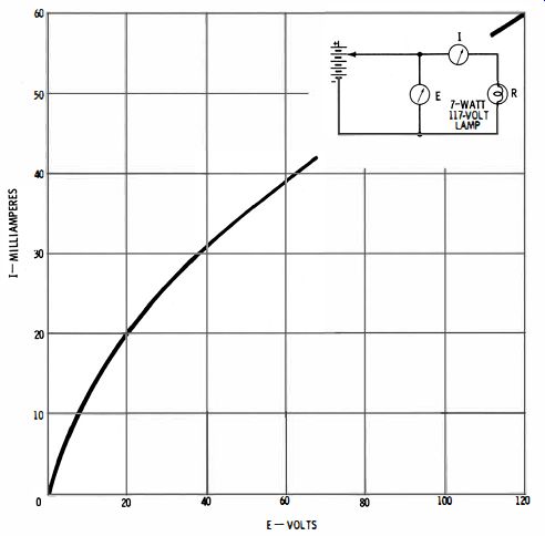
Fig. 2. An "electrical picture" of filament resistance.
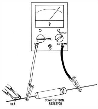
Fig. 3. Resistance increases with increase in temperature.
Testing For Thermal Stability
Hence, it can become necessary to check a suspected resistor for thermal stability, as well as its resistance value at an arbitrary, prevailing temperature. An out-of-circuit test can be made as depicted in Fig. 3. In addition to heating the resistor up to, or somewhat above, its normal operating temperature, it is also advisable to tap the resistor sharply while observing the ohmmeter reading as a mechanically unstable condition might be present.
Technicians commonly make in-circuit tests of resistors for thermal stability. In this case, the receiver or other device under test is used as an indicator, instead of an ohmmeter. For example, suppose that a picture-rolling symptom is to be localized. The grid resistors in the vertical-oscillator section are ready suspects. They can be heated with a soldering gun and then cooled with a chill spray, to see whether the rolling symptom is responsive. Potentiometers such as the vertical hold control are equally suspected in such a case and can be tested similarly.
To summarize the foregoing, it is clear that because ohm meter current does not overheat the resistor an ohmmeter is a practical instrument for measuring the nominal resistance values of wirewound and composition resistors. On the other hand, it is useless to use an ohmmeter to measure the resistance of a 1R5 tube filament because the ohmmeter current heats the filament substantially, and the current flow is unknown. Two different ohmmeters can be expected to read different values of filament resistance, and neither value is likely to agree with the rated resistance of the filament.
Resistance at a Point
It follows that the method depicted in Fig. 2 must be used to measure filament resistance. The rated voltage must be applied to the filament, and the current flow read for this applied voltage. To continue the previous example, a 1R5 tube has a rated filament-current flow of 0.05 ampere at 1.4 volts.
Ohm's law states that the resistance is 28 ohms for this voltage and current :
R = E/I = 1.4/0.05 = 28 ohms.
This is the resistance at the rated operating point and at some other operating point, the resistance value will be different. Far from being only an interesting theoretical fact, this has a very practical significance. In a series filament string, a tube that has higher than rated filament resistance will "rob" the other tubes. In the past, this has caused numerous "tough dog" service problems, and has resulted in the design of tube types which have closer tolerances on filament or heater resistance.
Operation of Series Heater String
Fig. 4 depicts a typical series heater string. Evidently, if all the tubes had comparatively high heater resistance, less than the rated 600-ma current flow would be measured in the circuit. However, if all tubes had comparatively low heater resistance, more than the rated 600-ma current flow would occur.
Too little current produces a subnormal operating temperature-emission goes down, and the local oscillator might "drop out," for example. Again, too much current produces an excessive operating temperature that can shorten tube life.
If you suspect a bad tube in a series string, it can be easily localized with an AC voltmeter. For example, you would expect to measure 12 volts rms across V7 (Fig. 4) , but if you measure a substantially higher voltage, the heater resistance is too high. In turn, you will find more or less sub-normal voltages across the other heaters-provided that they are not far out of tolerance.
Tube testers of the mutual-conductance type often provide a filament-activity switch or equivalent to determine whether a tube will operate satisfactorily at reduced heater voltage. A Gill reading is made with the heater voltage reduced approximately 1070. If the pointer falls in the "bad" sector during the filament-activity test, many technicians reject the tube without question.
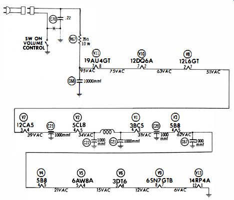
Fig. 4. A typical series heater string.
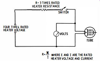
Fig. 5. Test setup for checking heater warm-up time.
Heater Warm-Up Time
Since there is a thermal lag when the line voltage is suddenly applied across a series string, it is desirable that the tubes heat up at about the same speed. There is a heavy starting current surge, as implied by the curve in Fig. 2. Tube life is prolonged by controlled heater warm-up time. This is defined as the elapsed time for the voltage across the heater to reach 8070 of rated value in the test circuit of Fig. 5. Note that the heater is energized through a series resistance having three times the rated heater resistance. The source voltage is four times the rated heater voltage.
The warm-up time can be measured with a watch having a sweep-second hand. It is the elapsed time from the instant the switch is closed to the moment that the voltmeter reads 807c of its final value. Note that the particular value of the warm-up time is not of significance in itself-the important consideration is whether all tubes in a certain heater string have approximately the same warm-up time. From previous discussion, it is clear that when one tube in a string has a comparatively slow warm-up time, it will cause abnormal voltages across other tubes in the string.
Although it is helpful to utilize tubes that have the same warm-up time, series strings are often protected also against the large starting-current surge (which still exists, although partially controlled ) by use of tubes with controlled warm-up time. This additional protection may be a series resistor having a negative temperature coefficient, as explained subsequently.
Or, it may be a relay-type of surge resistor as depicted in Fig. 6. When connected in series with a heater string, the device provides a high initial resistance which is later reduced to a very low value as the bimetallic blade closes the relay contacts.
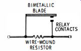
Fig. 6. Relay-type surge resistor.
Test of Surge Resistor
To test this component, first measure the resistance of the wirewound resistor (Fig. 6) with an ohmmeter. When the device is cold, the contacts are normally open, and the reading should be about 100 ohms. If you observe a very high resistance reading, the wirewound resistor (or its terminal connections) is defective. Conversely, if the resistance is very low, look for welded contacts or foreign matter between the contacts.
It is more difficult to check out the bimetallic blade because its cold resistance is normally about 0.1 ohm. However, if you have an ohmmeter with an R x 0.1 range, you can easily check the resistance of the bimetallic blade. A high reading indicates a defective element-one of the blades might be fractured, or it could have a resistive connection to its fixed terminal.
Finally, hold the relay contacts together, and measure the contact resistance ; it should be zero as indicated on the R x 0.1 ohmmeter range. If the contact resistance is measurable, clean the contacts with fine emery cloth.
The question may be asked why the bimetallic blade has a normal cold resistance of 0.1 ohm. The reason for this value is that the relay contacts must be held closed by J2R heating of the blade. Note that heat from the 100-ohm resistor closes the contacts initially. Then current flow is bypassed around the resistor by the bimetallic blade. Normal current flow dissipates sufficient heat in the 0.1-ohm resistance to warp the blade and keep the contacts closed.
NEGATIVE TEMPERATURE COEFFICIENT
Components with a negative temperature coefficient of resistance are widely used in electronic equipment. The difference between positive and negative characteristics is seen by comparing Fig. 7 with Fig. 8. A positive temperature co-efficient means that the resistance increases as the temperature (voltage ) is increased. On the other hand, a negative temperature coefficient means the resistance decreases as the temperature (voltage) is increased.
Depending on the point of view, the characteristic of a component having a negative temperature coefficient of resistance can be depicted in three different ways, as shown in Fig. 9. In other words, current may be plotted against voltage, resistance may be plotted against voltage, or resistance may be plotted against current. All three characteristics in Fig. 9 give the same information-they are simply tied together by Ohm's law.
Source of Negative Temperature Coefficient
Resistance is basically opposition to electron flow. If a substance has zero resistance, the moving electrons encounter no opposition. A metallic wire has many free electrons, which means that the electrons are comparatively unopposed while drifting from the negative end to the positive end of the wire.
Nevertheless, the conduction electrons strike a metal atom occasionally, as well as the other electrons that are given a random motion by heat energy. These collisions establish the resistance of the wire. Now, if the temperature of the wire is increased, the random motions of the electrons are increased, causing more collisions and consequently a higher resistance.
Hence, metals have a positive temperature coefficient of resistance.
However, semiconductors do not conduct by means of free electrons only. In addition to the electrons, holes are present.
Both electrons and holes conduct current. Now, the number of free electrons and holes that are present in a semiconductor is not the same at different temperatures. Instead, an increased temperature causes the production of more holes and free electrons. Since more current carriers become available in the presence of heat, the resistance decreases. Hence, semiconductors have a negative temperature coefficient of resistance.
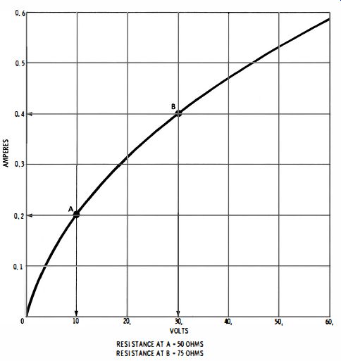
Fig. 7. Curve for positive temperature co-efficient of resistance.
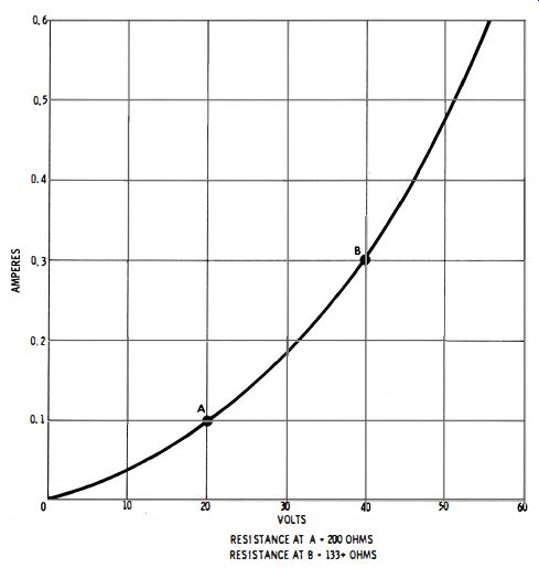
Fig. 8. Curve for negative temperature coefficient of resistance.
Ohmmeter Measurement
If you connect a thermistor to an ohmmeter as depicted in Fig. 10 and apply heat to the pigtail with a soldering gun, you will see the pointer falling on the scale. The more the thermistor is heated, the lower its resistance becomes. Note that the curves in Fig. 9 result from the generation of heat due to power dissipation in the semiconductor. Since power is equal to PR, a greater current flow generates more heat and reduces the resistance.
Sometimes a thermistor (also called a GLOBAR resistor) , is connected in a series heater string, instead of a wirewound resistor. Thus, a thermistor might be used instead of R67 in Fig. 4. A typical unit has a cold resistance of 130 ohms and a hot resistance of 31 ohms. In any case, the normal hot and cold resistance values will be specified in the receiver service data. Two ohmmeter measurements are usually adequate to check a thermistor. The chief precaution is to measure the hot resistance immediately after the power is switched off, so that the thermistor does not have time to cool.
Thermistors usually increase in resistance when they become defective due to aging. This can cause a slow warm-up of the receiver, even if other trouble symptoms do not result from the low heater voltage. Substantial increase in hot resistance results in a wide range of trouble symptoms, in addition to slow warm-up. In a typical case history, a ten-minute warm-up was required to obtain a full raster and brightness. The culprit was a heater-string thermistor that had a hot resistance of 50 ohms instead of 19 ohms.
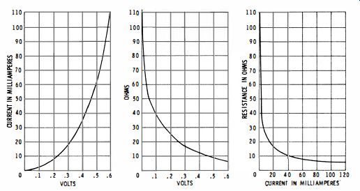
Fig. 9. Three methods of presenting negative temperature coefficient.
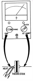
Fig. 10. Resistance decreases as the thermistor is heated.
Testing Small Thermistors
Comparatively small thermistors are used in low-current circuits, such as the plate-supply lead of a vertical oscillator.
Their cold resistance can be measured accurately with an ohm-meter. However, the hot resistance of a small thermistor does not lend itself to direct measurement. By the time the power has been switched off and the ohmmeter leads have been clipped to the thermistor, its temperature has usually dropped enough to result in a false reading.
Hence, accurate hot-resistance measurements require checking the thermistor with power on, in terms of voltage and current. Voltage drop across the component is readily measured with a VTVM, and the easiest way to calculate the current is to measure the voltage drop across a known resistor in series with the thermistor. Referring to Fig. 11, if 100 volts is measured across the I-meg resistor R71, the current through it (according to Ohm's law) is 0.1 ma. Then, if the voltage across thermistor R70 measures 50 volts, the hot resistance is 500K.
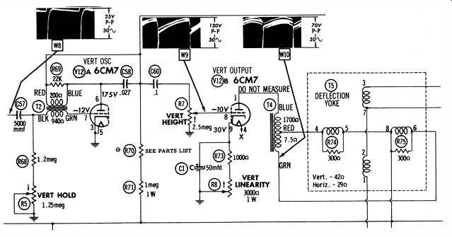
Fig. 11. Thermistor R70 stabilizes height and linearity.
SEMICONDUCTOR DIODES
If you measure the resistance of a thermistor, and then reverse the ohmmeter leads, the reading is the same. However, when this test is made on a semiconductor diode, widely different resistance values are normally obtained. The resistance readings shown in Fig. 12 are typical for the silicon junction diodes used in small power supplies. This ohmmeter test is only a rough indication of diode condition ; however, it also provides a ready means of establishing the terminal polarity of an unmarked diode.
Temperature Coefficient
While making either of the tests depicted in Fig. 12, you will observe that the resistance decreases if the diode is heated.
Even the heat transferred by holding the diode between your fingers will cause the pointer on the resistance scale to fall.
In other words, a semiconductor diode has a negative temperature coefficient of resistance. This temperature dependence is illustrated for a typical diode in Fig. 13A.
In practice, the temperature characteristic of semiconductor diodes is put to use in various ways. For example, germanium diodes are used to stabilize the emitter-base bias in transistorized circuitry. Semiconductor diodes are also used as photo-cells, since light energy also decreases the resistance of a diode.
The only difference between heat and light radiation is in their wavelength and frequency.
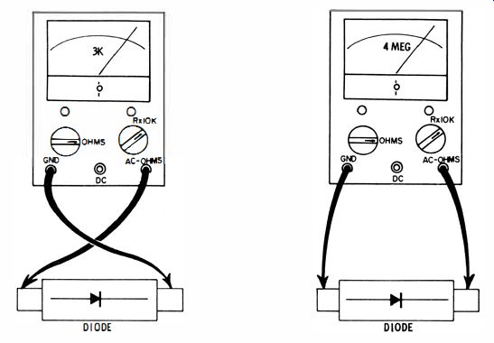
Fig. 12. Checking a semiconductor diode.
Resistance Change Due to Aging
Most resistive components eventually change in value and characteristics as a consequence of aging. In the case of selenium diodes, this is generally recognized as an increase in forward resistance (Fig. 13B), although aging can, and often does, cause a decrease in back resistance. Hence, aging reduces the front-to-back ratio of the diode. The change due to aging is irreversible but resistance changes due to temperature variations are reversible.
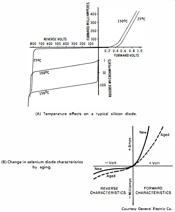
Fig. 13. Change in diode characteristic due to temp. end aging.
(A) Temperature effects on a typical sil icon diode. (b) Change in selenium diode characteristics by aging.
Bilateral and Unilateral Resistances
It is clear that resistive components can be categorized into bilateral and unilateral types. Fig. 14 illustrates this classification. A wirewound resistor can be regarded as a bilateral linear resistance (Fig. 14A), provided it is operated at low temperatures. The term bilateral simply means that the resistance remains the same when the applied voltage is reversed in polarity. The resistance is linear because the current flow is proportional to applied voltage.
Next, observe the bi lateral nonlinear resistance characteristic shown in Fig. 14B. At any applied voltage the current flow remains the same when the polarity is reversed. Hence, this indicates a bilateral resistance. However, the current flow is not proportional to the voltage. Accordingly, it is termed a bilateral, nonlinear resistance. A thermistor or a lamp filament is in this class. Recall that the characteristic of a filament curves downward, whereas the characteristic of a thermistor curves upward ; these curvatures are differences of detail and do not change the general classification of the component.
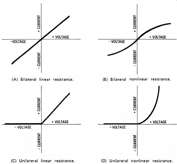
Fig. 14. Characteristic curves of bilateral and unilateral resistances.
(A) Bilateral linear resistance. (B) Bilateral nonlinear resistance. (C) Unilateral linear resistance. (D) Unilateral nonlinear resistance.
Note the unilateral, linear resistance characteristic depicted in Fig. 14C. It is unilateral because current flows only for one polarity of applied voltage. When the voltage is reversed in polarity, no current flows. In the conduction interval, the current is proportional to the voltage. Accordingly, the characteristic depicts unilateral, linear resistance. An ideal diode would have this characteristic. However, in the present state of the art, ideal diodes can only be approximated in practice.
Finally, observe the unilateral, nonlinear resistance characteristic shown in Fig. 14D. As before, this is a unilateral resistance because current flows for only one polarity of applied voltage. Inasmuch as current flow is not proportional to voltage over the conduction interval, the unilateral resistance is a nonlinear resistance. This characteristic approximates diode resistance more closely than the previous classification.
Nevertheless, still other factors must be considered to characterize a diode with maximum accuracy.
Reverse Current
From Fig. 13, it is evident that a semiconductor diode is not strictly a unilateral, nonlinear resistance because a small, reverse current flows-the reverse current is not quite zero.
Strict classification therefore requires that a semiconductor diode be termed an unsymmetrical, nonlinear resistance. The diode actually conducts for both polarities of applied voltage, but the reverse conduction is very small in comparison with forward conduction.
Beginners sometimes suppose that the reverse current is always very small, and might be neglected in practice. However, the reverse current is often put to practical use in electronic equipment. Fig. 13A shows that when the reverse voltage is increased to a certain critical value (800 volts in this example ), the reverse current starts to increase with extreme rapidity. The reverse current now increases much faster than the forward current. If there is insufficient series resistance in the external circuit, the diode will be destroyed by reverse current flow.
Zener Resistance
The reverse-current interval past 800 volts in Fig. 13 is called the zener resistance region. This is a very low positive resistance. The 800-volt point on the reverse characteristic is called the zener point. All diodes do not have an 800-volt zener point. Fig. 15 shows three commercial zeners (HB-1, HB-2, and HB-3 ) that have comparatively low critical voltages.
The zener point depends chiefly on how much doping concentration is used in the semiconductor materials.
Zener diodes are commonly used as clippers, voltage regulators, electronic switches, and for meter protection. In each of these applications, the zener point is of interest and may need to be measured. All diodes have manufacturing tolerances which are quite wide in some cases. A clipping application can require matched diodes that have practically the same zener voltage. Again, a zener diode that is used for meter protection must "break down" slightly past the full-scale indication.
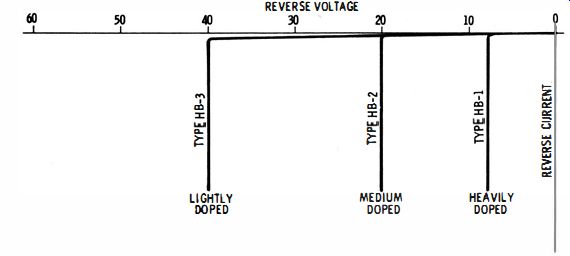
Fig. 15. The zener voltage point depends on the doping concentration used
in the semiconductor materials.
Testing Zener Diodes
A test setup for checking the zener voltage point as well as zener resistance is depicted in Fig. 16. The power supply must provide sufficient voltage to reach the zener point. For example, if the zener diode is rated for 8 volts, a bench power supply with 10 or 12 volts output is suitable. Be sure to set the 5K potentiometer to minimum before connecting the zener diode in the circuit. Also, check to see that you are connecting the diode so that reverse voltage is applied.
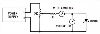
Fig. 16. Test setup for zener diode.
Now, advance the potentiometer in small steps. The voltage across the diode may be increased at first in 2-volt steps, unless it has a very low voltage rating. Note the small current increase at each step. Caution: Reduce the voltage steps as you approach the 1'ated zener voltage. When the milliammeter reading starts to rise rapidly, you are passing through the zener point. The voltmeter reading then checks the actual zener voltage against the rated value.
Next, the zener resistance can be determined to a rough approximation. It is difficult to measure accurately because the Zener resistance is small. Advance the potentiometer very carefully, to avoid damage to the meter and/or the diode. First, pass the zener point and enter the zener region. You might start with a current of 1 ma, for example. Note the voltmeter reading. Then, advance the potentiometer slightly for a current flow of, say, 11 ma. Again, note the voltmeter reading. In this example, the current change is 10 ma.
Suppose the voltmeter reading has changed 0.1 volt. Then, since R = E/I, the zener resistance is 0. 1/0.01, or .10 ohms.
The difficulty in reading 0.1 volt on the 10-volt scale of an ordinary voltmeter illustrates the source of the large experimental error that you can expect.
Power in a Zener Diode
The power dissipated by a zener diode or other type of diode is calculated in the same manner as for an ordinary resistance.
In other words, power is equal to voltage times current. If you apply 10 volts across the diode, and the current flow is 10 ma, the diode dissipates 0.1 watt. The power rating must not be exceeded in any test or application. A very small diode might be rated for a maximum power dissipation of 0.25 watt. A large diode could be rated for 10 watts of dissipation.
OSCILLOSCOPIC METHODS
The simple ohmmeter test depicted in Fig. 12 provides preliminary data, but it is insufficient for many purposes. Incoming inspection, production testing, etc. require that the diode characteristic be checked in detail. Diode characteristics are generally available from semiconductor manufacturers.
These are bogey (average or nominal) characteristics that depict design centers. In other words, manufacturing tolerances cause the actual characteristic of an individual diode to depart more or less from the bogey characteristic. Tolerance limits are often included in diode ratings.
From the previous discussion, it is evident that the voltage versus current values can be measured for a particular diode and the diode characteristic plotted from the meter readings.
Point-by-point meter measurements are tedious and time-consuming. Hence, the automatic curve-tracing method is usually preferred. The oscilloscope test setup depicted in Fig. 17 A continuously displays the complete characteristic on the cathode-ray tube screen. Horizontal deflection is proportional to voltage across the diode, and vertical deflection is proportional to current flow through the diode. Resistor R must be sufficiently great to prevent excessive current flow through the diode.
Voltage and current values can be read directly from the scope screen, if the scope has been previously calibrated.
Calibration is accomplished by applying known voltages in turn to the vertical and horizontal channels of the scope, and adjusting the gain controls for convenient units of deflection.
Current values are measured on the screen with reference to the resistance values across which the vertical-input terminals are connected. A typical diode characteristic is illustrated in Fig. 17B. Note that the display may appear right side up, or upside down, or reversed left-to-right. This simply depends on the deflection polarity of the particular oscilloscope and on the polarity with which the diode is connected into the test circuit.
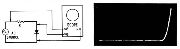
Fig. 17. Checking the voltage-current characteristic of a diode. (A) Oscilloscope
test setup for diodes. (B) Typical voltage current waveform.
The source voltage in Fig. 17 is a sine wave. It makes no difference whether the voltage source is a true or distorted sine wave, sawtooth wave, or other shape ; different wave-shapes will merely vary the brightness distribution in the pattern. A square wave is least desirable in displaying EI curves, because the source voltage then changes very rapidly over the leading and trailing edges ; in turn, the ends of the pattern appear bright, and the characteristic is very dim.
Junction Capacitance
All diodes have junction capacitance, which is usually small enough so that the scope pattern is not noticeably distorted in a 60 -hz test. On the other hand, selenium diodes have a comparatively high junction capacitance which generally introduces distortion at 60 cycles. Some diodes have a very large junction capacitance compared with their back resistance. In such case, pattern distortion (looping) as seen in Fig. 18 makes the test impractical. Either the test frequency must be considerably reduced, or meter readings employed in a point-by-point test.
The looping in Fig. 18 results from the leading current drawn by the junction capacitance. In turn, the voltage drop across R in Fig. 17 A is out of phase with the drop across the diode. If the test frequency is sufficiently low, the reactance of the junction capacitance becomes so high that negligible leading current is drawn. In case a DC test is made with meters, the reactance becomes infinite and introduces no error in determination of the resistance characteristic.
When it is desired to measure junction capacitance in a laboratory or factory, an oscilloscope method is used. The procedure and evaluation of test data are comparatively involved and cannot be covered here. Interested readers are referred to advanced texts for detailed derivations and discussion.
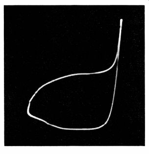
Fig. 18. Severe looping in the pattern.
NEGATIVE RESISTANCE
When the test depicted in Fig. 17 is made with a germanium diode, such as a 1N34A, and the source voltage is sufficient, the reverse interval of the diode characteristic is traced out to the turnover point and into the negative resistance region. A typical pattern is seen in Fig. 19. Note that this pattern happens to be reversed from left to right, compared to the pattern shown in Fig. 17. When displaying negative resistance, be sure to make the series resistance R in Fig. 17 sufficiently large so that the diode is not damaged by the peak current flow.
Consider the pattern in Fig. 19. As the reverse voltage increases, the reverse current also increases and finally starts to rise very rapidly. The end of the reverse characteristic curves, and its maximum excursion at the right-hand end in Fig. 19, is called the turnover point. At this point, the diode resistance is zero. Past the turnover point, the trace begins to curve back again-the voltage is decreasing, but the current is still increasing. This is the definition of negative resistance less voltage causes more current to flow, and vice versa. The external series resistance sets a maximum limit to the current which passes through a maximum at the bottom of the pattern and then returns back to the origin.
Source of Negative Resistance
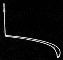
Fig. 1.19. Diode driven into negative· resistance region.
What is the source of the negative-resistance interval past the zero-resistance point in Fig. 19? In a point-contact germanium diode, the development of negative resistance is based on generation and radiation of heat at the contact point. As in all semiconductor diodes, junction resistance decreases with increasing heat. This decreasing resistance is first seen as a downward slope in the reverse characteristic until the zero-resistance point is passed. The slope of the curve is vertical (infinite ) at the turnover point. Then, a negative resistance is entered because the diode can no longer radiate the heat as fast as it is generated by the J2R power factor. Now, a run away condition exists. The junction resistance decreases, and the current increases in an avalanche process.
Although the current is increasing, the voltage drop across the diode is decreasing because the heat build-up is decreasing the junction resistance out of proportion to the voltage. This is evidently an unstable condition, and the diode will be destroyed unless the current is limited by a sufficient amount of external positive resistance. After the current peak is passed, the characteristic reverses its slope (the diode resistance is now positive ), and the retrace follows another path back to the origin. This looping is the result of heat radiation that is now decreasing instead of increasing.
Measurement of Negative Resistance
Negative resistance can be measured from the screen pattern, provided the scope has been previously calibrated. As shown in Fig. 20, a tangent is placed at a selected point on the negative-resistance characteristic. The slope of the tangent gives the value of the negative resistance. Any tangent line so considered defines at its ends a certain voltage interval corresponding to a certain current interval. The quotient of the voltage divided by the current gives the negative-resistance value.
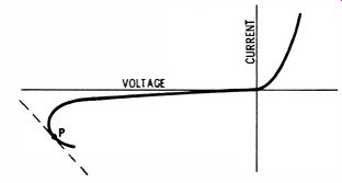
Fig. 20. The negative resistance value curve.
Note that the negative-resistance interval passes through all possible values from zero to minus infinity. The negative resistance is very small just past the turnover point and approaches infinity just before the peak-current point. In suitable circuitry, you can bias the diode to a chosen value of negative resistance and use it as an amplifier or an oscillator. However, the life of a germanium diode is limited in such applications because of the large amount of heat that is generated. Hence, negative-resistance devices commonly use tunnel diodes that can be operated at low temperatures.
TUNNEL DIODES
Unlike a germanium diode, a tunnel diode has a negative resistance interval on its forward-current characteristic. A typical EI curve is depicted in Fig. 21. The negative resistance interval occurs from 55 mv to 350 mv. The value of the negative resistance at a chosen point is given by the slope of the tangent to the curve at that point. It is not as easy to check out a tunnel diode as an ordinary diode. First, unless the external circuit resistance is very low, the tunnel diode operates as an electronic switch, and it is impossible to plot or display the negative-resistance interval. Second, unless the test-circuit reactance is strictly minimized, the system will oscillate even though the circuit resistance is sufficiently low.
Testing Tunnel Diodes
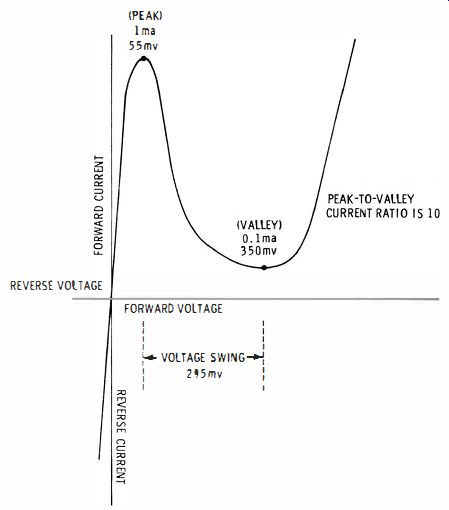
Fig. 21.
Typical tunnel diode voltage current characteristic.
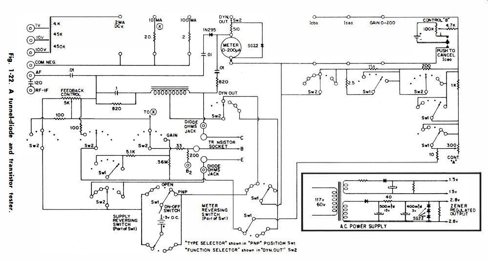
Fig. 22
An ohmmeter will show whether a tunnel diode is open or shorted, but it gives no further information. Hence, service-type testers such as depicted in Fig. 1-22 often provide a switching-circuit test. The tunnel diode is tested for the electronic switching action previously mentioned. This test principle is seen in Fig. 23B. Here is how it works. When the potentiometer is set to minimum, no voltage is applied across the diode, and no current flows. This corresponds to point 1 on the characteristic in Fig. 23A. Next, as the potentiometer is advanced, a load line is established, as shown by the dashed line on the characteristic. Voltage is now applied, and current flows, as indicated by the milliammeter. Further advance of the potentiometer raises the load line to the peak-current point, as shown by the solid line on the characteristic in Fig. 23A. The peak-current flow occurs at point 2 and is indicated by the milliammeter. This is the first part of the test, inasmuch as tunnel diodes are rated for peak-current value.
Now, a slight increase of voltage results in switching action that occurs as follows: The path of operation is not along the negative-resistance interval ; in all configurations of this type, the path of operation is along the load line. Hence, the current flow is not indicated at points 3 and 4, for example. Instead, the meter reading suddenly drops and indicates the current at point 5 in Fig. 23A. Now, if you back off on the potentiometer, the current flow will reduce still further until the load line passes through point 4. This is the minimum or valley current and is the second part of the test, inasmuch as tunnel diodes are rated for valley current.
CURRENT
(A) Voltage current characteristic. (B) Switching circuit test setup.
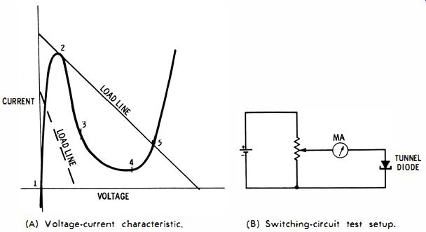
Fig. 23. Switching test for a tunnel diode.
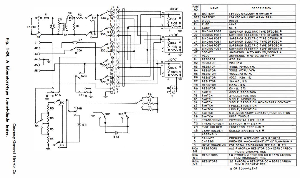
Fig. 24
To summarize, this type of tester checks tunnel diodes by measuring the peak and valley current values. It gives no detailed information concerning the negative-resistance interval because it provides electronic-switching action only. More elaborate types of testers are used by laboratories and factories. These are critically designed using the basic principle shown in Fig. 17 to trace out the complete diode characteristic while avoiding switching action and/or oscillation. This requires a low-resistance series sweep circuit and low inductance test leads.
Lab-Type Tester
A lab-type, tunnel-diode tester is diagrammed in Fig. 24. Jig A is used to test 1- and 2.2-ma diodes. Jig B is for 4.7- and 10-ma diodes. Jig C is for 22-ma units. Vertical and horizontal scope inputs are taken from the V and H points in the jig that is in use. The AC output from T2 then sweeps out the characteristic on the scope screen. Details of control settings for various diodes are not covered here, but interested readers may refer to advanced texts such as the Tunnel Diode Manual published by the General Electric Co.
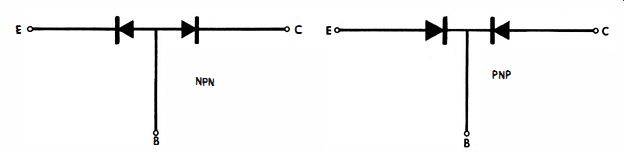
Fig. 25. Equivalent circuits for transistors.
TRANSISTORS
Some transistor tests are essentially the same as diode tests. For example, ohmmeter tests can be made to weed out definitely defective transistors. Preliminary equivalent circuits for transistors can be considered in such tests as are depicted in Fig. 25. The transistor is regarded as two diodes connected back-to-back. Although only a rough approximation, an equivalent circuit of this sort is a guide in making simple resistance tests.
For example, a reasonably high front-to-back ratio is anticipated between emitter and base terminals, as well as between collector and base terminals. If forward current flow (low resistance ) is found when the negative ohmmeter lead is connected to the emitter and the positive lead to the base, the transistor is identified as an NPN type. The opposite finding indicates a PNP type.
You might or might not measure a substantial front-to-back ratio from emitter to collector, even if the transistor is in good condition. A few transistors are symmetrical, meaning that the emitter and collector junctions have identical characteristics.
In this case, the front-to-back ratio from emitter to collector is unity. On the other hand, most transistors are unsymmetrical, which means that you will measure a definite front-to-back ratio from emitter to collector although this ratio is usually lower than the other two ratios. Ohmmeter measurements on a "good" transistor selected at random are noted in Fig. 26.
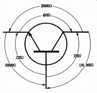
Fig. 26. Ohmmeter test for forward and reverse junction resistances.
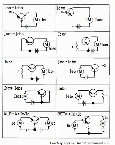
Fig. 27. Basic transistor test circuits.
Junction Resistances
Simple transistor testers, which may have certain supplementary tests, are basically ohmmeters. A common follow-up test is measurement of Junction back resistances in terms of current flow. Nearly all testers provide for a test of I_eo (also called I_cbo) , which is a measurement of leakage current. An I_co test applies a moderate reverse voltage between collector and base with the emitter open, as seen in Fig. 27. A microammeter in the collector circuit indicates whether the back resistance of the collector junction is acceptably high. Transistor manufacturers rate their various types for 1"0 values.
An I_ces (also called I_ebs ) test is made in the same manner as an I_co test, except that the emitter is shorted to the base, as depicted in Fig. 27. The I_bs current flow is normally somewhat greater than the 1"0 current flow. Transistors are customarily rated for I_es as well as I_co. Simple transistor testers seldom provide an lees function.
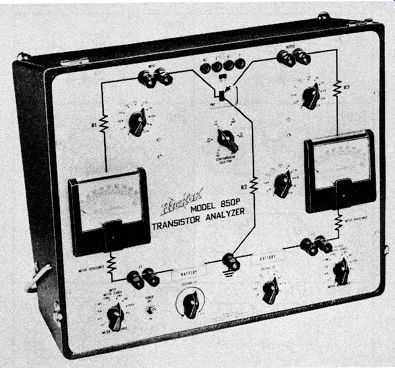
Fig. 28. A transistor tester providing wide choice of test configurations.
The Ieh, test shown in Fig. 27 is intermediate to the I_co and I_ tests. A resistance (commonly 10K) is connected between emitter and base during measurement of reverse collector current. The meter will normally indicate a value greater than I_, but less than I_ces' The more elaborate types of transistor testers provide for measurement of both I_co. and I_cb,. Observe that an I.,," (also called Ie',, ) test is basically the same as an I_co. test, except that emitter and collector terminals are reversed. That is, the reverse emitter-junction current is measured with collector shorted to base. In a truly symmetrical transistor, the I_co and I_es readings are normally the same. Of course, most transistors are unsymmetrical, and the Ices rating is different from the I_c, rating.
Many transistor testers provide an I_co test, as shown in Fig. 27. An I_co reading is normally greater than an I_co reading because the reverse current is increased by emitter-base junction action. This test, as well as the foregoing tests, are provided by instruments which feature maximum flexibility for DC tests (Fig. 28).
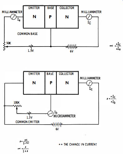
Fig. 29. Alpha and beta relationships.
Observe that an I_co test compares with an I_cbr test in the way that an I_co measurement compares with an I_co measurement. The base-emitter resistor has a typical value of 10K. As would be anticipated, an I_cer reading is normally higher than an I_cbr reading.
The I_co (also called I_co) and I.b, tests depicted in Fig. 27 are emitter-junction tests which are the counterpart of the I_co and I_cb, collector-junction tests. The resistor used in the I_co, test has a value of approximately 10K. Note that the test voltage employed in each of the foregoing tests is not critical-a comparatively low voltage will provide a test point on the flat portion of the reverse-resistance characteristic. Of course, an excessively high test voltage must not be used, because the transistor will be irreparably damaged if the rated voltage is exceeded.
Measurement of Alpha and Beta
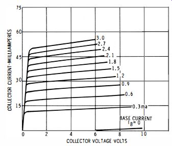
Fig. 30. Example of alpha crowding.
A more critical test of a transistor is made by measuring its alpha or beta. Basically, this is the measurement of transfer resistance. As shown in Fig. 1-27, the emitter is forward biased, and the collector is reverse-biased. A forward emitter bias lowers the emitter junction resistance, which is transferred by lattice action as a lowering of the collector junction resistance. Alpha is defined as the ratio of emitter-to-collector current. Beta is defined as the ratio of base-to-collector current.
The simple ratio of input to output currents gives the DC alpha or beta of a transistor. This is a test that simulates large-signal operation of a transistor, in which the input signal drives the transistor over a large excursion of its characteristics. On the other hand, transistors are commonly rated for small-signal operation, and published values of alpha and beta must be checked by a slightly elaborated procedure.
Incremental Test
To check small-signal alpha and beta, the input current is set to an operating value specified by the transistor manufacturer. This establishes an operating point at a median in the characteristics, as would be used for Class-A amplification.
Then, the input current is increased by a small amount. The corresponding change in collector current is noted. The small signal alpha or beta is then given by the ratio of input-current change to output-current change. Alpha and beta are simply related to each other, as shown in Fig. 29.
The DC alpha or beta will have a different value from the small-signal alpha or beta because the transfer resistance of many transistors is non-linear as seen in Fig. 30. Note that a base-current change from 0 to 0.3 ma produces a much larger collector-current change than a base-current change from 0.9 to 1.2 ma. Hence, this transistor will measure a larger DC beta than its small-signal beta.