AMAZON multi-meters discounts AMAZON oscilloscope discounts
Before getting into transistor theory, there are a few definitions that are better discussed in advance.
Preliminary Definitions
Gain is a term used to describe a ratio of increase. The most common types of gain are current gain, voltage gain, and power gain. Gain is simply the ratio of the input (voltage, current, or power) to the output (voltage, current, or power). For example, if a 1-volt signal is applied to the input of a circuit and, on the output, the signal amplitude has been increased to 10 volts, you say that this circuit has a voltage gain of 10 (10 divided by 1 = 10). It is possible to have a gain of less than 1. For example, if the output of a circuit is only one-half of the value of the input, it can be said this circuit has a gain of 0.5. However, it is preferable to say that the output is being attenuated (reduced) by a factor of 2.
The symbol for gain as used in equations and formulas is A. Typically, the uppercase A (symbolizing gain) will be followed by a lower case suffix letter designating the gain type. For example, Ae symbolizes "voltage gain."
Power gain is a specific type of gain indicating that more energy is being delivered at the output (of a device or circuit) than is fed into the input. A transformer, for instance, is capable of providing voltage gain, if it is a step-up transformer; but the secondary current is reduced by the same factor (turns ratio) as the voltage is increased. Because power is equal to voltage times current, the equation seems to balance-equal power in and power out-but this is still not a gain. Additionally, all components have losses. The transformer's efficiency loss is called its efficiency ratio. A good unit will have about a 90% ratio, and the primary to secondary power transfer ratio will always be less than 1.
Therefore, a transformer is not capable of producing power gain. Electronic components capable of providing power gain are called active devices. These include transistors, vacuum tubes, some integrated circuits, and many other devices. Electronic components that cannot produce power gain are called passive devices. Some examples of passive components are resistors, capacitors, transformers, and diodes.
Introduction to Transistors
The development of the transistor was the foundational basis for all modern solid-state electronics. William Shockley, John Bardeen, and Walter Brattian discovered transistor action while working at the Bell Telephone Laboratory in 1947. The term transistor started out as a combination of the phrase "transferring current across a resistor." The important developmental aspect of the transistor is that it became the first "active" solid-state device and opened a new perspective of design ideology. It's hard to imagine what our lives would be like today with out it! A transistor is a solid-state, three-layer semiconductor device. FIG. 1 shows the basic construction of a transistor, and compares transistor construction to diode construction. Note that a diode contains only one junction, whereas a transistor contains two junctions. Because a transistor contains two junctions, it is often referred to as a (dual-junction) bipolar device. FIG. 1 also illustrates how bipolar transistors can be constructed in either of two configurations: NPN or PNP.
Bipolar transistors have three connection points, or leads. These are called the emitter, the base, and the collector. The symbols for bipolar transistors are shown in Fig. 1. The only difference between the NPN and PNP symbols is the direction of the arrow in the emitter lead.
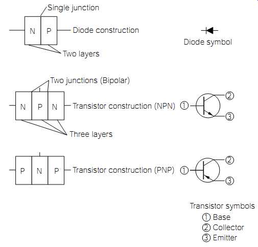
FIG. 1 Transistor construction and symbols.
Transistor Principles
FIG. 2 shows an NPN transistor connected in a simple circuit to illustrate basic transistor operation. A PNP transistor would operate in exactly the same manner, only the voltage polarities would have to be changed. Note that the emitter lead is connected to circuit common (the most negative potential in the circuit) through the emitter resistor (Re ), the base lead is connected to a potentiometer (P1), and the collector lead is connected to 30 volts, through the collector resistor (Rc ).
A transistor actually consists of two diode junctions: the base-to-emitter junction and the base-to-collector junction. Assume that P1 is adjusted to provide 1.7 volts to the base (note how P1 could provide any voltage to the base from 0 to 30 volts). The 1.7-volt potential applied to the P-material base, in reference to the N-material emitter at 0 volts (circuit common), creates a forward-biased diode and causes current to flow from emitter to base. However, because of a phenomenon known as transistor action, an additional current will also flow from emitter to collector.
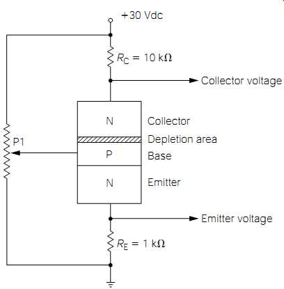
FIG. 2 Simple circuit to illustrate basic transistor operation.
To understand transistor action, we have to consider several conditions occurring simultaneously within the transistor. First, notice that the base-to-collector junction is reverse-biased. The collector is at a much higher positive potential than the base, causing the base to be negative in respect to the collector. Therefore, current will not flow from base to collector. The high positive potential on the collector has the tendency to attract all of the negative-charge carriers (electrons) away from the base collector junction area. This creates a depletion area of negative charge carriers close to the base layer. The depletion area seems very positive for two reasons: (1) all of the negative-charge carriers have been drawn up close to the collector terminal and (2) because it is part of the collector layer, it is connected to the highest positive potential. Keeping this condition in mind, turn your attention back to the base-emitter junction.
Referring again to Fig. 2, as stated previously, the base-emitter junction is forward biased and current is flowing. However, note how the base layer is much thinner than the emitter layer. The emitter has many more negative-charge carriers (electrons) than the thin base material has holes (absence of electrons) to combine with. This causes an "overcrowded" condition of electrons in the base layer. These crowded electrons have two directions in which to flow (or combine, which gives the appearance of flowing); some will continue to flow out to the 1.7-volt base terminal, but the majority will flow toward the very positive-looking depletion area created in the collector area close to the base layer.
The end result is a much higher current flow through the collector than is flowing through the base. The parameter (component specification) that defines the ratio of the base current to the collector current is called beta (abbreviated B or HFE ). In essence, beta is the maximum possible current gain that can be produced in a given transistor. Typical beta values for small-signal transistors are in the range of 100 to 200. In contrast, power transistors can have beta (ß) values of 20 to 70. The equation for calculating beta is:
ß _
Ic
_ I b
This equation states that beta is equal to the collector current divided by the base current. The important point to recognize about transistor current gain is that the higher collector current is controlled by the much smaller base current.
Going back to Fig. 2, assume that the transistor illustrated has a beta of 100. With 1.7 volts applied to the base, about 0.7 volt will be dropped across the base-to-emitter junction (like any other forward-biased silicon diode). The remaining 1 volt (1.7 volts _ 0.7 volt _ 1 volt) will be dropped across the emitter resistor (RE). Because we know the resistance value of RE and the voltage across it, you can use Ohm's law to calculate the current flow through it:
I __ _ 1 milliamp
1 volt
__ 1000 ohms ERE
_ R
The 1 milliamp of current flow through RE is the "sum" of the base current and the collector current. You can think of the emitter as the layer that "emits" the total current flow. The majority of this current is "collected" by the collector, and the overall current flow is controlled by the base. Our assumed beta value tells us that the collector current will be 100 times larger than the base current. Therefore, the base current flow will be about 9.9 microamps, and the collector current will be about 990 microamps (990 microamps _ 9.9 microamps _ 999.9 microamps, or about 1 milliamp). Because the collector current must flow through RC, the voltage drop across the collector resistor (RC) can be calculated using Ohm's law:
E _ IR _ (990 microamps) (10,000 ohms) _ 9.9 volts
There are three individual voltage drops in Fig. 2 that must be analyzed to understand the action of the transistor. Two of these have already been calculated: the voltage across the emitter resistor (RE), and the voltage dropped by the collector resistor (RC).
The third important voltage drop occurs across the transistor itself.
All three of these voltage drops are in series; the emitter resistor is in series with the transistor, which is in series with the collector resistor.
Going back to our discussion of simple series circuits, you know that the sum of these three voltage drops must equal the source voltage of 30 volts. Because you already know the value of two of the voltage drops, you can simply add these two values, subtract the sum from the source voltage, and the difference must be the voltage drop across the transistor:
1 volt (RE) _ 9.9 volts (RC) _ 10.9 volts 30 volts source _ 10.9 volts _ 19.1 volts
Although 19.1 volts are being dropped across the transistor, this is not the collector voltage. Unless otherwise noted, all voltage measurements are always made in reference to circuit common (or ground, whichever is applicable). Therefore, to calculate the collector voltage, the voltage drop across the transistor is added to the voltage drop across the emitter resistor (RE). This must be done because, from a circuit common point of reference, the emitter resistor voltage drop is in series with the transistor voltage drop. If this is confusing, look at it this way. If you made the source voltage your point of reference and measured the collector voltage, you would actually be measuring the voltage drop across RC. If you made the transistor's emitter lead your point of reference, and measured the collector voltage, you would be measuring the voltage across the transistor. By making the circuit common your point of reference, you are actually measuring the voltage across the transistor and the voltage drop across RE. Therefore, the collector voltage would be 1 volt (RE) _ 19.1 volts (transistor voltage drop) __20.1 volts Notice that this is the same value you could have calculated by simply subtracting the voltage drop across the collector resistor (RC) from the source voltage. Now, observe transistor action by changing the base potential.
NOTE: To eliminate redundancy, many of the previous calculations and discussions will not be repeated.
Assume that P1 is adjusted to increase the base bias potential to 2.7 volts.
The base-emitter junction will still drop about 0.7 volts, so the voltage across RE will increase to 2 volts. The emitter current increases to 2 milliamps. With a beta of 100, about 19.8 microamps of the emitter current will flow through the base lead. The remaining 1.98 milliamps of collector current will flow through the collector lead, dropping about 19.8 volts across RC. Subtracting the voltage drop across RC from the 30-volt source produces a collector voltage of 10.2 volts.
When the base voltage was originally set to 1.7 volts, the collector voltage was 20.1 volts. By increasing the base voltage by 1 volt (up to 2.7 volts), the collector voltage decreased to 10.2 volts. In other words, the 1-volt change in the base voltage resulted in a 9.9-volt change in the collector voltage (20.1 volts _ 10.2 volts _ 9.9 volts). This is an example of voltage gain. In this circuit, we have a voltage gain (abbreviated Ae ) of 9.9 (9.9-volt change at the collector divided by the 1-volt change at the base _ 9.9).
There was also an "internal" current gain equal to beta. Obviously, this results in power gain, because both the voltage and the current increased.
If you applied a 1-volt peak-to-peak signal to the base lead of this circuit (Fig. 2), it would be increased to a 9.9-volt peak-to-peak signal at the collector lead. However, the amplified output would be inverted, or 180 degrees out of phase, with the input signal. As you might have noticed, as the base voltage increased (from 1.7 to 2.7 volts), the collector voltage dropped (from 20.1 to 10.2 volts).
There are three "general" transistor configuration methods: the common base, the common emitter, and the common collector. In the previous discussion, involving Fig. 2, you looked at the operation of a common emitter configuration. In this configuration, the output is taken off of the transistor collector, and the signal is always inverted.
If you haven't had any prior experience with transistors, your head is probably "buzzing" with all of the voltages and currents relating to Fig. 2.
Fear not. As you progress and gain experience, the haze will clear, and these principles will seem simple. This section is necessary to provide you with a good working knowledge of basic transistor operational principles.
Now, for practical purposes, you can simplify things according to the transistor configuration. However, before proceeding, there is a very important principle to establish. A bipolar transistor is a "current" device.
Although there will always be voltages present in an operating circuit, the "effect" produced by a transistor is current gain, and the controlling "factor" of a transistor is the input current.
Consider a transistor as being similar to a water valve. A water valve controls the flow of water. Obviously, water pressure must exist to push the water through any type of system, but we never think of a water valve in terms of controlling water pressure (even though pressure changes will occur with differing valve adjustments). A water valve is always used as a device to control the flow of water. Similarly, always think of a bipolar transistor as a device used to control electric current flow.
Common Transistor Configurations
Transistors are "active" devices because they are capable of producing power gain. In actuality, bipolar transistors are current amplifiers, but an increase of current while maintaining the same voltage is an increase of power (P = IE). Depending on the circuit configuration a transistor is designed into, the output can produce current gain, voltage gain, or both. The following transistor circuit configurations will differ in their ability to provide voltage, current, and power gain, but to avoid confusion, a parallel analysis will be given at the end of this section.
Adding Some New Concepts
Before getting into more circuit analysis, it is helpful to understand a few new terms and concepts that will make the whole process simpler.
The remainder of this text contains a lot of discussion involving impedance. While examining some of the basic operational fundamentals of inductors and capacitors, you learned they have a certain frequency dependent nature (this will be discussed further in Section 15). We call such components "reactive." In a reactive component, the opposition to AC current flow is frequency dependent, and these components exhibit a special form of AC resistance called reactance. For example, with inductors, as the frequency of an applied voltage rises, the inductor's opposition to that voltage increases. Capacitive action is just the opposite. In other words, a DC voltage applied to a reactive circuit will promote a current flow dependent on the resistance in the circuit, but an applied AC voltage of the same amplitude might cause a totally different current flow, depending on its frequency. For this reason, you need a term to describe the "total" opposition to AC current flow; taking both the resistive and reactive components into consideration. This term is impedance. Impedance is defined in ohms, just as resistance; it is composed of DC resistance, plus the inductive reactance and/or the capacitive reactance in a circuit; and its symbol, as used in equations and formulas, is Z.
In practical transistor circuits, capacitors are used extensively for a variety of purposes. The following transistor circuits use capacitors for "coupling" (sometimes referred to as "blocking") and "by-pass" functions.
Remember back to our discussions on basic capacitor operation; you know that current cannot pass through the dielectric (insulating) material under normal operation. However, the "effect" of a changing electro static field on one plate can be transferred to the other plate, even though no actual current is passing through the dielectric. Technically speaking, the subatomic distortion occurring on one plate, and in the dielectric, must cause a subsequent distortion in the other plate.
In effect, a capacitor can appear to pass an AC current with virtually no opposition, while totally "blocking" any DC current. A capacitor used to block DC while passing an AC signal current is called a coupling capacitor. There are some situations where we want just the opposite to occur: the DC voltage present with no AC component in it.
Capacitors used for this function are called bypass capacitors. (The previous section covered filter capacitors. Filter capacitors are actually a type of bypass capacitor; they maintain the DC voltage, while reducing the AC component, or ripple.)
In the following transistor configuration circuits, it would be advantageous for you to start thinking of them as "building blocks" to more complex circuits. The most sophisticated electronic equipment can be broken down into simpler subassemblies, and, in turn, these subassemblies can be broken down into basic circuit blocks. In performing electronic design, we start with basic blocks and put them together in such a way that they will collectively produce a desired result. Electronic equipment manufacturers will often include "block diagrams" as part of the overall documentation package for their products. This provides an efficient method of becoming thoroughly familiar with the technical operation of the products, without having to analyze the operation down to a component level. As you gain more experience in the electrical and electronics fields, you'll appreciate the usefulness of a block approach in design, analysis, or troubleshooting ventures.
The Common-Emitter Configuration
As stated previously, you analyzed the circuit in Fig. 2 as though it were a common-emitter amplifier for the purpose of demonstrating voltage gain. In actuality, Fig. 2 can be either a common-emitter amplifier or a common-collector amplifier depending on whether you use the output from the collector or the emitter, respectively. However, a practical common-emitter transistor amplifier would probably require some improvements, as illustrated in Fig. 3.
Bipolar transistors have a negative temperature coefficient; that is, as a transistor's temperature increases, its internal resistances decrease. Also, temperature increases cause an increase in undesirable "leakage" currents that can further add to temperature buildup. In high-power transistor circuits, this chain-reaction temperature effect can lead to a condition called thermal runaway, which renders the circuit inoperative. In small signal transistor circuits, as we are presently examining, varying temperatures will cause shifts in operating points.
In addition to temperature considerations, typical bipolar transistors do not have precise beta values. Manufacturers specify beta values with in minimum and maximum ranges for each transistor type. Consequently, two transistors with the same exact part number can have dramatically differing beta values.
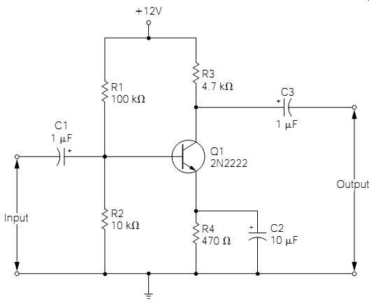
FIG. 3 Practical example of a common-emitter transistor amplifier.
A third problematic variable to consider is the source voltage. Transistor circuits intended to be powered from a battery power supply must be capable of operating with a relatively broad range of supply variance.
Even 120-volt AC line-powered transistor circuits might experience voltage variations if the power supply is not well regulated. A "perfect" transistor amplifier circuit would be self-correcting with temperature variations, unaffected by the transistor's beta value, and totally immune to source voltage variations. Although you can't achieve perfection, you can come close to it with the circuit in Fig. 3.
Notice that P1 (Fig. 2) has been replaced with two fixed resistors to set the base bias. C1 is a coupling (or blocking) capacitor to keep the DC base bias voltage from being applied to the input source. Similarly, C3 serves the same function of keeping the DC collector voltage from being applied to the output. C2 is a bypass capacitor which effectively "shorts" the AC emitter (input signal) voltage to circuit common, while leaving the DC emitter voltage unaffected.
The bias voltage divider, consisting of R1 and R2, keeps the correct percentage of source voltage applied as a base bias, regardless of the actual value of the source voltage. In other words, the actual resistor values in Fig. 3 have been chosen so that about 9% of the source voltage will be dropped across R2 (without considering the parallel base impedance).
Regardless of the actual value of the source voltage, about 9% of it will be applied as a base bias. This has the effect of keeping the bias voltage optimized, even with wide variations in source voltage. Temperature stability is also improved by this method. However, R2 is not absolutely necessary, and it has the undesirable effect (for most applications) of lowering the input impedance. For these reasons, R2 is not incorporated into all common-emitter designs.
Although R4 is commonly called the emitter resistor, from an operational perspective, R4 is also a negative-feedback resistor. Negative feedback is the term given for applying a percentage of an amplifier's output back into the input. This improves amplifier stability, but it also reduces gain.
In Fig. 3, the negative feedback provided by the voltage developed across R4 makes the circuit less dependent on the individual transistor current gain (beta), and aids in increasing temperature stability.
As stated earlier, C2 "couples" (short-circuits) the AC signal to circuit common, but it has little effect on the DC emitter voltage. In reality, this causes two individual gain responses within the circuit. From a DC perspective, C2 doesn't exist. The negative feedback produced by R4 causes the DC voltage gain to be a ratio of the value of the collector resistor (R3), divided by the value of the emitter resistor (R4). With the circuit illustrated, the DC voltage gain is approximately 10. From an AC perspective, R4 doesn't exist, because C2 looks like a short tying the transistor emitter directly to circuit common. Consequently, the AC voltage gain becomes the ratio of the collector resistor value divided by the internal base-emitter junction resistance. The junction resistance of a forward-biased semiconductor junction is very low, so the AC voltage gain is reasonably high, typically in the range of 200, using the 2N2222 transistor as illustrated. This high gain is advantageous, but is highly dependent on individual transistor characteristics. If C2 were removed from the circuit, the AC voltage gain would become the same as the DC voltage gain, or about 10.
The DC input impedance of this circuit (Fig. 3) can be considered infinite, because C1 blocks any DC current flow. The AC input impedance consists of three parallel resistive elements: R1, R2, and the forward biased base-emitter junction resistance multiplied by beta. The forward-biased junction resistance is a low value, typically only a few ohms. Even after multiplying this value by a high beta value, the product would still be much lower than a typical R2 value. Therefore, for practical analysis purposes, you can usually eliminate R1 and R2 from consideration and estimate the input impedance to be the base-emitter junction resistance times the beta value. If C2 is removed from the circuit, the AC input impedance then becomes the parallel resistance value of R1, R2, and the value of R4 multiplied by the beta value. Because R4 times beta is typically a high-resistance value, and R1 is usually a high-resistance value, a reasonably close estimate of the input impedance with C2 removed is the value of R2. The output impedance of this circuit can be considered to be equal to the value of the collector resistor (R3).
FIG. 3 is a good, stable design with reasonably high voltage gain and wide-range immunity from beta, temperature, and source voltage variations. You might use this circuit as a good building block for most voltage amplification applications, or you can tailor the component values according to specific needs.
The Common-Collector Configuration
FIG. 4 is a practical example of a common-collector transistor amplifier. Note that the output is taken off of the emitter instead of the collector (as in the common-emitter configuration). A common-collector amplifier is not capable of voltage gain. In fact, there is a very slight loss of voltage amplitude between input and output. However, for all practical purposes, we can consider the voltage gain at unity. Common-collector amplifiers are noninverting, meaning the output signal is in phase with the input signal. Essentially, the output signal is an exact duplicate of the input signal. For this reason, common-collector amplifiers are often called emitter-follower amplifiers, because the emitter voltage follows the base voltage.
Common-collector amplifiers are current amplifiers. The current gain for the circuit illustrated in Fig. 4 is the parallel resistance value of R1 and R2, divided by the resistance value of R3. R1 and R2 are both 20 K-ohms in value, so their parallel resistance value is 10 K-ohms. This 10 K-ohms divided by 1 Kohm (the value of R3) gives us a current gain of 10 for this circuit. Because the voltage gain is considered to be unity (1), the power gain for a common-collector amplifier is considered equal to the current gain (10, in this particular case).
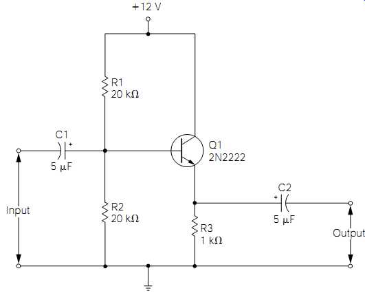
FIG. 4 Practical example of a common-collector (emitter-follower) transistor
amplifier.
The input impedance of common-collector amplifiers is typically higher than the other transistor configurations. It is the parallel resistive effect of R1, R2, and the product of the value of R3 times the beta value.
Because beta times the R3 value is usually much higher than that of R1 or R2, you can closely estimate the input impedance by simply considering it to be the parallel resistance of R1 and R2. In this case, the input impedance would be about 10 K-ohms. The traditional method of calculating the output impedance of common-collector amplifiers is to divide the value of R3 by the transistor's beta value. Although this method is still appropriate, a closer estimate can probably be obtained by considering the output impedance of most transistors to be about 80 ohms. This 80-ohm output impedance should be viewed as being in parallel with R3, giving us a calculated output impedance of about 74 ohms (80 ohms in parallel with 1000 ohms).
Resistors R1 and R2 have the same function within a common-collector amplifier as previously discussed with common-emitter amplifiers. The high negative feedback produced by R3 provides excellent temperature stability and immunity from transistor variables. As in the case of Fig. 3, the circuit illustrated in Fig. 4 can be a valuable building block toward future projects.
The Common-Base Configuration
I have included the common-base transistor amplifier configuration in this text for the sake of completeness, but the applications for it are few.
They are often used as the first RF amplifier stage, amplifying signals from radio antennas, but are seldom seen otherwise.
FIG. 5 illustrates a practical example of a common-base amplifier.
Common-base amplifiers have the unique characteristic of a variable input impedance dependent on the emitter current flow. The equation for calculating the input impedance is
Zin _ 26
_ I e
where I e is the emitter current in milliamps.
As can be seen from the previous equation, the input impedance is low. Furthermore, common-base amplifiers have a high output impedance, and a power gain slightly higher than common-emitter amplifiers.
Transistor Amplifier Comparisons
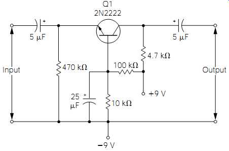
FIG. 5 Practical example of a common base transistor amplifier.
The common-emitter configuration is used in applications requiring reasonably high voltage and power gains. The output is inverted. Common-emitter amplifiers have low input impedances, and high output impedances.
The common-collector configuration is used for impedance-matching applications. Common-collector amplifiers have high input impedances with low output impedances. Voltage gain is considered at unity, and the output is non-inverted.
The common-base configuration is seldom used because of its very low input impedance and high output impedance. Common-base amplifiers also have a very unstable nature at high gain values.
Impedance Matching
FIG. 6 illustrates the importance of correctly matching input and output impedances between circuit stages. The AC signal source illustrated in the left half of Fig. 6 could be the output of a common emitter amplifier, a laboratory signal generator output, the "line" output of a FM radio receiver, or thousands of other possible sources.
The important point is that all signal sources will have an internal impedance; shown as Zs in the illustration. Internal source impedances can range from fractions of an ohm to millions of ohms in value. In this example, assume the internal impedance to be 1000 ohms. The signal level you want to apply to RL is 10 volts peak to peak. Notice that Zs is in series with RL. You know that, in a series circuit, the voltage drop will be proportional to the resistance values.
Therefore, in this circuit, about 9.1 volts P-P will be dropped across the internal source impedance, and only about 0.9 volt P-P will actually be applied to RL. This is undesirable because over 90% of the signal has been lost.
The circuit illustrated in the right half of Fig. 6 shows the same signal source connected to the input of a common-collector amplifier stage.
(Note the triangular symbol for the common-collector amplifier. This is the symbol used for amplifiers in most block diagrams.) Because the amplifier has an input impedance of 10,000 ohms, only 0.9 volt P-P will be dropped across the internal source impedance, and 9.1 volts P-P will be applied to the amplifier. This is much better because the signal loss is only about 9%.
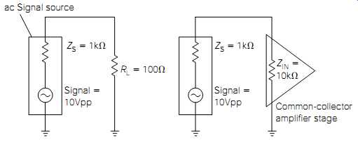
FIG. 6 Demonstration of impedance matching.
Here are a few general rules to remember regarding impedance matching. For the maximum transfer of voltage (as discussed in the previous example), the output impedance should be as low as possible and the input impedance should be as high as possible. For the maximum transfer of power, the output impedance should be the same value as the input impedance. For the maximum transfer of current, the output impedance and input impedance should be as low as possible.
Transistor Workshop
The previous sections on transistor fundamentals can be rather abstract during your first read-through, so if you are somewhat con fused regarding several of the discussions of transistor fundamentals at this point, don't feel bad. The field of electronics is somewhat analogous to finding your way around in a big city for the first time. It's inevitable that you'll get lost occasionally, but with persistence, you soon begin to feel quite at home.
This section is dedicated to illustrating the previous transistor fundamentals in practical circuitry. Although the basic action and physics involved with transistor operation remains the same, the way in which we can utilize these actions is quite varied. In addition, many of the devices and circuits detailed in previous sections will be brought into the context of this transistor workshop. By spending some time studying and understanding the circuit examples in this section, you will be applying the fundamentals of transistor operation in practical ways, and familiarizing yourself with some basic electronic building blocks at the same time! Referring to Fig. 7a, note that a transistor can be thought of, in an equivalent sense, as two back-to-back diodes.
NOTE: You cannot construct a functional transistor from two diodes. The equivalent circuit illustrated is for "visualization" purposes only.
If you have a DVM with a "diode test" function, you can perform a functional test of a typical NPN transistor in the same manner as if it were two common diodes connected together at their anodes. By placing the red (positive) lead of your DVM on the base and the black (negative) lead on the emitter, you should see a low resistance, just like a typical forward-biased diode would provide. Likewise, leaving the red lead connected to the base and placing the black lead on the collector, you should see another low resistance, indicative of another forward-biased semiconductor junction. By reversing the lead orientation (i.e., placing the black lead on the base and the red lead on the emitter or collector), you should read an infinite resistance in both cases. And finally, connecting the DVM leads from emitter to collector, in either orientation, should provide a reading of infinite resistance.
FIG. 7b illustrates the equivalent circuit of a PNP transistor. The same exact principles and physics apply; the only difference is in the polarity of voltages and the corresponding opposite direction of current flow. In the case of PNP transistors, placing the black lead of your DVM (in diode test mode) on the base with the red lead on either the emitter or collector will provide a low resistance, typical of any forward-biased semiconductor junction. Infinite resistance will result from placing the red lead on the base with the black lead connecting to the emitter or collector. And finally, as in the case of "any" bipolar transistor, a resistance measurement from emitter to collector should provide an infinite resistance in either test lead orientation.
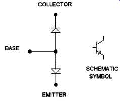
FIG. 7a NPN transistor equivalent circuit and schematic symbol.
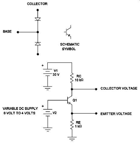
FIG. 7b PNP transistor equivalent circuit and schematic symbol.
FIG. 7c Example circuit to illustrate DC conditions.
It is a good experience-oriented learning task to purchase a grab bag of assorted transistors from any electronics supply house and use your DVM to determine the general type (i.e., either NPN or PNP) and the operational condition (i.e., either "good" or "defective"). Since transistor lead designation is seldom marked on the case, you'll have to make numerous trial-and-error guesses until you can find the base lead and determine the general transistor type. With a little practice, this routine becomes rather second-nature to most electronics hobbyists. It's an inexpensive exercise, and you can always use a variety of transistor types for future experimentation and project building.
Referring to Fig. 7c, note that Q1 is connected to two power supply sources (illustrated as batteries). The V1 source is set at 30 volts DC and is fixed (i.e., it doesn't vary). The V2 source is connected to the base of Q1 and is variable from 0 volts DC to 4 volts DC. We will examine this circuit in several conditions to understand the concept of the current amplification factor, or "beta," of Q1.
Continuing to refer to Fig. 7c, assume the beta parameter for this transistor (Q1) to be 99. As stated previously, beta simply defines the ratio of the base current to the collector current. A beta parameter of 99 means that the collector current will be 99 times higher than the current flowing in the base circuit.
NOTE: Typical transistor beta values can vary from 20 to over 300. I chose 99 for these example problems to make the calculations easier.
If V2 is adjusted for a base voltage of 1 volt, approximately 0.7 volt will be dropped across the forward-biased base-emitter junction, leaving about 0.3 volt to be dropped across the emitter resistor (RE). Since the value of RE is known (1 Kohm) and the voltage across it is known (0.3 volt), the current flow through RE can be easily calculated using Ohm's law:
I __ _ 0.0003 amps or 300 microamps
0.3 volt
__ 1000 ohms E _ R
The current flow through RE is the same variable as the "emitter current flow" of Q1. Therefore, since the total current flow for both base and collector comes from the emitter, you know that the sum of the base current and collector current will equal 300 microamps. In addition, since the beta for Q1 is assumed to be 99, you know that the base current will be 99 times smaller than the collector current. Therefore, the base current will be approximately 3 microamps and the collector current will be approximately 297 microamps (297 microamps divided by 3 microamps _ 99), with both current flows adding up to the total emitter current flow of 300 microamps.
Under the previous conditions, the emitter voltage of Q1 has already been determined to be 0.3 volt (i.e., the voltage across RE). The collector voltage of Q1 will be the V1 source voltage "minus" whatever voltage is dropped by the collector resistor (RC). The voltage drop across RC can be calculated using Ohm's law by multiplying the collector current (297 microamps) by the resistance value of RC (10,000 ohms):
E _ IR _ (0.000297 amps) (10,000 ohms) _ 2.97 volts
Therefore, the collector voltage will be
30 volts _ 2.97 volts _ 27.03 volts
Therefore, with V2 adjusted for 1 volt and an assumed beta of 99 for Q1, the collector voltage will be "about" 27 volts and the emitter voltage will be "about" 0.3 volt. Remember, all specified voltages in a typical schematic will be in reference to circuit common, or ground potential, unless the voltage is accompanied with a specific qualifying statement. Therefore, when measuring the collector voltage of Q1, you are actually measuring the voltage across RE as well as the voltage from emitter to collector of Q1.
Now, assume that all other circuit conditions for Fig. 7c remain the same, with the exception that V2 is adjusted to 2 volts. Subtracting the typical 0.7-volt base-emitter junction drop, the voltage across RE (which is the emitter voltage) will be about 1.3 volts. Using Ohm's law to calculate the emitter current:
I __ _ 0.0013 amp or 1.3 milliamps 1.3 volts
__ 1000 ohms E _ R
Again, assuming the beta of Q1 to be 99, the base current flow will be about 0.013 milliamps and the collector current flow will be about 1.287 milliamps (1.287 milliamps divided by 0.013 milliamp _ 99). The voltage dropped by RC under these conditions will be
E = IR = (1.287 milliamps) (10,000 ohms) = 12.87 volts
Therefore, the collector voltage will be
30 volts - 12.87 volts= 17.13 volts
Therefore, with V2 adjusted for 2 volts and an assumed beta of 99, the collector voltage will be "about" 17 volts and the emitter voltage will be "about" 1.3 volts. As you recall, when V2 was adjusted for 1 volt, the collector voltage was approximately 27 volts and the emitter voltage was approximately 0.3 volt. In other words, an increase of 1 volt to the base of Q1 resulted in a decrease of about 10 volts at the collector (27 volts - 17 volts = 10 volts) and an increase of about 1 volt on the emitter. Imagine that the V2 voltage cycled up and down, like a seesaw, from 1 volt to 2 volts, back to 1 volt, back to 2 volts, and so on. In other words, it is continually changing by 1-volt levels. Under these conditions, the collector voltage of Q1 would be changing by 10-volt levels, but it would be always be going in the opposite direction of the base voltage. If the base voltage increased, the collector voltage would decrease, and vice versa. Therefore, it is said that the collector voltage is 180 degrees out of phase, or inverted, compared to the base voltage. In gist, the collector voltage shows a voltage gain of 10, but it is inverted. In contrast, the emitter voltage is in phase, or non-inverted, compared to the collector, but it exhibits no voltage gain. However, it does provide current gain (i.e., the emitter current is approximately equal to beta times the base current).
You have just examined the fundamental operation of a common emitter amplifier and a common-collector amplifier as discussed in the previous section. Although some variations will occur in these basic circuit configurations to accommodate cost, efficiency, and performance factors, the fundamental difference between a common-collector amplifier and a common-emitter amplifier is simply the decision to use the signal output from either the emitter or collector, respectively. In other words, if you use the signal from the collector, the amplifier is a common-emitter configuration. If you use the signal from the emitter, the amplifier is a common-collector configuration.
Again referring to Fig. 7c, you should be familiar with two more common fundamentals of transistor operation. Suppose that V2 were adjusted to only 0.1 volt. This low base voltage is not sufficient to for ward-bias the base-emitter junction of Q1. Therefore, there is no significant current flow in either the base or emitter. Likewise, since there is no emitter current, there cannot be any consequential collector current.
Without any current flow through RC, the voltage drop across RC is zero. Because the collector voltage of Q1 will equal the V1 voltage (30 volts) minus the voltage drop across RC (zero, in this case), the collector voltage will become the entire V1 voltage, or _30 volts. Likewise, since there isn't any emitter current flow, the voltage drop across RE is zero, and the emitter voltage is therefore zero. A transistor in this condition, where the base current is zero due to insufficient "drive" voltage to pro mote current flow, is said to be cut off, or in a condition of cutoff.
In contrast to cutoff, suppose that V2 in Fig. 7c is increased to 4 volts. Subtracting the normal base-emitter drop of 0.7 volt, this leaves 3.3 volts across RE. Therefore, the emitter current is approximately 3.3 milliamps. Neglecting the small base current and assuming the collector current to be "close" to the emitter current, this would mean that RC would "try" to drop about 33 volts (3.3 milliamps _ 10 Kohm _ 33 volts).
However, this is quite impossible since the V1 power supply is only 30 volts. A transistor circuit in this condition, wherein an increase of the base current (or voltage) causes no further change in collector voltage (or current) is said to be in saturation. As should be readily apparent, cutoff and saturation are the two opposite operational extremes of any functional transistor circuit.
As an aid to visualizing the concepts of cutoff and saturation, assume you adjusted V2 in Fig. 7c down to 0.1 volt and slowly began increasing it. Q1 would remain in cutoff until you reached a V2 voltage of about 0.7 volt. As you continued to slowly increase V2 above 0.7 volt, the transistor circuit would be in its active operational region, because the associated voltages and currents would be changing with the changing base voltage in a linear, or proportional, manner. However, as you continued to increase V2 above 3 volts, you would soon reach a point wherein the transistor circuit would saturate, causing any further V2 increases to have little or no effect on the collector voltage or current.
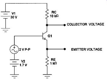
FIG. 7d Example circuit to illustrating AC operation.
The transistor circuit of Fig. 7c is useful for demonstration purposes, but practical amplifiers are called on to amplify AC voltages that periodically change polarities. As illustrated in Fig. 7c, Q1 would fall into its cutoff region whenever an AC signal (applied to Q1's base) started to go into the negative region. For this reason, AC voltages intended to be amplified must be "lifted up" to some DC level that falls within the active operational region of a transistor amplifier circuit to facilitate amplification of the entire AC waveform. Figure 7d illustrates the basic principle of how this is accomplished. Note that Fig. 7d is essentially the same circuit as Fig. 7c with the addition of an AC signal source inserted in series with the V2 DC source of the base lead. The amplitude of this AC signal source is 2 volts peak to peak, which means that it normally rises to 1-volt peaks above the positive level and falls to 1-volt peaks in the negative direction. However, in this case, the AC signal source is in series with a constant DC bias of 1.7 volts. Therefore, as the base "sees" the composite signal, it rises to 2.7-volt peaks in the positive direction (1.7-volt bias _ 1 volt positive peak _ 2.7 volts) and falls to minimum levels of 0.7 volts when the AC voltage reaches its maximum negative-going peak (1.7 volt bias _ 1 volt negative peak _ 0.7 volt). In other words, by causing the AC voltage to "ride" on a steady-state DC voltage, or bias, the base of Q1 never goes below its required 0.7-volt cutoff extreme, and the entire AC signal is amplified by a factor of 10 at the collector of Q1. Therefore, the AC collector voltage signal will be amplified to 20 volts peak to peak, but it will be inverted in respect to the original signal on the base. The emitter voltage will be about 2 volts peak to peak (P-P) (minus a negligible loss of amplitude), but it will be noninverted and the current gain will be approximately equal to beta. (The importance of this current gain factor will become clear in a few circuit examples presented later.) The principle of establishing various steady-state DC levels to place transistorized circuits into their most optimized active operational regions is called biasing. The steady-state DC levels used in establishing a correct bias are typically called the quiescent settings. The term quiescent refers to the "steady-state conditions" of any electronic circuitry, in contrast to the term dynamic, which applies to the "changing conditions" of electronic circuitry.
Although Fig. 7d illustrates the principle of establishing a functional base bias for Q1, Fig. 7e illustrates a more practical method of accomplishing the same thing. Note that a simple voltage divider, consisting of R1 and R2, has replaced the V2 bias source of Fig. 7d.With the resistance values chosen, the positive quiescent voltage applied to the base of Q1 will be about 2.2 volts (2.2 volts is a little more "optimum" than 1.7 volts for pro viding the largest possible collector voltage swings). Since the voltage divider receives its operational power from the 30-volt V1 supply, only one power supply is required for operation. Rather than placing the AC source in series with the bias voltage, coupling capacitor C1 is used to sum the AC voltage onto the quiescent DC base voltage. Remember, a capacitor will appear to easily pass AC voltages while blocking DC voltages. Therefore, the DC voltage on the positive plate of C1 is the 2.2-volt base bias, but the DC voltage on the negative plate will be zero. Thus, the AC signal voltage is superimposed on (i.e., added to) the DC quiescent base bias; the end result is essentially the same as if the AC source were in series with the base bias voltage.
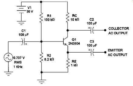
FIG. 7e Example circuit to illustrating a practical method of base bias.
Again referring to Fig. 7e, capacitors C2 and C3 provide the same type of coupling action as C1. The DC quiescent voltages on the collector and emitter of Q1 will be blocked by capacitors C2 and C3, respectively, providing only the "amplified" pure AC signal at the outputs. Note that the AC signal source of Fig. 7e is set to 0.707 volt RMS at a frequency of 1 kHz. Also, 0.707 volt rms is the same level of AC sinewave voltage as 2 volts P-P (0.707 volt rms _ 1 volt peak _ 2 volts P-P. If this is confusing, you should review the basic concepts of AC waveshapes provided in the beginning of Section 3 of this textbook.). The 1-kHz frequency denotes that 1000 complete cycles of AC voltage occur in every 1-second time period.
If you were to construct the Fig. 7e circuit exactly as illustrated, applying an AC signal input at the amplitude and frequency shown, you would obtain an inverted replication of the base signal on the "collector AC output" connection, with the amplitude increased to a level of 7.07 volts rms (a gain factor of 10). In addition, you would obtain an "exact" copy of the base signal at the "emitter AC output" connection (i.e., non inverted), and the amplitude would be almost identical to the base signal (there will be a slight, usually negligible, voltage amplitude "loss").
The amplifier circuit of Fig. 7e is a practical and well-performing single-stage (i.e., only one transistor stage is used) transistor amplifier that can be used in a variety of real-world applications. It will function well using a wide variety of transistor types and power supply voltages. Keep in mind that transistor amplifiers are seldom designed for the purpose of using the outputs from both emitter and collector simultaneously. If voltage gain is desired, the output will be taken exclusively from the collector, which classifies the amplifier circuit as a common-emitter configuration. In contrast, if only current gain is desired, the output will typically be taken from the emitter, which classifies the amplifier circuit as a common collector (or emitter-follower) design. Output coupling capacitors (such as C2 or C3 in Fig. 7e) may or may not be incorporated, depending on whether it is important to remove the "DC" component from the output signal.
As discussed briefly in the previous section, the voltage gain of the Fig. 7e amplifier circuit is established by the ratio of the collector resistor and emitter resistor. The 10-Kohm collector resistor (RC) divided by the 1-Kohm emitter resistor (RE) equals 10; therefore, the voltage gain is 10. If RE were reduced in resistance value, the voltage gain would rise proportionally, and this process would continue until the voltage gain approached the value of beta (HfE ). Since voltage gain is actually a product of the current gain (beta) converted to a voltage drop across the collector resistor, the voltage gain at the collector of Fig. 7e could never go above the beta value of Q1. However, there are practical limits to the gain obtainable in a single-stage amplifier that relate to both repeatability and stability.
Examining the concepts of stability first, suppose you needed a voltage amplifier with a voltage gain of 200, so you reduced the value of RE in Fig. 7e to 50 ohms to cause the RC/RE ratio to equal 200. Provided the beta value of Q1 were well above 200 and the bias voltage to the base were reduced, you could achieve your desired gain, but the circuit would become very unstable. This is because Q1 would be amplifying all changes to the base voltage, both AC and DC, by a factor of 200. As stated previously in this section, transistors, as well as most solid-state components, are sensitive to temperature changes. Typical ambient-temperature changes around Q1 would create small DC bias voltage changes on the base, which would be amplified by a factor of 200, and result in large DC shifts in the quiescent operating points. In other words, the circuit might work at 70 degrees, but become totally inoperative at 80 degrees. Therefore, it is said to be unstable, because its proper operation is easily hampered by normal, anticipated environmental changes.
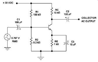
FIG. 7f Example circuit illustrating the effect of adding a bypass capacitor.
The unstable attributes of single-stage transistor amplifiers operating at high voltage gain levels can be corrected by the modifications illustrated in Fig. 7f. Note that RE has been bypassed with a capacitor (C3) and the output signal is taken from Q1's collector. This modification essentially separates the AC and DC gain factors. Since a capacitor blocks any DC current flow, C3 looks like (resembles) an open circuit to the DC quiescent emitter voltage, so the DC gain of the Fig. 7f circuit is simply the RC/RE ratio, which comes out to 10. In contrast, C3 looks like a short circuit to AC voltages, so the AC voltage gain factor increases to the maximum level allowed by Q1's beta. Depending on Q1's beta value, the actual AC voltage gain of this circuit will probably be about 200. This circuit will be very stable as illustrated, because the voltage gain associated with the DC quiescent operational levels is held at 10, but it will not be very repeatable.
Repeatability applies to the capability of being able to reproduce the identical set of operating characteristics within multiple identical circuits. For example, suppose you constructed the circuit of Fig. 7f, compared the input signal to the output signal, and discovered the actual AC voltage gain to be 180. If you then removed Q1 from the circuit and replaced it with another identical 2N3904 transistor, would the AC voltage gain still be 180? In all probability, it would not. Transistors are not manufactured with exact beta values; rather, they are specified as meeting a required range or minimum beta value. Two identical transistors with the same part number could vary by more than 100% in their actual beta values. Since the AC voltage gain of Fig. 7f is largely dependent on the beta value of Q1, you could construct a dozen identical circuit copies of Fig. 7f and achieve variable AC voltage gains ranging from 120 to 250. Therefore, the repeatability of such a circuit is said to be poor.
In its simplest form, you can think of any single-stage transistor amplifier circuit as a "block" with an input and an output. Like all electronic circuits having inputs or outputs, there will always be some finite input impedance and output impedance. So far in this section, you have examined the internal functions of transistor amplifiers, but it is also important to understand the effect such amplifiers have on external devices or circuits.
Referring back to Fig. 7e, the AC signal source in this illustration could represent a wide variety of devices. It could be a lab signal generator, a previous transistor amplifier stage, a signal output from a radio, the electrical "pickup" from an electric guitar, and the list goes on and on. It represents any conceivable AC voltage that you want to amplify for any conceivable reason. Regardless of what this AC signal source represents, it will have an output impedance. In order for transistor amplifiers to function well in a practical manner, the output impedance of the intended signal source must be compatible with the input impedance of the transistor amplifier. Otherwise, your intended amplifier may turn out to be an attenuator (i.e., a signal reducer).
Before going into a detailed description of input and output impedances, it is important to understand that all power supplies look like a low impedance path to circuit common (or ground potential) to AC signals. In other words, the internal impedance of all high-quality power supplies must be very low. As a means of understanding this principle, you can try a little experiment with a common 9-volt transistor battery (the small rectangular type used in low-power consumer products) and a 100-ohm resistor. First, measure the DC voltage at the battery terminals with your DVM. If the battery is new, you should read about 9.4 volts, or a little higher. Now, using a couple of clip leads, connect a 100-ohm, 1/2-watt resistor across the battery terminals and quickly measure the voltage across the resistor (the resistor will become hot if you leave it connected to the battery for more than a few seconds). You should see a noticeable "drop" in the battery output voltage. This "drop" in output voltage represents the voltage dropped across the "internal impedance" of the battery. When I tried this experiment with a new battery, I measured 9.46 volts "unloaded" (i.e., without any load placed on the battery) and 9.07 volts "loaded" (i.e., with the 100-ohm resistor connected across the battery's terminals). You will probably obtain similar results. By performing a simple Ohm's law calculation, you can use your unloaded voltage and loaded voltage measurements to determine the internal impedance of the battery. For example, in our case, the difference between 9.46 volts (unloaded) and 9.07 volts (loaded) is 0.39 volt. This tells me that while 9.07 volts was being dropped across the external 100-ohm resistor, 0.39 volt was being dropped across the internal impedance of the battery. The current flow through the 100-ohm resistor while it was connected to the battery was:
I __ _ 0.0907 amp or 90.7 milliamps 9.07 volts
__ 100 ohms E _ R
Since the battery and 100-ohm resistor were in series with each other while connected, the previous calculation tells me that the internal impedance of the battery was a resistance value that caused 0.39 volt to be dropped when the current flow was 90.7 milliamps. Using these two known variables, I can now calculate the actual internal impedance of the battery:
R __ _ 4.299 ohms
0.39 volt
__ 0.0907 amp E _ I
If you happen to try the same experiment with a used battery, you will discover that the difference between its "unloaded" and "loaded" voltages is much more extreme. In other words, as batteries become drained of their energy-producing capabilities, their internal impedance rises. An ideal power supply would exhibit zero ohms of internal impedance.
Taking the principle of the low impedance characteristic of power supplies one step further, refer back to Fig. 4 of the previous section.
Imagine you were going to use this simple power supply circuit to provide operational power to a transistor amplifier stage, similar to that shown in Figs. 7e or f. The transistor amplifier stage would take the place of Rload as illustrated in Fig. 4 (prev. section), so capacitor C1 would be in parallel with the entire amplifier stage. As stated previously, capacitors look like a short to AC voltages (typically), so from the perspective of any AC signal voltage, the positive side of C1 would appear to be connected directly to circuit common. Therefore, AC line-operated DC power supplies also appear to have extremely low internal impedances from the perspective of any AC signal voltages.
Keeping the aforementioned principles in mind, refer to Fig. 7e once again. Note that the top end of R1 connects directly to the 30-volt power supply. However, from the perspective of the AC signal source, the top end of R1 connects directly to circuit common, because the internal impedance of the power supply is assumed to be very low.
FIG. 7g is an equivalent circuit used to illustrate the AC input impedance of the transistor amplifier circuit of Fig. 7e, where Zs symbolizes the output impedance of the AC signal source. Although C1 is shown, note that it is shorted from the negative to the positive plate, because it looks like a short to AC signals. R1 is shown in parallel with R2 because, from the perspective of the AC signal source, the top end of R1 is connected to circuit common, which places it in parallel with R2.
And finally, the base-emitter input impedance of Q1 will look like the value of RE (1 Kohm) multiplied by the beta value of the transistor. If Q1's beta happens to be around 200, then this impedance value will be approximately 200 Kohm.
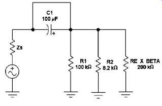
FIG. 7g Equivalent circuit of the AC signal input impedance of Fig. 7e.
The total equivalent impedance of the three parallel impedances of Fig. 7g (i.e., R1, R2, and beta _ RE) can be calculated using Eq. (5) of Section 2. (All of the fundamental laws and equations applicable to resistance values apply equally to impedance values.) In other words, the conductance value of each impedance is calculated, the three conductance values are summed, and the reciprocal of the sum is calculated. If you perform this calculation on the three parallel impedances of Fig. 7g, you should come up with approximately 7.3 Kohm. Therefore, from the perspective of the AC signal source, the entire circuit of Fig. 7e simplifies down to a simple series circuit, consisting of the AC signal source in series with its own internal impedance, which is in series with the 7.3-Kohm input impedance of the amplifier stage.
To understand the importance of considering the input impedance of typical transistor amplifiers, consider the following hypothetical circum stances. Suppose that the AC signal source of Fig. 7g has an internal impedance (Zs ) of 100 ohms, and the amplitude of the signal is 1 volt rms.
Under these conditions you have a 1-volt AC source in series with a 100 ohm impedance (Zs ) and a 7.3-Kohm impedance (the equivalent input impedance of the amplifier stage). Using the simple ratio method of calculating voltage drops (as detailed in Section 2), you will discover that only 13.5 millivolts would be dropped across the internal AC source impedance (Zs ), with the remaining 0.9865 volt applied to the amplifier stage. This example situation represents a good, practical impedance match, because over 98% of the AC signal source is applied to the amplifier stage.
In contrast, many AC signal sources, such as piezoelectric transducers or certain types of ceramic transducers, have very high internal impedances.
Looking at another hypothetical situation, suppose Zs in Fig. 7g were 100 Kohm, with the AC signal amplitude remaining at 1 volt rms. Again using the ratio method of calculating the AC voltage drops, you'll discover that about 0.932 volt will be dropped across the internal impedance of the AC signal source, and only 68 millivolts will be applied to the input of the amplifier stage. Since the amplifier of Fig. 7e provides a voltage gain of 10 (if the output is taken from the collector), the end result would be an "amplified" output voltage of only about 680 milli volts (i.e., 0.68 volt). In other words, your amplified signal is "lower" in amplitude than your original applied AC signal voltage! This condition results because the impedance of the AC signal source is not very compatible with the input impedance of the amplifier stage.
The procedure of insuring a practical and efficient impedance compatibility from one stage (or source) to another stage (or source) is commonly called impedance matching, or simply matching. The concept of impedance matching does not imply that two impedances are "equal." Rather, it denotes the fact that two impedances are properly chosen for the desired results. For example, the ideal situation for the maximum transfer of a voltage signal, as illustrated in Fig. 7e, is for the internal impedance of the AC signal source (Zs ) to be "zero," with the input impedance of the amplifier stage as high as possible. In this way, virtually "all" of the voltage is applied to the amplifier stage and none is lost across the internal impedance of the source.
FIG. 7h is an equivalent circuit illustrating the AC input impedance of the amplifier stage illustrated in Fig. 7f. Note that the parallel effect of R1 and R2 remained unchanged, but the incorporation of a bypass capacitor in Fig. 7f changed the base-emitter impedance as seen by the AC signal source. Since a capacitor typically looks like a short to an AC signal, incorporating C3 in Fig. 7f caused the emitter of Q1 to look as though it were shorted to circuit common. In other words, the AC signal no longer sees the effect of resistor RE. Therefore, in this case, the base-emitter impedance becomes the internal base-emitter junction impedance (called r' e ) multiplied by the beta parameter of the transistor;
r' e is typically approximated with the equation r' e
_ 25/I c , where I c
_ quiescent collector current in milliamps.
The quiescent DC base voltage established by R1 and R2 in Fig. 7f is approximately 2.2 volts. Subtracting the typical 0.7-volt drop across the base-emitter junction leaves about 1.5 volts across RE (remember, capacitor C3 looks like an open circuit to DC voltages, so the quiescent operating voltages are not affected by C3); 1.5 volts across emitter resistor RE indicates that about 1.5 milliamps of current is flowing through the emitter. Considering the base current to be negligible, this means that approximately 1.5 milliamps will be flowing through the collector as well. Using the previous equation to calculate r' , we obtain
r ' e
___ 16.67 ohms 25
_ 1.5 25
_ I
(Remember, I c must be in terms of "milliamps" for this calculation.)
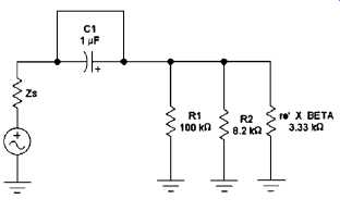
FIG. 7h Equivalent circuit of the AC signal input impedance of Fig. 7f.
If you look up a 2N3904 transistor in a data book, you'll discover that its typical beta (HfE ) parameter is about 200. Therefore, the base-emitter impedance of Fig. 7f will be r' e (16.67 ohms) multiplied by the beta (200), which equals about 3.33 Kohm. Now that all three parallel impedance values of Fig. 7h are known, you can calculate the equivalent impedance in the same manner as detailed for Fig. 7g. In this case, it comes out to about 2315 ohms, or about 2.3 Kohms.
If you recall, the AC input impedance for the transistor amplifier illustrated in Fig. 7e was 7.3 Kohm. By incorporating bypass capacitor C3, as illustrated in Fig. 7f, the AC input impedance was reduced to 2.3 Kohms. However, by incorporating the bypass capacitor (C3), the amplifier's AC voltage gain was greatly increased.
Thus far in this "transistor workshop," you have examined transistor fundamentals as they applied to signal amplification circuits. Transistors are also commonly used in various types of regulator circuits. Regulation is a general term applied to the ability to maintain, or "hold constant," some circuit variable, such as voltage or current. An older term synonymous with regulation is stabilization, which is still used commonly in some European countries (especially the United Kingdom).
FIG. 8a illustrates a constant-current source. As the name implies, constant-current sources provide a regulated current flow. In other words, the current flow is held at some constant level even though the resistance of the load varies greatly. Constant-current sources are of vital importance to a great variety of circuits, but their uses will be covered in later sections of this textbook. For now, only their theory of operation is discussed.
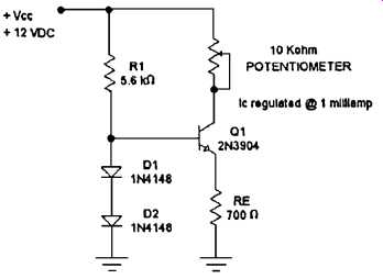
FIG. 8a An example of a simple constant current source.
Continuing to refer to Fig. 8a, note that diodes D1 and D2 are kept in a condition of continuous "forward bias" through resistor R1. As you may recall from Section 4, a silicon forward-biased diode will produce a reasonably constant voltage drop of about 0.7 volt, regardless of how much forward current it is passing. Since diodes D1 and D2 are held in a constant forward bias from the Vcc power supply (through R1), the base voltage of Q1 will be the sum of the two 0.7-volt drops, or approximately 1.4 volts DC. The base-emitter junction of Q1 will drop about 0.7 volts of this 1.4 volt base bias, leaving approximately 0.7 volts across RE. Therefore, using Ohm's law, the emitter current of Q1 is
I __ _ 0.001 amp or 1 milliamp 0.7 volt
__ 700 ohms E _ R
Of course, about 1/200th of this 1-milliamp emitter current will flow through the base (assuming that Q1 has a beta of 200), but if you consider this small base current to be negligible (which is appropriate in many design situations), you can say that about 1 milliamp of current must also be flowing through the collector. Note that the variable controlling the collector current flow is the constant voltage dropped across RE, which is held constant by the stable voltage drops across the two diodes.
In other words, the collector resistance has nothing to do with controlling the collector current. You should be able to adjust the 10-Kohm potentiometer (i.e., the collector resistance) from one extreme to the other with almost no change in the approximate 1-milliamp collector current flow.
You may want to construct the circuit of Fig. 8a for an educational experiment. If so, construct RE a 620-ohm resistor (700 ohms is not a standard resistor value-I chose this value in the illustration for easy calculation). If you don't have the 1N4148 diodes, almost any general purpose diodes will function well. When I constructed this circuit, our actual collector current flow came out to 0.9983 milliamps at the minimum setting of the potentiometer (I was lucky-actual results seldom turn out that close on the first try). By adjusting the potentiometer to its maximum resistance value, the collector current decreased to 0.9934 milliamps. This comes out to a regulation factor of 99.5% (i.e., the regulated current varied by only 0.5% from a condition of minimum load to maximum load), which is considered very good.
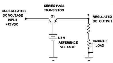
FIG. 8b An example of a simple "series-pass" voltage regulator.
Many types of electronic circuits require a very accurate and steady amplitude level of DC operational voltage. The problem with a simple "raw" (i.e., unregulated) power supply, such as the types discussed in Section 5, is that the output voltage(s) will vary by about 10-30% as load demands change. Consequently, voltage regulator circuits are needed to hold voltage levels constant regardless of changes in the loading conditions. FIG. 8b illustrates a simple method of maintaining a constant voltage across a load. A raw DC power source is applied to the collector of Q1, with a reference voltage source of 5.7 volts applied to the base. Allowing for the typical 0.7-volt drop across Q1's base emitter junction, about 5 volts should be dropped across the emitter load (think of the emitter load as being an emitter resistor, such as RE in Fig. 8a). For illustration purposes, a potentiometer is shown as a variable load in Fig. 8b. Note that the setting of the potentiometer does not control the voltage drop across the variable load. Rather, it is maintained at about 5 volts as a function of the constant 5.7 volts applied to the base of Q1 and the effect of Q1's beta, which tries to keep the emitter voltage equal to the base voltage (minus the 0.7-volt base-emitter drop). By adjusting the potentiometer, both the emitter current and the collector current will change radically in proportion to differences in the load resistance, but the voltage across the variable load will remain relatively constant. Because Q1 is connected in series between the raw DC power supply and the load, it is often referred to as a series-pass transistor.
At this point, you may be wondering why it is advantageous to incorporate Q1 in the first place. Why not simply provide operational power to the variable load directly from the stable reference voltage source? The answer to this very reasonable question is the simple fact that almost all high-quality sources of reference voltages have very limited output current capabilities. In other words, as soon as you begin to draw higher operational currents from the reference voltage supply, the voltage output will drop and it will cease to be a "reference voltage." Therefore, you need to make the reference voltage into a "controlling factor," while drawing the actual operational "power" from a different source. The regulator circuit of Fig. 8b utilizes the current amplification factor (beta) to control the "large" emitter-collector current flow with only a small base current flow provided by the reference voltage. In this way, the reference voltage and the voltage applied to the load remain stable, while the raw DC power supply provides almost all of the operational power to the load (i.e., almost all of the load current is provided by the raw power supply). For example, if you assume the beta parameter of Q1 to be 200, then the current requirements placed on the reference voltage will only be 1/200th of the actual operational current supplied to the load.
FIG. 8c illustrates how two transistors and a few passive components can be configured into a "voltage-regulated, adjustable DC" regulator. This type of regulator circuit allows you to adjust the level (or amplitude) of the DC output voltage with potentiometer P1. Once the output voltage is adjusted to the desired level, the regulator circuit will maintain this voltage level regardless of major variations in the load current (i.e., the voltage will be "regulated" at whatever level it is set to by P1).
The fundamental principle of operation for Fig. 8c is essentially the same as for Fig. 8b. That is, a reference voltage is applied to the base of the series-pass transistor (Q1) that is about 0.7 volt higher (in amplitude) than the desired voltage applied to the load. The raw DC power supply is connected to the collector of Q1, which will supply the majority of operational power delivered to the load. Transistor Q2, diodes D1 through D3, R2, and P1 form an "adjustable reference voltage" that is applied to the base of Q1, which, in turn, provides an "adjustable output voltage" at the emitter of Q1.
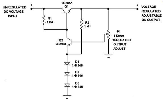
FIG. 8c More sophisticated adjustable voltage regulator circuit.
As a means of understanding the operation of Fig. 8c, imagine that Q2 and P1 are removed from the circuit, with the base of Q1 unconnected to anything except R1. Under these conditions, when the unregulated DC voltage is applied to the collector of Q1, the base-emitter current flow of Q1 will be forward-biased through resistor R1. The emitter voltage will rise to the same voltage as the unregulated DC voltage, minus a small drop across Q1. This is because the base of Q1 is at about the same voltage as the collector (the collector voltage is applied to the base by R1). The positive emitter voltage will forward-bias D1, D2, and D3 through R2. The voltage at the anode of D1 will be approximately 2.1 volts (0.7 volt + 0.7 volt + 0.7 volt = 2.1 volts; the three forward threshold voltages of the three diodes summed). As you recall, the for ward threshold voltage of a forward-biased diode is relatively "constant" regardless of the forward current flow. So the 2.1 volts produced by the forward-biased diodes serves the function of a "voltage reference," since the voltage drop across R2 nor the current flow through the diodes will alter this voltage by any great degree.
Now imagine adding P1 to the circuit of Fig. 8c. Since P1 is connected from the emitter of Q1 to circuit common, the voltage at the "tap" of the potentiometer can be at any level, from circuit common to the full emitter voltage, depending on how the potentiometer is adjusted. Finally, imagine that Q2 is now incorporated into the complete circuit as illustrated, with P1 adjusted to "tap off" about 50% of Q1's emitter voltage.
Under these conditions, when the unregulated DC voltage is applied to the collector of Q1, R1 will forward-bias the base-emitter junction of Q1, causing Q1's emitter voltage to begin to rise. As Q1's emitter voltage rises slightly above 2.1 volts, diodes D1, D2, and D3 go into forward conduction (through R2), applying about 2.1 volts to the emitter of Q2. As Q1's emitter voltage reaches a level of about 5.6 volts, the "tap voltage" of P1 is applying 2.8 volts to the base of Q2 (i.e., 50% of 5.6 volts is 2.8 volts). Since the emitter of Q2 is biased at 2.1 volts from the diode reference voltage source, and 2.8 volts is applied to its base by P1, the base of Q2 is now 0.7 volt "more positive" than the emitter, causing Q2 to begin to conduct. A type of balance occurs at this point. As the emitter voltage of Q1 tries to continue to rise, the voltage to the base of Q2 also rises, causing the collector-emitter current flow of Q2 to increase, which steals current away from the base of Q1 and restricts its emitter voltage from rising any higher than 5.6 volts. In other words, Q1's emitter voltage (which is the regulator's output voltage) is stabilized, or regulated, at this voltage level.
Now that the fundamentals of the circuit operation of Fig. 8c are understood, consider the effects of regulation when a hypothetical load is connected to its output. First, recognize that the conditions described in the previous paragraph applied to the no-load condition of the Fig. 8c circuit. In other words, no circuit or device of any type is drawing operational power from the output of the regulator. Now, assuming P1 to be left at its previous 50% setting (causing a regulated output voltage of about 5.6 volts), imagine connecting a 5.6-ohm resistor from the output terminal to circuit common. According to Ohm's law, if 5.6 volts is placed across a 5.6-ohm resistor, 1 amp of current will flow through that resistor. As soon as the load resistor is connected, the voltage at the output of the regulator will try to drop. However, as soon as it begins to drop, the voltage to the base of Q2 starts to drop also. This action decreases the collector-emitter current flow of Q2, causing an increase of base current to Q1, which, in turn, raises Q1's emitter voltage back to the balanced state of 5.6 volts. In other words, even with the extreme contrast of a no-load condition to a 1-amp load, the voltage output of the regulator circuit remained relatively constant. However, it is likely that the unregulated DC voltage applied to the collector of Q1 dropped by 1 or 2 volts.
A few final principles of the Fig. 8c circuit should be understood.
First, the regulated output voltage can be adjusted to any voltage level between the extremes of the reference diode voltage (i.e., 2.1 volts) and the level of the unregulated DC input voltage, by adjusting the setting of P1. However, regulation will become very poor when the output voltage level gets close to the unregulated input voltage level. Also, in the previous functional descriptions, I described voltages "rising, falling, trying to fall," and so forth. It should be understood that these changes take place in a few microseconds, so don't expect to see such actions without the assistance of a high-quality oscilloscope. And finally, there isn't any such thing as a "perfect" regulator circuit. When I constructed this circuit and adjusted P1 for a 5-volt output, there was a 0.3-volt drop in our output voltage from a no-load to a 1.5-amp loaded condition. By dividing the loaded voltage by the unloaded voltage, and then multiplying by 100, our percent regulation for this circuit came out to 94% regulation (4.7 volts divided by 5 volts _ 100 _ 94%). This regulation factor can be improved by utilizing transistors with higher HfE parameters.
If you would like to construct the regulator circuit of Fig. 8c, the raw DC power supply illustrated in Fig. 5-4 of the previous section will function very well as the unregulated DC voltage input source. SW1 and Rload in Fig. 5-4 would not be used for this application. Remember to properly "fuse-protect" the primary of T1. There will be one disadvantage to the completed power supply, however. If the load resistance goes too low, or if you accidentally short-circuit the output to circuit common, you will probably destroy the series-pass transistor, Q1. This is because there isn't any form of current-limit protection incorporated into the regulator circuit.
All common transistors have a maximum collector current parameter that cannot be exceeded without destroying the transistor. While common types of fuses can adequately protect many electrical and electronic devices (such as motors, transformers, and resistors), they cannot provide
"overcurrent" protection to transistors, because the transistor will be destroyed before the fuse has time to react. Also, in many situations a certain electronic application may require current limiting to a special type of load or circuit. For such applications, a rapid solid-state method is needed to freely allow current flow up to a limit, but restrict it at the limit if it tries to rise any higher. Such circuits are appropriately called current-limit circuits or current-limit protection.
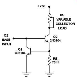
FIG. 8d A simple method of current limit protection.
FIG. 8d illustrates how a transistor (Q1) can provide current-limit protection for a transistor (Q2) or a load (RC). Assume, for example, you wanted to set the maximum collector current flow for Q2 at 10 milliamps. If you assume the base current to be negligible, you can view the emitter current as being approximately equal to the collector current (this is a reasonable approximation with high-beta transistors). At emitter current levels below 10 milliamps, the emitter-resistor (RE) voltage will drop to less than 0.7 volt, so the forward base-emitter voltage of Q1 cannot be obtained, and Q1 has no effect on the circuit. However, if Q2 reaches 10 milliamps of emitter current flow, the voltage drop across RE reaches the typical forward base-emitter voltage threshold of Q1 (i.e., 0.7 volt), initiating base-emitter current flow through Q1. As soon as some amount of base-emitter current flow begins, Q1 begins to promote a collector current equal to its beta parameter multiplied by its base current. Since Q1's collector current has to be provided by the base input to Q2, a certain portion of Q2's base drive current will be diverted to circuit common through transistor Q1, pulling the base input down to a level that will not cause more than 10 milliamps of emitter current flow through Q2. In other words, a current limit will occur when the voltage across RE reaches about 0.7 volt (corresponding to about 10 milliamps of emitter current flow, which also corresponds to about 10 milliamps of collector current flow). As the base drive current to Q2 tries to increase beyond this point, Q1 will divert more of the drive current to circuit common to maintain the 0.7-volt drop across RE. Within practical limits, the emitter current of Q2 can never exceed 10 milliamps. It should also be noted that the current flow through RC cannot exceed 10 milliamps, even if RC is reduced to zero ohms. Therefore, Q1 provides current-limit protection for both Q1 and the collector load of RC.
You may want to construct the circuit illustrated in Fig. 8d to experiment with. If so, RE can be 68 ohms (70 ohms is not a standard value) and you can place a 1-Kohm potentiometer (connected as a rheostat, as illustrated) in the collector circuit to act as a variable load. You can sup ply the base input to Q2 with a variable DC power supply or battery, but be careful not to allow the "base drive current" to exceed the maximum collector-current parameter of Q1. Otherwise, Q1 could be destroyed.
Although transistors with very high HfE (beta) parameters are avail able, in certain circumstances you may desire extremely high current gain factors. In these situations, a Darlington pair can be used (sometimes referred to as beta-enhanced pairs). FIG. 8e illustrates two common methods of producing a Darlington pair. In its simplest form, a Darling ton pair is created by simply connecting the emitter of one transistor to the base of a second, and connecting the two collector leads together.
This is illustrated in the left-hand illustration of Fig. 8e. Darlington pairs can be regarded and used, as though they were a "single" transistor with three leads, as illustrated. However, the beta parameter of the first transistor is multiplied by the beta of the second. In other words, if you made a Darlington pair out of two transistors, each having a beta value of 100, the Darlington pair would act like a single transistor with a beta of 10,000 (i.e., 100 _ 100 _ 10,000).
Unfortunately, there are a few disadvantages with Darlington configurations. Since the beta value is so extraordinarily high, complications with temperature instability may arise. A more temperature-stable Darlington configuration is shown in the right-hand illustration of Fig. 8e.
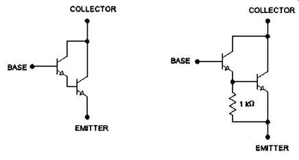
FIG. 8e Several examples of Darlington (i.e. beta enhanced) transistor
pairs. The circuit on the left is the more standard configuration, while
the circuit on the right provides improved DC and temperature stability characteristics.
However, by adding the temperature-stabilizing resistor, the base impedance of the Darlington pair is lowered considerably. Since the base input of a Darlington pair literally consists of "two" base-emitter junctions, the required forward threshold voltage is doubled (i.e., the base lead would have to be biased with about 1.4 volts for base-emitter current flow, instead of the normal 0.7-volt minimum for a single transistor). Depending on the type of circuit in which a Darlington pair is being used, there can be other problems as well. In high-frequency applications, the speed limitations of one transistor tends to add to the speed limitations of the second, making Darlington pairs relatively slow in comparison to single transistors. Also, with some critical circuitry, the apparent difference in the internal capacitances can adversely affect operation.
Final Comments
Even though the uses of transistors are quite varied, the basic fundamentals of transistor operation are quite simple. Within every circuit you have examined in this section, the actual transistor operation consisted of the following basics:
1. When the transistor was forward-biased, there was a 0.7-volt drop across the emitter-base junction.
2. The base current was multiplied by the beta (HfE ) parameter promoting a collector current flow equal to the product of the two.
3. The emitter voltage was the same as the base voltage, minus the 0.7-volt base-emitter voltage.
4. The "total" current flow through the transistor originated in the emitter, with a minor portion flowing through the base circuit, while the vast majority flowed through the collector circuit.
As you have seen, these basic operational characteristics of transistors can be manipulated into providing DC voltage amplification, AC voltage amplification, current regulation, voltage regulation, current limiting, and beta enhancement (i.e., Darlington pairs). These basic fundamental building blocks of transistor applications can be combined in various ways to provide a large variety of more complex functions and circuitry.
All of the circuits in this transistor workshop section have incorporated NPN transistors. PNP transistors can be used in the identical manner if all of the circuit voltage polarities are reversed.
Throughout this guide, I specify the "typical" forward threshold voltage of any forward-biased semiconductor junction as 0.7 volt. You may want to keep in mind that it is a little more technically accurate to consider this voltage to be 0.68 volt (i.e., 0.68 volt will be a little more accurate in the majority of cases). I elected to approximate this voltage at 0.7 volt for ease of calculation.
If this is your first reading of this section, I recommend that you now go back to the beginning of this section and study the entire con tents up to this point again. The information contained in this section is concentrated and quite abstract to most individuals on their first exposure to it. Don't become disheartened if you are confused on some points. Most of these fundamentals will become clearer during your second study, and most of your questions will probably be answered in later sections.
Assembly and Testing of Last Section of a Lab Power Supply
The following materials are needed to complete this section:
Quantity Schematic Reference Item Description
The fuse blocks and fuses are listed in case you want to fuse-protect the positive and negative outputs. This is a good idea, but it is not mandatory. The fuse blocks can be mounted in any convenient location prior to the binding posts. The fuse/fuse block assemblies are simply placed in series with the output wires going to the positive and negative binding posts (see Fig. 12).
FIG. 9 Examples of universal-type circuit boards that can be used to
permanently construct many projects within this guide.
FIG. 10 Examples of the most popular styles of insulated binding posts.
It might be a little difficult to obtain the series-pass transistors (Q1 and Q2) on a local basis. However, they are readily available through catalog suppliers.
Assembling the Circuit Board
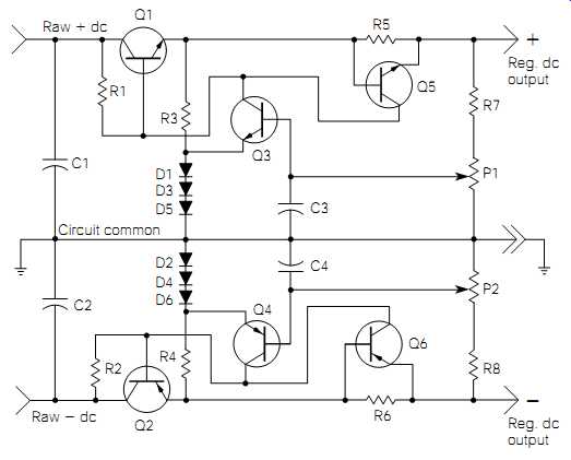
FIG. 11 Regulator section of the lab power supply project.
The specified grid boards are universal types, designed for building one of-a-kind circuits or prototypes. They consist of three-point solder pads and long strips, or rails, called "buses." Circuits are assembled using the three-point solder pads as connection points, and the bus lines are used for common connections to power supply voltages or circuit common.
To begin laying out the circuit board, refer to Fig. 11. The first step is to recognize that all of the components shown in the schematic will not be placed on the circuit board. C1 and C2 are already installed on solder strips connected to the chassis (this was performed in the last section). Q1 and Q2 will be externally mounted to the chassis bottom for heatsinking. P1 and P2 will be mounted to the front panel, as your voltage adjustment controls.
As the second step, notice how the positive regulator is almost a mirror image of the negative regulator (the circuitry above the circuit common line is the positive regulator; the negative regulator is below the circuit common line). Divide the grid board in half and concentrate on the positive regulator section first. On completion, the negative regulator is simply a duplication on the first half of the grid board.
By the time you have completed the prior steps, you are left with four resistors, two transistors, three diodes, and one capacitor (the circuit board mountable components for the positive regulator). It is not difficult to arrange these few components for proper connections (Fig. 11).
There is not a critical nature to these parts placements, so you might install them in any way that is easy and organized.
FIG. 12 Suggested physical layout for the finished lab power supply.
When you finish with the positive regulator section, copy the parts layout for the negative regulator. It is usually easier to wait until the entire circuit board is "populated" and double-checked, before permanently soldering any components into the board. Simply insert the components and bend the leads back to hold them in place temporarily. Don't forget to leave some empty holes in the pads for connecting the external components (Q1, Q2, P1, and P2) and the external wiring (raw DC inputs, regulated DC outputs, and the circuit common).
FIG. 12 shows a suggested method of physically mounting all of the components together with the circuit board. You might have to move things around a little to accommodate your enclosure. If you choose to fuse the outputs, the fuse blocks should be wired in series between the regulated DC outputs and the binding posts.
Regarding the external wiring to the circuit board, it should be stranded, 18- to 22-gauge insulated hook-up wire. An itemized list of the external wiring is as follows:
Three wires from the raw DC power supply (raw +DC, raw -DC, and circuit common) Three wires from Q1 (emitter, base, collector) Three wires from Q2 (emitter, base, collector) Six wires from P1 and P2 (three wires each) Three wires from the three binding posts (regulated +DC, regulated -DC, and circuit common) Mounting Q1 and Q2 Under worst-case conditions, Q1 and Q2 might have to dissipate close to 60 watts of power each. To keep them from overheating, some form of heatsinking must be provided. The chassis metal bottom will work nicely for this purpose, unless you try to operate the power supply in the current limit mode at low voltage, or if short-circuit conditions exist for extended periods of time. This worst-case condition could cause the series-pass transistors (Q1 and Q2) to overheat, even with the chassis heatsinking. Specially designed aluminum heatsinks can be purchased for the mounting of Q1 and Q2 to eliminate the problem, if desired.
When mounting Q1 and Q2 to the chassis, you will have to use an insulator (mica insulators are the most common for this purpose) to keep the transistors electrically isolated from the chassis. To aid in heat conductivity, the mounting surface of the transistor and the insulator is coated with a "thin" layer of thermal joint compound, commonly called "heatsink grease." Thermal joint compound is a white, silicon oil based grease used to fill the minute air gaps between the transistor, insulator, and heatsink material. Some power transistors require the use of an insulating sleeve to keep the mounting bolt from making electrical contact with the transistor collector. After mounting Q1 and Q2, use your DVM (in the "ohms" setting) to check for any continuity between the transistor's collector lead and the chassis. You should obtain an infinite resistance.
You might be wondering how you could check Q1 and Q2 during the power supply operation to know if they are getting too hot. Without the aid of expensive temperature measurement equipment, there is a very unscientific way to "guesstimate" possible temperature problems with semiconductors. Be sure that the power is off. Then, touch the transistors immediately after a period of operation. If they are too hot to comfortably hold your finger on them for more than 1 second, you should probably acquire some better heatsinking.
Circuit Description
The negative regulator functions identically to the positive regulator, except for the difference in voltage polarity. Therefore, I will detail only the operation of the positive regulator.
When power is first applied to the circuit, C1 charges to about 37 volts (as discussed in Section 5). R1 supplies sufficient base current to allow uninhibited current flow through Q1. As the Q1 emitter voltage approaches the "raw" DC level of C1, diodes D1, D3, and D5 all go into forward conduction through resistor R3. Once conducting, these diodes maintain a relatively constant reference voltage of about 2.1 volts, which is the sum of their individual forward threshold voltages.
As the Q1 emitter voltage continues to rise, it is applied to the R7 and P1 voltage divider. The P1 wiper is connected directly to the Q3 base. When the wiper voltage reaches about 2.8 volts, Q3 will begin to conduct. This occurs because the Q3 emitter is being held at 2.1 volts by the diode assembly, and its base has to be about 0.7 volt more positive than the emitter to overcome the forward threshold voltage requirement of the base to emitter junction. When Q3 starts to con duct, it begins to divert some of the current, being supplied by R1, away from the Q1 base. Consequently, Q1 begins to restrict some of its emitter-collector current flow. This leveling effect continues until the output is stabilized at a voltage output relative to the P1 setting.
When a load of some kind is placed on the output, the loading effect will try to decrease the output voltage amplitude. As the voltage starts to decrease, this decrease is seen at the P1 wiper and transferred to the Q3 base. Consequently, Q3 decreases its current conduction by an amount relative to the output voltage decrease. This allows more current to flow through the Q1 base, causing Q1 to become more conductive than it was previously. The end result is that the load is compensated for, and the output voltage remains stable (at the same amplitude as before the load was applied).
If a load is placed on the output, causing the current flow to exceed about 1.5 amps, the resultant current flow will cause the voltage drop across R5 to exceed the forward threshold voltage of the base-emitter junction of Q5. When Q5 begins to conduct, it diverts current flow away from the Q1 base, causing Q1 to decrease its current flow, and thus reduce the output voltage. The Q1-and-Q5 combination will not allow the output current to exceed about 1.5 amps, even under a short-circuit condition.
Testing the Power Supply
Before applying power to the power supply, set your DVM to measure ohms, and check for continuity of virtually every component to chassis ground. There is not a single part of this circuit that should be electrically connected to the chassis. If you measure resistance from any component to chassis ground, recheck your wiring and connections. Remember that you have a "floating" circuit common that is the power supply ground, but not connected to the chassis ground.
If you have double-checked your wiring, and are certain that every thing is correct, set P1 and P2 to their approximate center positions, and "pulse" the line power to the power supply on and off quickly. If there were no blown fuses, or other signs of an obvious problem (smoke, the smell of burning plastic insulation, or the "pop" of exploding plastic semiconductor cases), reapply the line power and measure the output voltages at the binding posts with your DVM. The positive and negative output voltages should be measured in reference to circuit common (the center binding post as illustrated in Fig. 12), not chassis ground. You should be able to smoothly adjust the positive output voltage by rotating P1 from a minimum of about 3.8 volts, to a maximum of about 36 volts. The negative regulated output should perform identically by rotating P2, except for the difference in voltage polarity.
In Case of Difficulty
If the power supply is blowing fuses on application of line power, you probably have a short-circuit condition on one of the raw DC supplies. Be sure that the line power is off, and disconnect the raw DC wires from the circuit board. Replace any blown fuses and apply line power. If you still blow fuses, the problem is most likely in the bridge rectifier (BR1). You learned how to check a bridge rectifier in Section 4.
It is most likely that the fuses won't blow after disconnecting the raw DC lines because the complete raw DC power supply was previously tested in Section 5. If this is the case, be sure that the line power is off, and use your DVM to measure the resistance from the collector of Q1 to circuit common. This should be a very high indication (our circuit measures over 2 Mohms). Make the same measurement from the Q2 collector. If either one of these resistance measurements are low, you have a wiring error or a defective component.
The most likely components to be defective in this circuit are the transistors and diodes. You have already learned how to test diodes with a DVM set to the "diode test" function. Transistors can be tested in this manner also.
Checking Transistors with a DVM
If a need arises to functionally test a bipolar transistor, it can be thought of as two back-to-back diodes. With your DVM set to the "diode test" mode, check the base-emitter junction just like any diode junction. The DVM should indicate infinity with one test lead orientation, while reversing the test leads will cause a low indication, or vice versa. Because a transistor is a two-junction device, you must perform the same test on the base-collector junction also. If both junctions appear to be functioning normally, you should measure the resistance from the emitter to the collector. This resistance should be high with both orientations of the DVM test leads.
To check transistors that have already been installed in a circuit, it is usually necessary to consider the parallel effects of other associated components that might influence the measurement. For example, in Fig. 11, the base to emitter measurement of Q5 will be predominantly influenced by R5. Because R5 is only 0.4 ohm, it will not be possible to measure the forward or reverse resistance of the base-emitter junction because 0.4 ohm is much less than either. In this case, you would need to temporarily disconnect the base lead before checking the transistor with a DVM. In some cases, it might be necessary to disconnect two of the transistor's leads to obtain a reliable test.
If you discover a defective transistor, there is a good chance that it was destroyed by an error in the wiring. After replacing the defective transistor, double-check its associated wiring for mistakes.