AMAZON multi-meters discounts AMAZON oscilloscope discounts
To this point, you have examined the application of diodes in only two general areas: rectification and volt age referencing (the three-diode voltage reference in the lab power supply project). There are many other applications, and numerous types of special-purpose diodes.
Optoelectronic devices are electronic devices used in applications involving visual indicators, visible light, infrared radiation, and laser technology. Special-purpose diodes make up a large part of this family.
Zener Diodes
Zener diodes are used primarily as voltage regulator devices. They are specially manufactured diodes designed to be operated in the reverse breakdown region. Every zener diode is manufactured for a specific reverse-breakdown voltage called the zener voltage (abbreviated VZ in most data books).
To understand the operational aspects of zener diodes, refer to FIG. 1. Note the symbol used to represent a zener diode. For this illustration, a 5.6-volt zener has been chosen. Assume that you can apply a vari able DC voltage to the positive and negative terminals of the circuit, ranging from 0 to 10 volts. Beginning at 0 volt, as the voltage is increased up to 5.6 volts, the zener diode behaves like any other reverse-biased diode. It totally blocks any significant current flow. And, because it rep resents an almost infinite resistance, the entire applied voltage will be dropped across it.
This all holds true up to the point when the applied voltage exceeds the rated zener voltage of the diode. When this avalanche voltage occurs, the zener diode will abruptly start to freely conduct current. The point at which this abrupt operational change occurs is called the avalanche point.
The minimum amount of current flow through the zener diode required to keep it in an avalanche mode of operation is called the holding current. The voltage across the zener diode does not decrease when the avalanche point is obtained, but it does not increase by a very significant amount as the applied circuit voltage is increased substantially. Hence, the voltage across the zener diode is regulated, or held constant.
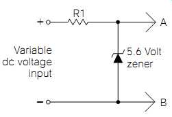
FIG. 1 Circuit demonstrating zener diode operation.
To clarify the previous statements, consider the circuit operation in Fig. 1 at specific input voltage levels. If 5 volts is applied to the input (observing the polarity as illustrated), the zener diode will block any significant current flow, because its avalanche point will not occur until the voltage across it reaches a level of at least 5.6 volts. If 6 volts is applied to the input, about 5.6 volts will be dropped across the zener, and about 0.4 volt will be dropped across R1. Increasing the applied input voltage to 7 volts causes the voltage across R1 to increase to about 1.4 volts, but the voltage across the zener diode will remain at about 5.6 volts. If the applied input voltage is increased all the way up to 10 volts, about 4.4 volts will be dropped by R1, but the zener diode will continue to maintain its zener voltage of about 5.6 volts. In other words, as the applied circuit voltage is increased "above" the rated voltage of the zener diode, the voltage across the zener diode will remain relatively constant and the excess voltage will be dropped by its associated series resistor, R1.
If a load of some kind were to be placed in parallel with the zener diode of Fig. 1, the zener diode would hold the voltage applied to the load at a relatively constant level, as long as the applied circuit voltage did not drop below the rated zener voltage of the zener diode.
The two most important parameters relating to zener diodes are the zener voltage and the rated power dissipation. Zener diodes are commonly available in voltages ranging from about 3 volts to over 50 volts. If a higher zener voltage is needed, two or more zener diodes can simply be placed in series. For example, if an application required the use of a 90-volt zener, this could be accomplished by placing a 51-volt zener in series with a 39-volt zener. Unusual zener voltages can be obtained in the same manner. Another method of obtaining an odd (nonstandardized) zener voltage value is to incorporate the 0.7-volt for ward threshold voltage drop of a general-purpose silicon diode. When using this method, the general-purpose diode is placed in series with the zener diode, but it is oriented in the forward-biased direction, and the zener diode is reverse-biased.
The standardized power dissipation ratings for zener diodes are 1/2, 1, 5, 10, and 50 watts. Zeners rated at 10 and 50 watts are manufactured in stud-mount casings, and must be mounted into appropriately sized heat sinks for maximum power dissipation.
Designing Simple Zener-Regulated Power Supplies
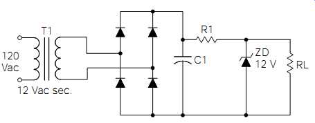
FIG. 2 Simple zener-regulated power supply.
Referring to Fig. 2, your design problem here is to build a 12-volt, 500 milliamp zener-regulated power supply to operate the load, designated as RL in the schematic diagram. Much of the "front end" of the circuit should be rather familiar to you by now. T1, the bridge rectifier, and C1 make up a raw DC power supply. (The methods of calculating the values and characteristics of these components will not be discussed in this context because this was covered in previous sections.) The design of a well-functioning zener-regulated power supply is a little tricky because of variations in the raw DC power supply. The out put voltage of a raw DC power supply may decrease by as much as 25% when placed under a full load. To roughly estimate the no-load voltage that C1 would charge to, the T1 secondary voltage should be multiplied by 1.414 to calculate the peak secondary voltage. In this case, the peak secondary voltage is about 17 volts. After subtracting about 1 volt to compensate for the loss in the bridge rectifier, you are left with about 16 volts DC across C1. Unfortunately, this calculation will be in error as soon as the power supply is loaded.
The primary component affecting the full-load voltage decrease of a raw DC power supply is the transformer. The percentage of full-load voltage decrease will depend on how close the full-load requirement comes to the maximum secondary current rating of the transformer.
For example, our hypothetical load in Fig. 2, as stated previously, will require up to 500 milliamps. If T1's secondary rating is 600 milliamps, the secondary voltage will decrease substantially when fully loaded.
However, if T1's secondary rating is 2 amps, the 500-milliamps full-load requirement of RL will have much less effect. In addition, even trans formers with similar ratings can behave somewhat differently, depending on certain manufacturing techniques.
A further complication, although not as dramatic, relates to the value of C1. When a load is placed on a raw DC power supply, the ripple con tent increases. A high ripple content has the effect of reducing the usable DC level.
The easiest solution to overcoming all of these unknown variables is to simply build the raw DC power supply, and place a dummy load across C1 that will closely approximate the full-load requirement of RL. In this case, you would start with the no-load voltage across C1, which is about 16 volts. Knowing that RL might require as much as 500 milliamps, the resistance value of the dummy load can be calculated using Ohm's law:
R __ _ 32 ohms 16 volts
_ 0.500 A E _ I
A 33-ohm resistor would be close enough for calculation purposes. But don't forget the power rating! This dummy resistor must be capable of dissipating about 8 watts.
Assume you built the raw DC power supply, placed the 33-ohm dummy load across C1, and measured the "loaded" DC voltage to be 14 volts. This gives you all the information you need to design the rest of the power sup ply. (You might have realized that when the raw DC voltage decreased under load, the 33-ohm dummy load no longer represented a full-load condition. Experience has shown that this "secondary" error, which is the difference between the "almost fully loaded" voltage and the "fully loaded" voltage, is not significant in the vast majority of design situations.) There are three variables you must calculate to complete your design problem: the power rating of the zener, the resistance value of R1, and the power rating of R1.
To calculate these variables, you need to understand how the circuit should function under extreme variations of RL. When RL requires the full load of 500 milliamps, the current flow through the zener diode should be as close to the minimum holding current as possible. Assuming the holding current is about 2 milliamps, that means about 502 milliamps must flow through R1; 2 milliamps through ZD, plus 500 milliamps through RL. R1 is in series with the parallel network of ZD and RL. The applied voltage to the series-parallel circuit of R1, ZD, and RL is the voltage developed across C1, which you are assuming to be 14 volts, under loaded conditions. Because 12 volts is being dropped across the parallel network of ZD and RL , the remaining 2 volts must be dropped by R1 (the sum of all of the series voltage drops in a circuit must equal the source voltage). You now know the voltage across R1, and the current flow through it. Therefore, Ohm's law can be used to calculate the resistance value:
R __ _ 3.98 ohms 2 volts
__ 0.502 amps E _ I
Of course, 3.98 ohms is not a standard resistance value. You don't want to go to the nearest standard value above 3.98 ohms because this would risk "starving" the zener diode from its holding current when the current flow through RL was maximum. The nearest standard value below 3.98 ohms is 3.9 ohms, which is the best choice. By using any of the familiar power equations, the power dissipated by R1 comes out to be about 1 watt. A 2-watt resistor should be used to provide a good safety margin.
The worst-case power dissipation condition for ZD occurs when there is no current flow through RL. If all current flow through RL ceases, the full 502 milliamps must flow through ZD. Actually, the maximum cur rent flow through ZD could be as high as 513 milliamps because you chose a 3.9-ohm resistor for R1 instead of the calculated 3.98 ohms. The power dissipated by ZD is the voltage across it (12 volts), multiplied by the current flow through it (the worst case is 513 milliamps). This is the familiar power equation P = IE. The answer is 6.15 watts. Therefore, ZD would need to be a 12-volt, 10-watt zener with an appropriate heatsink.
Another option would be to use two 5-watt, 6-volt zeners in series. The latter option eliminates the need for a heatsink, but care must be exercised to assure plenty of "air space" around the zener diodes for adequate convection cooling.
As the previous design example illustrates, zener-regulated power supplies are not extremely efficient because the zener diode wastes a significant amount of power when the current flow through the load is small. For this reason, zener-regulated power supplies are typically restricted to low-power applications. However, zener diodes are commonly used as voltage references in high-power circuits, as is illustrated later in this section.
Varactor Diodes
Going back to diode fundamentals, you might recall that when a diode is reverse-biased, a "depletion region" of current carriers is formed around the junction area. This depletion region acts as an insulator resulting in the restriction of any appreciable current flow. A side effect of this depletion region is to look like the dielectric of a capacitor, with the anode and cathode ends of the diode acting like capacitor plates. As the reverse-bias voltage across a capacitor is varied, the depletion region will also vary in size. This gives the effect of varying the distance between the plates of a capacitor, which varies the capacitance value. A diode that is specifically designed to take advantage of this capacitive effect is called a varactor diode. In essence, a varactor is a voltage-controlled capacitor.
Varactor diodes are manufactured to exhibit up to 450 pF of capacitance for AM (MW) radio tuning applications; but they are more commonly found in VHF (very-high-frequency) and UHF (ultra-high-frequency) applications, with capacitance values ranging from 2 to 6 pF. Virtually every modern television and radio receiver incorporates varactor diodes for tuning purposes, to reduce costs and to improve long-term performance by eliminating mechanical wear problems.
The schematic symbol used to represent varactor diodes is the same symbol used for general-purpose diodes, but with the addition of a small capacitor symbol placed beside it. FIG. 3 illustrates the commonly used electronic symbols for special-purpose diodes and optoelectronic devices.
Schottky Diodes
Schottky diodes are sometimes called "four-layer diodes" because their construction includes two layers of each type of semiconductor material.
The result is a NPNP device. As with all other types of diodes, they are two-lead devices.
The Schottky family of diodes includes the PIN diode, sometimes referred to as the silicon hot-carrier diode.
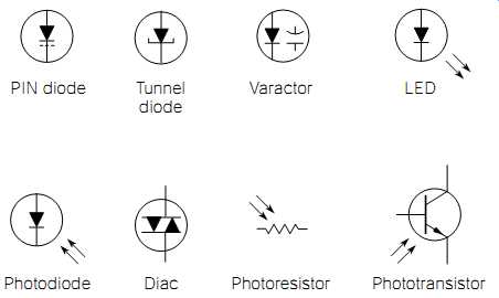
FIG. 3 Commonly used electronic symbols for special-purpose diodes and
photo-electronic devices.
These are breakdown devices, meaning that their useful function is to become highly conductive when the reverse voltage across them exceeds an inherent trigger voltage. Unlike zener diodes, they do not maintain their avalanche voltage across them after the trigger voltage has been reached. In contrast, their internal resistance drops to an extremely low value of only a few ohms, and remains there as long as a minimum holding current is maintained.
Schottky diodes are commonly used in high-frequency switching, detecting, and oscillator circuits.
Tunnel Diodes
Tunnel diodes are constructed similarly to ordinary diodes, with the exception of heavier impurity doping in the semiconductor material.
This results in an extremely thin depletion region under reverse-bias conditions and causes a tunnel diode to be a reasonably good conductor when reverse-biased. The unique characteristic of tunnel diode behavior, however, is in the forward-biased mode.
As the forward-biased voltage across a tunnel diode is increased, there will be three specific voltage levels where the tunnel diode will exhibit negative resistance characteristics. This means that the current through the tunnel diode will decrease as the voltage across it increases. As the forward voltage across a tunnel diode is smoothly increased from mini mum to maximum, the current response will show a series of three peaks and valleys as the tunnel diode vacillates between positive and negative resistance responses.
Tunnel diodes are used in oscillators and high-speed switching applications for digital circuitry.
Diacs
Diacs are three-layer bilateral trigger diodes. Like PIN diodes, diacs are breakdown devices. However, unlike PIN diodes, diacs are triggered from a blocking-to-conduction state in either polarity of applied voltage. Consequently, there are no band encircling around the device body to indicate the cathode end, because the orientation of the device is irrelevant.
For example, if the rated breakover voltage (the breakdown voltage, or avalanche point) for a specific diac is 30 volts, it will present an extremely high resistance until the voltage drop across it equals about 30 volts. At that point, it will become highly conductive; and it will remain in this state until the voltage across it reaches a minimum level. At that point, it becomes highly resistive again. It will react this way regardless of the voltage polarity; hence, it is bilateral in operation.
Diacs are most commonly used in high-power control circuitry to pro vide the turn-on pulses for silicon controlled rectifiers (SCRs) and triacs.
(SCR and triac operation will be discussed in a later section.) Diacs were designed to be a solid-state replacement for neon tubes.
Fast-Recovery Diodes
All diodes possess a characteristic called their recovery time, which is the amount of time required for the diode to turn off after being in the for ward conduction state. This is usually a very short time period; for 60-hertz rectification applications, recovery time is irrelevant. However, in high-frequency rectification applications, the recovery time becomes critical. For these applications, specially manufactured diodes with very fast recovery times are implemented. Logically enough, they are called fast-recovery diodes.
Noise and Transient Suppression Diodes
Common household and commercial AC power is fine for powering motors, heaters, and most electromechanical devices. However, in applications where AC power is used to provide the operational power for sensitive and high-speed solid-state circuitry, it can create many problems resulting from noise, voltage spikes, lighting surges, and other undesirable interference signals, which might be conducted into the home or industrial facility by the power lines. To help in eliminating these problems, a whole family of noise and transient suppression diodes have been developed.
Common names for such devices are unidirectional surge clamping diodes, varistor diodes, unidirectional transient suppression diodes, bidirectional transient suppression diodes, transorbers, and many others. All of these devices utilize the nonlinear resistive effect or the avalanche effect of semiconductor materials to reduce voltage spikes or overvoltage surges.
Their uses are primarily in solid-state power supplies and AC line filters.
A Basic Course in Quantum Physics
Light is a form of radiated energy. As such, it makes up a small part of the total range of radiated energies called the electromagnetic spectrum.
Radiated energy is composed of extremely small particles of wavelike energy called quantum (technically speaking, the plural form of quantum is quanta, but the effect of science fiction and media inaccuracy has brought quantum into the colloquial language). In reference to the visible and near-visible light frequencies, the older term quantum has been replaced with the newer term photon.
In the early days of solid-state electronics, it was discovered, quite by accident, that a solid-state diode would emit a small quantity of light as a side effect of the recombination process occurring in the PN junction, while forward-biased. This led to the development of the modern light emitting diode (LED). Further research led to the discovery that if an "out side" light source was focused on the junction area of a solid-state diode, the light photons had the tendency to "dislodge" some electrons from their atomic shell positions, resulting in an increase of "minority" carriers. In other words, the "leakage" current in a reverse-biased diode would increase proportionally to the light intensity falling on the junction.
This photoconductive property resulted in the development of the photodiode, the phototransistor, and the photoconductive cell. It is also possible to directly convert the energy of photons (light energy) into electrical energy. Devices capable of performing this energy conversion are called photovoltaic cells, or, more commonly, solar cells.
Further developments, involving a wider diversity of materials and manufacturing processes, led to the more recent member in the optoelectronic field: the laser diode. The term laser is actually an acronym for "light amplification (through) stimulated emission of radiation." As stated earlier, normal light consists of small "packets" of energy called photons.
The typical light emitted all around us consists of photons all traveling in random fashion and random frequencies. Laser light differs from nor mal light in several ways. First, it is "coherent," meaning that the photons are all traveling in the same direction. To understand this difference, consider a typical flashlight. As you shine a flashlight beam into a distance, the diameter of the beam of light will increase with distance, becoming very broad after only a hundred feet or so. In contrast, a laser light beam will not broaden with distance because all of the photons constituting the beam are going in the same direction. A high-coherency laser beam can easily be bounced off of the moon!
The second radical difference, between laser light and standard "white" light, relates to frequency. Solid-state semiconductor light-emitting devices, such as LEDs and laser diodes, typically emit only a narrow wave length of light. Therefore, the emitted light consists of only one "pure" color. Common white light, on the other hand, contains all of the colors (meaning all of the frequencies) in the visible light spectrum.
Now that most of the basic principles relating to optoelectronics have been defined, it is appropriate to discuss these devices individually, in more detail.
Light-emitting Diodes
A light-emitting diode (LED) is a specially manufactured diode that is designed to glow, or emit light, when forward-biased. When reverse biased, it will act like any common diode; it will neither emit light nor allow substantial current flow. LEDs can be manufactured to emit any color of the visible light spectrum desired, including "white" light. Red is, by far, the most common color. For certain physical reasons, semiconductor material is especially efficient and sensitive to near-visible light in the infrared region. Consequently, many photoelectric eyes used for presence detection and industrial control functions operate in the infrared region.
LEDs are used primarily as indicator devices. The brightness, or intensity, of an LED is relative to the forward current flow through it. Most LEDs are low-voltage, low-current devices, but more recent developments in optoelectronics have led to a family of high-intensity LEDs that approach the light intensity levels of incandescent bulbs.
Most commonly available LEDs operate in the 5- to 50-milliamp range and drop about 1.4 to 2 volts in the forward-biased mode. In most applications, LEDs require the use of a series resistor to limit the maximum current flow.
LEDs have far too many available case styles, shapes, and colors to describe in detail within this context, but each type will use some physical method to indicate the cathode lead. You will learn many of the indication methods through experience, but when in doubt, simply use your DVM in the "diode test" mode to check lead identification. (Most DVMs, in diode test mode, will cause an LED to glow very faintly when checked in forward-biased orientation.)
A common alphanumeric type of LED indicator device is the seven segment display. (The term alphanumeric refers to display devices capable of displaying some, or all, of the characters of the alphabet, as well as numbers.) Seven-segment LED displays are actually seven individual elongated LEDs arranged in a "block 8" pattern. Seven-segment LEDs will have a common connection point to all seven diodes. This common connection might connect all of the cathodes together (making a common-cathode display), or all of the anodes together (making a common-anode display).
The choice of using a common-cathode, or a common-anode display, is simply a convenience choice, depending on the circuit configuration and the polarity of voltages used. In addition, many types of "decoder" integrated circuits (integrated circuits designed to convert logic signals into seven-segment outputs), will specify the use of either common-cathode or common-anode displays.
A seven-segment LED will have eight connection pins to the case. One pin is the common connection point to all of the cathodes or anodes.
The other seven pins connect to each individual diode within the pack age. Thus, by connecting the common pin to the appropriate polarity, and forward-biasing various combinations of the LEDs with the remaining seven pins, any seven-segment alphanumeric character can be displayed.
Optoisolators, Optocouplers, and Photoeyes
Regarding their principles of operation, optoisolators, optocouplers, and photoeyes are equivalent; but their sizes, construction, and intended applications can vary dramatically. In essence, all of these devices consist of a light emitter (LED) and a light receiver (photodiode, phototransistor, photoresistor, photo-SCR, or photo-TRIAC).
The intensity of the light emitter can be varied proportionally to an electrical signal. The light receiver can convert the varying light intensity back into the original electrical signal. This process completely eliminates any electrical connection between emitter and receiver, resulting in total isolation between the two. Total electrical isolation is very desirable in circuits that could malfunction from electrical noise, or other interference signals, "feeding back" to the more susceptible areas. Light emitter receiver pairs used in this manner are called optical isolators (optoisolators) or optical couplers (optocouplers). The electrical signal being transmitted to the receiver might be either analog (linear) or digital (pulses).
These same basic components are often used in a photoeye mode. When used in this manner, the light emitter is held constant and sends a continuous beam of light to the receiver. The intended application requires an external object to come between the emitter and the receiver, breaking the beam, and thereby causing the receiver to produce a loss of-light signal. This type of "presence detection" is used extensively in VCRs, industrial control applications, and security systems.
Optoisolators and optocouplers utilizing a SCR or triac as the receiver are designed for AC power-control applications. The primary advantage in this configuration is the complete isolation from any noise or voltage spikes present on the AC line.
Photodiodes, Phototransistors, and Photoresistive Cells
Photodiodes are manufactured with a clear window in the case to allow external light to reach the junction area. When photodiodes are reverse biased in a circuit, the amount of "leakage" current allowed to flow through the diode will be proportional to the light intensity reaching the junction. In effect, it becomes a light-controlled variable resistor.
Photoresistors function much like photodiodes, but with a few differences. Unlike photodiodes, photoresistors are junctionless devices. There fore, like resistors, they do not have fixed orientation in respect to voltage polarity. Also, photoresistors react to light intensity with a very broad resistance range, typically 10,000 to 1. The typical "dark" resistance value of a photoresistor is about 1 Mohm; this resistance then decreases proportionally with exposure to increasing light intensity.
Phototransistors, like photodiodes, incorporate a clear window in the casing to allow ambient light to reach the junction area. The external light affects the transistor operation much like a base signal voltage, so in most cases, the base lead is left unconnected (some phototransistors don't even have base leads). Phototransistors are especially useful in some applications, because they can be used as amplifiers with external light either substituting for, or adding to (modulating), the base signal.
Laser Diodes
The widespread common use of coherent light in the average home has been made a reality by the solid-state laser diode. Every compact-disk (CD) player or CD-ROM (read-only memory) system utilizes a laser diode as the light source for reading the disk data. The commonly seen " laser pointers," familiar to office environments, are little more than a laser diode and a couple of batteries enclosed in a case.
Laser diodes are actually a type of LED. Their operation is similar; the primary difference is in the type of light emitted. Laser diodes emit coherent light.
Laser diodes are available in power ranges from about 0.5 to 5 mW.
They are also available as visible red or infrared emitters.
NOTE Please use caution if you plan to use or experiment with laser diodes.
Laser light is dangerous to the eyes. Always follow the manufacturer's recommended safety precautions.
Liquid-Crystal Displays
Liquid crystal displays (LCDs) have rapidly replaced LED systems in many indicator applications because of several advantages. First, LCDs require much less operational power than do comparable LED systems. This is because LCDs do not actually produce any light of their own; LCD operation depends on ambient light for character display. The second LCD advantage relates to the first. Because LCDs depend on ambient light for operation, they are the most visible in the strongest light where LEDs often appear faint.
An LCD is an optically transparent sandwich, often including an opaque backing. The inner surfaces of the panels making up the sandwich have a thin metallic film deposited on them. On one of the panels, this film is deposited in the form of the desired characters or symbols to be displayed. The space between the two panels contains a fluid called nematic liquid. This liquid is normally transparent. When an electric field is placed between the back panel and the desired character to be displayed, the liquid turns black and is displayed, provided that the ambient light is strong enough to see it. This is really no different than using a black magic marker to write a character on a piece of white paper; such a character is clearly visible in normal light, but you couldn't see it in the dark.
Although research is continuing in the LCD field, to date, there are some severe disadvantages. For one, LCDs are much slower than LEDs, making their use in high-speed display applications (such as television) limited.
Their speed of operation is greatly affected by temperature; operation becomes visibly slow in cold temperatures. Another disadvantage is versatility. LCD displays must be manufactured for specific applications. For example, an LCD intended for use as a clock display could not be used as a counter display because the colon, which normally appears between the hour and minute characters, places an undesired space between the numerals. After an LCD is manufactured, its character display cannot be modified for another application. A third disadvantage, relating to the home hobbyist or experimenter, is the decoding required for correctly displaying the characters. It could be very complex, requiring ICs that might not be readily available. If you plan on ordering LCD displays from any of the surplus electronics suppliers, be sure that it includes all of the necessary interface documentation.
Charge-Coupled Devices
Charge-coupled devices (CCDs) are actually digital circuits used primarily to replace the older "vidicon" tubes in video cameras. They require less power to operate and provide a much sharper and clearer picture.
Although CCDs are currently used exclusively for video "reception," research toward using CCD technology for solid-state display applications is very promising.