AMAZON multi-meters discounts AMAZON oscilloscope discounts
(cont. from part 1)
Circuit Project!
As an electrical engineer, instructor, and amateur scientist, I have come to fully appreciate the electronics field as being one of infinite creativity and infinite possibilities. As I write the text for this guide, I am surrounded by devices that would have been considered incomprehensible miracles only a few decades ago. Currently, scientists are taking the first infantile steps toward uncovering the mysteries of subatomic structure and quantum physics. These areas of research could lead to gravity and anti-gravitational generators, total annihilation fusion reactors, and deep space travel by means of bending the time-space continuum! Virtual reality systems are available today that can positively knock your socks off! Does all this sound a little more than mildly interesting?
Although I can't show you how to build a time machine, this section, together with the concurrent Circuit Project sections, contains a collection of projects and circuit building blocks that can be practical, fascinating, and fun (with the emphasis on "fun"). This particular section allows you to start taking the first steps toward discovering all of the creative and ingenious facets within your own self. I'm hoping someday you'll be able to show me how to build a time machine.
I suggest that you read through the description of each circuit even if you do not intend to build or experiment with it. The practical aspects of much of the previous theory is illustrated within them.
Preliminary Steps to Project Building
At this point, I am assuming that you have a lab power supply, DVM, electronic data books, soldering iron, hand tools, suppliers for electronic parts, and miscellaneous supplies needed for project building. In addition, I highly recommend that you purchase a solderless breadboard for testing the following projects before permanently building them. A solderless breadboard is a plastic rectangular block with hundreds, or thou sands, of contact points internally mounted. Electronic components and interconnection wiring (ordinary no. 22 solid-conductor insulated wire) are simply inserted into the breadboard (without soldering), and the completed circuit can be tested in a matter of minutes.
The circuit can then be modified by simply unplugging the original components and inserting new ones, until the operation is satisfactory.
At this point, the user can then remove the components of the perfected circuit, and permanently install them in a universal perfboard or PC board. The solderless breadboard is not damaged in this process, and it can be used repeatedly for designing thousands of additional circuits.
An illustration of some excellent-quality solderless breadboards is given in Fig. 4. You can also buy pre-stripped, pre-bent hook-up wire intended for use with solderless breadboards. For the modest cost involved, I believe this is a good investment.
Flashing Lights, Anyone?
FIG. 5 illustrates a good basic circuit to cause two LEDs to spontaneously blink on and off. The frequency will be about 1 Hz, depending on component tolerances and the type of transistors used.
The basic circuit is called an astable multivibrator. Multivibrators are covered in more detail in successive sections, but for now you can think of it as a free-running oscillator.
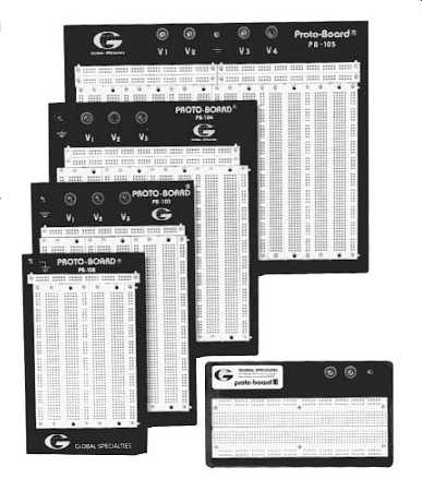
FIG. 4 Examples of solderless breadboards.
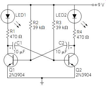
FIG. 5 A dual-LED flasher.
When power is first applied to this circuit, one transistor will saturate (the state of being turned on fully) before the other because of slight component variations. For discussion, assume that Q1 saturates first. In the saturation state, Q1 conducts the maximum collector current lighting LED1. At the same time, this condition makes the positive side of C1 appear to be connected to ground, and it begins to charge to the supply potential through R3. When the charge across C1, which is also the base voltage of Q2, charges to a high enough potential, it causes Q2 to turn on and lights LED2.
At the same time, the positive side of C2 is now placed at ground potential, causing the base voltage of Q1 to go low, forcing Q1 into cut off (the state of being fully turned off). With Q1 at cutoff, LED1 is dark and C1 begins to discharge back through R3. In the meantime, C2 is now charging and applying a rising voltage to the base of Q1. This continues until Q1 saturates again, and the whole process starts over again.
(You might have to slowly reread this functional description and study Fig. 5 several times to fully grasp the operation.) The astable multivibrator shown in Fig. 5 is certainly a basic building block for many future applications. Here are a few examples of how this circuit could be modified for a variety of projects. The frequency and on-time/off-time relationship (called the duty cycle) can be changed by changing the values of C1, C2, R2, and R3. Experiment with changing the value of each of these components, one at a time, and observe the results. R2 and R3 can be replaced with rheostats (potentiometers connected as variable resistors) for continuously variable frequencies and duty cycles. C1 and C2 can be replaced with smaller values of capacitance making the circuit useful as a simple square-wave frequency generator. With the correct choice of transistors and capacitors, this circuit is usable well into the megahertz region. If you wanted to flash brighter lights, LED1 and LED2 could be replaced with small 6-volt relay coils. The relay contacts, in turn, could be connected to the line voltage (120 volts AC), and incandescent lamps for high-brightness flashing (be careful not to exceed the contact current and voltage ratings of the relays). There are many more applications. The fun is in using your imagination.
Three Lights Are Better than Two!
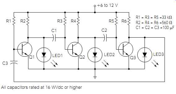
FIG. 6 A triple-LED flasher circuit. All capacitors rated at 16 WVdc
or higher
FIG. 6 illustrates a variation of the same circuit illustrated in Fig. 5.
The primary differences are that the LEDs will light when their associated transistor is in cutoff, rather than saturation, and an extra transistor circuit has been added for a sequential three-light effect.
Only one transistor will be in the cutoff state at any one time.
Assume that transistors Q1 and Q3 are saturated, and that Q2 is cutoff.
In this state, LED2 is bright from the current flow through Q2's 560 ohm collector resistor. Meanwhile, C1 is charging through Q2's 33-Kohm base resistor. When the voltage across C1 reaches a high enough potential, it turns on Q2 and causes LED2 to become dark (the saturation of Q2 effectively short-circuits the voltage drop across LED2).
Here is where the circuit operation becomes a little tricky. Going back to the prior condition when Q2 was in cutoff, the voltage on the negative side of C2 was actually a little more positive than the voltage on the positive side. This is because the voltage drop across LED2 was a little higher than the base-to-emitter voltage drop of Q3. Therefore, C2 actually takes on a slight reverse voltage charge. When Q2 saturates, this has the effect of forcing Q3 into "hard" cutoff, because a slight negative voltage is applied to its base, before C2 has the chance to start charging in the positive direction through Q3's 33k base resistor. With Q3 in the cutoff state, C3 begins to take on a small reverse charge, while C2 begins to charge toward the point where it will drive Q3 back into saturation. The cycle continues to progress in a sequential manner, with LED1 lighting next, and so on. Even though C1, C2, and C3 are electrolytic capacitors, the small reverse charge is not damaging because the charging current and voltage are very low.
The frequency of operation is a function of the time constant of the capacitors and base resistors. Increasing the value of either component will slow down the sequence. Any general purpose NPN transistor should operate satisfactorily in this circuit. The LED type is not critical, either, although you would have to adjust the resistor values somewhat to accommodate the newer "high brightness" LEDs.
Many of the applications that applied to Fig. 5 will also apply to this circuit. One of the advantages of this circuit design is that additional transistor stages can be added on for a longer sequential flashing string.
A Mouse in the House
FIG. 7 is definitely a "fun" circuit. It consists of two astable multivibrator circuits, very similar to the circuit in Fig. 5. The first multivibrator circuit will oscillate very slowly, because of the component values chosen. However, the second multivibrator circuit, consisting of Q3 and Q4, will not oscillate until Q2 saturates, which will occur every few seconds. The component values for the second multivibrator are chosen so that it will oscillate very rapidly and produce a "chirping" or "squeaking" sound if a small speaker is connected to it.
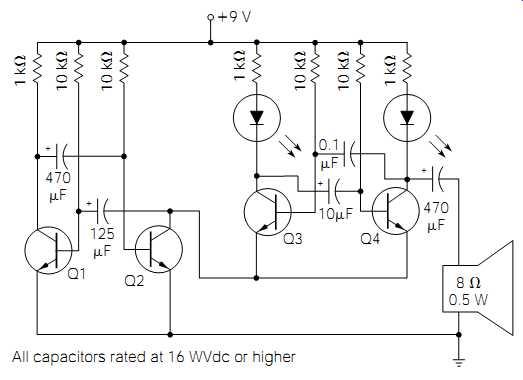
FIG. 7 An electronic chirping circuit. All capacitors rated at 16 WVdc
or higher
This circuit can be assembled on a very small universal perfboard and enclosed in a small plastic project box together with the speaker, an on-off switch, and a 9-volt transistor battery (which powers it nicely).
The two LEDs are optional, but their effect is dramatic.
Once completed, it should be about the size of a pack of cigarettes. It can easily be put in your pocket and carried to a friend's house. When the opportunity arises, turn it on and hide it somewhere inconspicuous.
Then, wait for the fun to start! The chirping sounds like a mouse, or some type of large insect. It is not loud enough to cause instant attention, but everyone in the room will notice it in a few minutes. The frequencies and harmonics produced by the multivibrator have the effect of making the sound omnidirectional, so it will be difficult to locate. In the meantime, everyone who is a little squeamish toward mice or large insects will get seriously nervous.
It is important to use a very small speaker for this project to achieve the desired effect. Virtually any type of general-purpose NPN transistors will perform well.
If you would like to try a variation on this circuit to produce some really weird sounds, try replacing Q1 and Q3 with a couple of three-lead phototransistors. Connect the phototransistors into the circuit exactly like the original transistors. This causes the changes in ambient light to "sum" with the original base voltages. Various capacitor and resistor combinations will produce some remarkable sounds in conjunction with changing light intensities.
To carry this idea one step further, you can mount this circuit in the center of a bull's-eye target and convert a laser pointer into a "gun" (put a dummy handle on it, and fabricate the on-off switch into a trigger). Using various component values, the target can be made to pro duce any number of strange sounds, when the laser beam hits the bull's-eye. Including a small power amplifier into the circuit, to boost the output volume, will improve the effect. If you built multiple circuits, adjusted them for individual sound effects, and mounted them in a variety of targets, you could have a high-tech shooting gallery in your own home!
A Sound Improvement
FIG. 8 is a Hi-Z (high-impedance) audio amplifier circuit that will greatly increase the volume level of a high-impedance headphone (two of these circuits will be needed for stereo headphones). This circuit can come in handy if you want to use your headphones to listen (loudly!) to some of the sounds that you can create with these multivibrator circuits.
The input impedance is high enough to keep it from loading down most circuits. You can also use this circuit with most types of speakers that have an impedance-matching transformer connected to the speaker frame. Don't try to use a standard 8- or 4-ohm speaker; you'll destroy the transistor, or the speaker, or both! This circuit is a modified form of the common-emitter transistor amplifier discussed in Section 6. VR2 should be adjusted for the best quality of sound, and VR1 is the volume control.
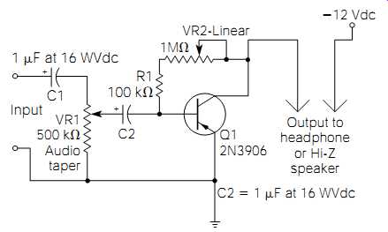
FIG. 8 High-impedance headphone amplifier.
A Delay Is Sometimes Beneficial
In the field of electronics, there are many control applications that require a time-delay relay (TDR). Commercial TDRs are very expensive.
FIG. 9 is a time-off TDR, which is both useful and inexpensive. It can also be modified for a variety of functions. Q1 and Q2 are connected in a configuration called a Darlington pair.
The Darlington pair configuration is essentially a beta multiplier, causing the beta value of Q1 to be multiplied by the beta value of Q2. For example, if both transistors had a beta value of 100, the overall beta value for the pair would be 10,000. The high beta value is particularly useful in this circuit, because only an extremely small Q1 base current is needed to saturate the pair. A discussion of the circuit operation will illustrate why this is important.
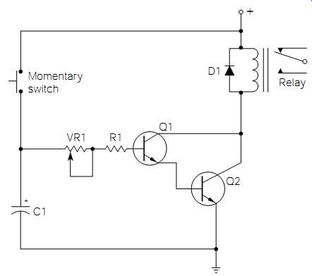
FIG. 9 Time-off delay relay driver.
When the momentary switch is closed, C1 will appear to charge instantly, because there is no significant series resistance to limit the charge rate. At the same time, Q1 is supplied with more than enough base current to saturate the transistor pair, and the relay is energized.
When the switch is released, opening the charge path to C1, C1 begins to "slowly" discharge through the Q1-Q2 base-emitter circuits. Because very little base current is needed to keep the transistor pair saturated, VR1 and R1 can be of a high resistance value, causing a very slow discharge of C1. The majority of C1's discharge cycle will maintain the saturated condition of Q1 and Q2, causing the relay to remain energized for a substantial time period after the switch is released. Theoretically speaking, if you tried to perform this same function with only a single transistor, the resistance values of VR1 and R1 would have to be about 100 times smaller to maintain a base current adequate for saturation (assuming both transistors to have a beta value of 100), and the discharge rate of C1 would be very rapid. You could accomplish the same operation if you increased the value of C1 by a factor of 100, but large electrolytic capacitors are both expensive and bulky.
FIG. 9 is a time-off TDR, meaning that after the control action is instigated (closing and releasing the momentary switch), there is a time delay before the relay deenergizes. The length of the time delay depends on the setting of VR1, which largely controls the discharge rate of C1.
This circuit can be easily modified to provide a time-on/time-off delay.
Remove VR1 and connect the opened end of R1 to the positive side of C1. Then connect VR1 into the C1 charge path, between the momentary switch and the applied power source. In this configuration, when the momentary switch is closed, C1 must charge through VR1, causing a time-on delay, until C1 charges to a high enough potential to cause the transistor pair to saturate. The length of this delay would depend on the setting of VR1. On releasing the momentary switch, a time-off delay would occur, while C1 is discharged through R1 and the base-emitter junctions of Q1 and Q2. This delay would be largely controlled by the value of R1.
If you wanted a time-on TDR (without the time-off function), a reasonably good facsimile can be made by simply removing R1, and by connecting the base of Q1 directly to the positive side of C1. Connect R1 in series with VR1 in the C1 charge path. By experimenting with different values of VR1 and C1, a significant time-on delay can be achieved with a fairly rapid turn-off.
Q1 and Q2 are general-purpose NPN transistors. For best results, use low-leakage-type transistors. The voltage amplitude of the circuit power source should be about equal with the relay coil voltage. For experimentation purposes, start with a C1 value of about 100 uF, and an R1 and VR1 value of 100 Kohms and 1 Mohm, respectively. These values can then be adjusted to meet your requirements. Whenever relay coils are incorporated into DC-powered solid-state circuitry, they should always be paralleled with a reverse-biased general-purpose diode. Note the orientation and connection of D1 in Fig. 9. The purpose of D1 is to sup press the inductive kickback, transient voltage spike, which will occur when the relay is deenergized. This kickback voltage spike can easily damage solid-state devices. It is generated by the stored energy in the electromagnetic field surrounding the relay coil. Fortunately, these voltage spikes will always be in the opposite polarity of the applied power source. Therefore, D1 will short out the spike, and render it harmless.
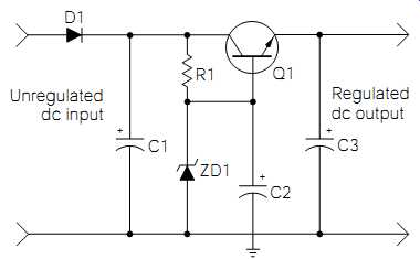
FIG. 10 A series-pass regulator using a zener diode as a voltage reference.
A Long-Running Series
Earlier in this section, during the discussion of zener diode regulators, it was shown why zeners are not very power-efficient as high-current regulators. A circuit designed to greatly improve the efficiency and operation of voltage regulation is illustrated in Fig. 10.
Much of this circuit should already be familiar to you. D1 is needed only if you plan on using this regulator circuit with a battery as the unregulated power source. C1 is the filter capacitor(s) for the raw DC power supply. This raw DC power supply can be of any design you choose. R1 and ZD1 form a simple zener regulator, as discussed previously in this section. However, in this circuit, the zener serves as a voltage reference for the series-pass transistor Q1. Transistor Q1 serves as a current multiplier for the zener. For example, if Q1 has a beta value of 100, and the current requirement for the load is 1 amp, the zener would only have to supply 10 milliamps of current to the base of Q1 for a 1-amp output.
This means that the value of R1 can be chosen so that the current flow through ZD1 is only slightly above its minimum holding current.
Therefore, ZD1 is only required to dissipate a small quantity of power, and a much higher load can be regulated (remember, a "high" load means that the load resistance is "small," and vice versa). C3 serves as an additional filter for smoothing the regulated DC.
For regulating most low-voltage loads requiring up to about 1 amp, ZD can be a 1-watt zener. Its zener voltage value should be 0.6 volt above the desired regulated output voltage. Q1 will drop this 0.6-volt excess across the base to emitter junction. For example, if you wanted a 5-volt regulated output, ZD should be a 5.6-volt zener. The value of R1 should be chosen to place the zener diode at about 15 to 20 milliamps above its rated holding current. Commonly used transistors for Q1 are the TIP31, TIP3055, and 2N3055 types.
Capacitor C2 serves a unique purpose in this circuit. Connected as shown, transistor Q1 serves as a capacitor multiplier, multiplying the filtering effect of C2 by its beta value. If capacitor C2 had a value of 1000 uF and Q1 had a beta of 100, the regulated output voltage would be filtered as if a 100,000-uF capacitor had been placed in parallel with the output.
Keep It Steady
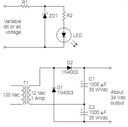
FIG. 11 Regulating the current flow through an LED.
FIG. 12 A voltage-doubler rectification circuit.
You will probably run into many situations where you will want to use an LED as an indicator for a variable-voltage circuit. Trying to use a single resistor for current limiting will prove ineffective for this application because the current flow through the LED will vary proportionally to the voltage, and it is likely to go too high, or too low, for good results.
FIG. 11 is a quick and easy solution to the problem. A low-power zener (ZD1) will maintain the voltage across the resistor-LED combination at a relatively constant level, regulating the current flow through the LED, and the voltage variations will be dropped across R1.
Double Your Pleasure
Do you have a transformer in your junk box that you would like to use for a circuit application, but the secondary voltage is too low? If so, you can use the voltage-doubler circuit illustrated in Fig. 12 to approximately double the secondary output during the rectification process.
In Fig. 12, a transformer with a 12-volt, 1-amp secondary is used to illustrate this principle. D1 and D2 are configured as two half-wave rectifiers, and C2 and C1 are their associated filters. C1 and C2 are simply connected so that their voltages are additive.
Capacitors C1 and C2 filter a half-wave rectified voltage, so they must have a much higher capacity that do comparable capacitors used for full wave filtering. D1 and D2 are common, general-purpose diodes. Also notice that neither secondary transformer lead is used as the common reference.
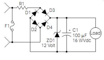
FIG. 13 An electronic fuse monitor circuit.
Show the Blow
As our last entry into this section of circuit Project, I submit the blown fuse alarm circuit illustrated in Fig. 13. In most homes, there are situations where it is critical to maintain electrical power to certain devices. For example, a chest freezer or a sump pump located in the basement have critical needs for constant power. A blown fuse (or tripped circuit breaker) to either of these appliances could result in a flooded basement, or the loss of hundreds of dollars' worth of food.
Unfortunately, it is likely that the blown fuse will not be discovered until the damage has already occurred. The circuit shown in Fig. 13 solves that problem by providing an alarm when a blown-fuse condition occurs.
When a fuse blows, it represents an infinite resistance (like an open switch) within an electric circuit. Therefore, the entire source voltage for the circuit will be dropped across it. This is how the fuse-monitoring circuit obtains its operational power.
Assume that the fuse (F1) is protecting a 120-volt AC circuit (I do not recommend this monitoring circuit for AC voltages higher than 120 volts AC). On blowing, it will apply 120 volts AC to the monitor circuit.
R1 limits the current, and drops most of the applied voltage. Diodes D1 through D4 rectify the voltage and apply pulsating DC to the zener diode (ZD1). C1 filters the pulsating DC to apply smooth DC to the load.
The load can be a piezo buzzer (such as used in smoke detectors) or any other type of low-power, low-voltage visible or audible indicator.
The resistance value and power rating of R1 will depend on the load requirement. Build the circuit as illustrated using a 1-amp, 200-volt PIV bridge rectifier (or comparable diodes), a 1-watt zener diode, and a 100 Kohm, 1/2-watt resistor for R1. If the load will not operate when 120 volts AC is applied to the circuit, start decreasing the value of R1 a little at a time until you reach the point of reliable operation. If reliable operation requires going below 12 Kohms, I suggest you try using an indicator requiring less operational power. At R1 values lower than 68 Kohms, the power rating should be increased to 2 watts.
This circuit can also be used to monitor fuses used in DC circuits.
For these applications, the bridge rectifier is not required, but be sure to observe the correct polarity.
The enclosure for this circuit will depend on the intended application. For instance, 120-volt AC applications require the use of an "approved" metal enclosure, properly grounded, and with wiring and conduit meeting national and local safety standards. It might also be necessary to fuse-protect the monitor circuit.
A final word of caution:
Please don't try to connect this circuit into a fuse box or breaker box, unless you're fully qualified to do so. Mistakes resulting from a lack of knowledge or experience in this area can result in property damage, fire hazard, and electrocution (especially if you're working on a damp basement floor)!