AMAZON multi-meters discounts AMAZON oscilloscope discounts
WE are now in the happy position of a contractor who arrives on the scene and finds all his building materials on hand. We can start the labors of this section with the two diodes shown in Fig. 301. Here we have a pair of p-n diodes (we could call them n-p diodes just as correctly) and we have placed them so that the two n-sections are in close contact.
Our two n-sections, though, are fairly identical, so there is no reason why we cannot have one single block of n-type germanium instead of separate pieces. Fig. 302 shows our new arrangement.
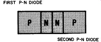
Fig. 301. Our first step toward the transistor is to use a pair of p-n
diodes back to back.
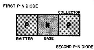
Fig. 302. We still have a pair of p-n diodes but we have now joined
the two n-sections into a single unit.
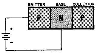
Fig. 303. With the positive terminal of the battery connected to p-type
semiconductor and the negative terminal to n-type, we have forward-biased
the diode.
Other than the unification of the n-section (and that was no radical move) we have made no changes whatsoever.
What do we have now? Just three blocks of germanium-some what giving rise to the idea of a sandwich, but rather more difficult to manufacture. However, two of our blocks are still identical, so to keep from compounding confusion, let's give them names. The one at the left is called the emitter, the one at the right the collector, and ·separating the two is the base. This is a transistor, and just as we informed you earlier, it can be regarded as a pair of diodes placed back to back.
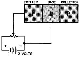
Fig. 304. In this case, the forward biasing can be varied from zero
to a maximum of 2 volts.
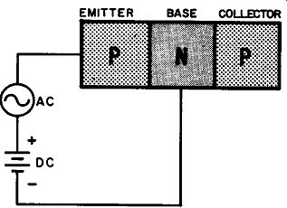
Fig. 305. Instead of using a potentiometer to change the amount of forward
biasing, we can use a signal voltage, represented here by the symbol
for an ac generator.
Biasing the transistor
As long as diodes are separate entities they have a sort of independence. Consider the transistor in Fig. 302, though. How do we bias it? We can connect a battery between the base and the emitter. We can immediately recognize this (in Fig. 303) as for ward biasing, since the plus terminal of the battery connects to the emitter (p-type germanium) and the minus terminal to the base (n-type germanium). Disregarding the collector for the moment, we have a single forward-biased diode.
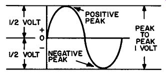
Fig. 306. Both the positive and negative halves of an ac input have
an effect on the forward biasing.
Changing the bias
Our forward bias battery is connected between the base and the emitter. Changing the bias is no great problem, since we can follow exactly the same techniques described earlier in Section 2.
The idea is repeated in Fig. 304. Adjusting the moving arm of the potentiometer gives us any value of bias we want, within the voltage limits of our battery. In the drawing of Fig. 304 we are assuming a battery voltage of 2.
We have another technique for varying the bias, although it may not be so readily apparent. The technique is illustrated in Fig. 305. Here we have an ac voltage source in series with the battery. What is this voltage? It could be supplied by a trans former, a signal generator, or it could be a broadcast signal. But regardless of how we obtain it, suppose we assume that the voltage has a peak-to-peak value of I. This means that the maximum positive peak is one-half volt. Similarly for the maximum negative peak, as shown in Fig. 306.
What effect will this have? It is just as though we kept varying the potentiometer arm in Fig. 304 at a frequency rate equal to that of the input signal. When the signal reaches its positive peak, the two voltages ac and de, will add, and the total bias will be the two volts contributed by the battery and the half volt supplied by the ac source. The two voltages, ac and de, at this time, are series aiding. As the ac voltage climbs down from its maximum positive peak and moves toward the zero line, we get a reduction from the maximum bias of 2.5 volts. When the ac voltage is zero it is as though it had been effectively removed from the circuit, and the only bias is that contributed by the battery-2 volts. But once the ac voltage crosses its zero line, it moves in a negative direction, and now, instead of aiding the battery, it opposes it.
At its maximum negative peak, we have one-half volt ac. This voltage, whose polarity at the moment is contrary to that of the bias battery, has the effect of subtracting from it. And so our bias now drops to 1.5 volts. The total value of forward bias swings from 1.5 to 2.5 volts. At all times, though, our p-n section is forward-biased, to a greater or lesser degree, depending, at any instant, on the algebraic sum of battery and ac voltages.
What effect will this changing bias have? The barrier potential of our p-n junction--the junction between the sections we now call the emitter and the base--will vary. The greater the bias, the lower the barrier potential, and the greater the amount of current flow.
Signal voltage and battery voltage
There is a very interesting point to note here. Compare the values of the signal and bias voltages. At no time is the signal voltage greater than the voltage supplied by the battery. This means that current flows at all times in what we can now regard as our base-emitter circuit. Our constantly forward-biased base emitter circuit consists of n-type germanium (the base), p-type germanium (the emitter) and all components and voltages connected in series between these two.
Impedance
If we were to have a purely resistive circuit, such as a battery shunted by a resistor, the opposition to the current flow would be simple and well-defined. It would consist of the value of resistance in the circuit (assuming that wire resistance, resistance of soldering joints, resistance of the battery, etc. would be negligible). But, add some coils or capacitors, and change that dc to ac, or put a generator (or other ac voltage source) in series with the battery, and the total opposition to current flow becomes a little more complicated. The frequency of the ac and the coils and capacitors in the circuit, all contribute to an opposition effect we call reactance. Combined vectorially with resistance we get the total opposition to the flow of current. We call it impedance.
Like the reactance and resistance of which it is formed, impedance is measured in ohms.
When impedance is specified in actual ohms, there is no doubt as to what is meant (if the frequency is mentioned along with the impedance). But quite often terms such as low impedance and high impedance are used. These words are meaningless unless we have some reference.
This might seem strange until we compare de and ac. For resistance we specify the value in ohms since we know it isn't going to change, whether we use de or ac. But impedance, also in ohms, doesn't have such fixed habits. Its value fluctuates with frequency, while for de, it has no meaning at all.
Impedance reference
Consider the vacuum-tube output circuit of an ordinary radio receiver. The plate is referred to as a high impedance point. But the control grid has an even higher impedance. And the voice coil circuit is called low impedance. In these three circuits grid, plate and voice coil, what determines impedance? It is the amount of relative current- flow. Thus, the control grid circuit has little or no current flow. But small current means high opposition or impedance. The plate circuit has much more cur rent flowing in it (compared to the control grid) hence has a lower impedance. And the voice coil circuit, thanks to the assistance of the stepdown transformer, has more current flowing in it than either the plate or control grid, hence has the lowest impedance of the three. We always associate low impedance with current flow--high impedance with very small or no current flow.
Getting back to our forward-bias base-emitter circuit, we can temporarily call it a low-impedance circuit--temporarily, because we have established no other operating circuit as yet to which we can compare it. Also, in Fig. 305, we have not as yet inserted re active components (such as coils or capacitors) in our base-emitter circuit, hence practically all of the opposition to the forward biased current is resistive.
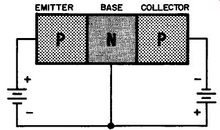
Fig. 307. Our forward-biasing technique remains the same, but note that
we have added another battery and that this battery forms a reverse-biased
connection between base and collector.
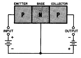
Fig. 308. We can break open the circuit of Fig. 307 for input and output,
as shown here.
And still more bias
Up to now we have been working with just one part of our transistor--the emitter-base circuit. We can add another battery, as shown in Fig. 307. This battery is connected between the collector and the base. But just how did we get our collector and base? The base is n-type germanium and the collector is p-type.
This, as we learned earlier, is one of the diodes we used to make our transistor. But note how this part of the transistor is biased.
The negative terminal of the battery is connected to the collector (p-type germanium) while the positive terminal goes to the base (n-type). What we have here is reverse biasing. And, just as in the case of the base-emitter circuit, we can vary the amount of reverse biasing by using a potentiometer, or by putting an ac voltage in series with the reverse-biasing battery.

Fig. 309. Here is the symbol for the p-n-p transistor. The symbol can
be put in any position and we can transpose the emitter and collector
leads for our convenience in circuit diagrams.
Input and output
With the help of Fig. 308 we can take another forward step.
The base-emitter circuit now has another name--input. And the base-collector circuit can also be identified in another way--out put. Fig. 308 is interesting in that it emphasizes the fact that the base is common to both input and output circuits. But, unlike the elements in a tube, separated by space, our three transistor elements, emitter, base and collector, are in very close contact.

Fig. 310. Formation of the p-n-p and n-p-n transistors follows the same
technique in both cases.
The transistor symbol
Just as a child in early school grades gradually puts away his blocks and takes to the use of more convenient numbers and letters, so too can we dispense with our block-diagram arrangement of the p-n-p transistor and use its electronic symbol. This is shown in Fig. 309. The base is marked with the letter B, the emitter with E, and the collector with C. The emitter and collector are always drawn at angles to the base. The emitter always has an arrowhead. For a p-n-p transistor, the first letter (p) al ways represents the emitter, the second letter (n) is the base and the third letter (p) is the collector.
The n-p-n transistor In constructing our transistor we started with a pair of p-n diodes. We joined the two n-sections and so the terminal point of this activity was a p-n-p transistor. But Fig. 310 shows that we selected just one of two possible ways of joining the diodes. We could have butted the two p-sections, and thus, as the illustration indicates, could have produced an n-p-n unit.
Biasing for the n-p-n transistor follows the same sort of arrangement we used for the p-n-p--that is, the input is forward-biased (as shown in Fig. 311) while the output is reverse-biased. Be careful, though. To make the n-p-n transistor, we transposed our pair of diodes, so now we must also transpose our bias batteries. Other than that, there is no difference between the two types of transistors.
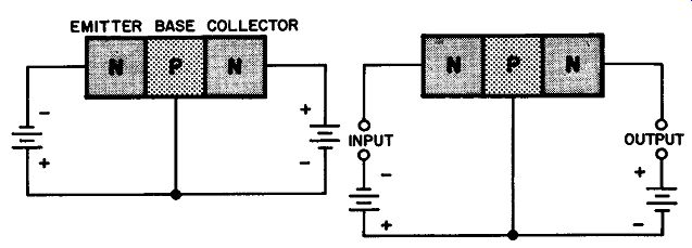
Fig. 311. The formation of the n-p-n circuit follows the same approach
we used for the p-n-p in Fig. 308.
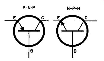
Fig. 312. Symbols for the p-n-p and n-p-n transistors. They are almost
identical. The only difference is in the emitter element.
For the p-n-p the arrow points inward to the transistor; for the n-p-n it points outward.
Electronic symbols
We have the electronic symbol for the n-p-n transistor in Fig. 312. We have also repeated the symbol for the p-n-p so that you can compare the two. The only difference is in the arrowhead.
In the p-n-p unit it points inward, while in the n-p-n it points outward.
No standard symbol has as yet been accepted for the transistor but, as you can see in Fig. 312, the differences are fairly slight.
Various letters are often used to represent transistors, but here, as in the case of symbols, there is no uniformity. The letter T (for transistor) is often used. (This is somewhat confusing since T is also used for transformer). An attempt has been made to popularize the letter Q, presumably because the letter does not represent any other component. In this guide we will use the. letter V (for valve) since the action of the transistor (like the tube) is valve-like in its behavior.
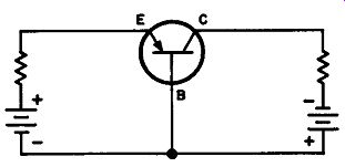
Fig. 313. With the addition of a few resistors, our elementary transistor
circuit begins to take shape.
Adding components
We now have our transistor, but, to add a few final touches to the picture, suppose we add a pair of resistors (as in Fig. 313). And so, with these few components, for both types of transistors (n-p-n and p-n-p) we are ready to learn how the transistor works and, having learned that, find out how we can put the transistor in key spots in a variety of jobs.
How the transistor works Up to now our block diagrams of the transistor created the impression that each of the blocks--emitter, base and collector-contained equal volumes of material. To have our two diodes work together as a transistor, let's modify our diodes and our thinking at the same time. We now want you to think of the base as an extremely thin section, compared to the emitter and the collector.
Continuing with our analysis of the transistor as an arrangement of diodes, look at Fig. 314. What we have here is a p-n-p transistor but we are using diode symbols. If we disconnect the lead going to the base, you can see quite readily that the two diodes and their biasing batteries form a series circuit. And since we have a series circuit, the current will be the same in all parts of the circuit. Also, take a good look at the batteries. They are connected in series aiding.
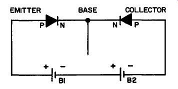
Fig. 314. The diodes and their biasing batteries form a series circuit.
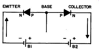
Fig. 315. This circuit is similar to that of Fig. 314 except that both
batteries and diodes have been transposed.
Just so that we won't be accused of showing a preference for the p-n-p type, we also have an n-p-n unit in Fig. 315. It is exactly the same as Fig. 314, except, of course, the diodes have been turned around, and so have the batteries. But the two diodes are still in series and the batteries still form a series-aiding pair.
What about current flow in the circuit of Fig. 315? Assuming current flow to mean electron flow, we can start at the negative terminal of BI. The current will move through the block of germanium marked n (the emitter), through the two combined (but very thin) p-regions (the base), into the n-region (the collector), and then from that region through B2 and B1 back to the starting point again.
Although we started this explanation by assuming that current first moved out of the negative terminal of B1, remember that this was just a matter of convenience. The current in a series circuit is a bit like a merry-go-round. Which part starts first? Unfair! Unfair! The circuits of Figs. 314 and 315 aren't really playing the game and we're violating some of our own rules. We've talked at great length about the diodes being forward- and reverse-biased, but the disconnected base lead in Fig. 315 isn't cricket. So, as shown in Fig. 316, let's connect the base lead to the junction of the two batteries.
Now you must admit that everything is quite proper. We have our two diodes--one forward-biased, the other reverse-biased.
What effect will this have on the current?
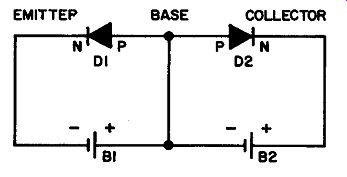
Fig. 316. With the connection of the base lead we provide a current
path be tween the base and battery B1.
Off-hand, you might argue that the two diodes could be represented by two resistors. Diode D1 in Fig. 316 is forward-biased, the current should be comparatively large, hence we could say it is equivalent to a small resistance. Diode D2 is reverse-biased, the current should be much smaller than through diode D1, hence its resistance is much higher. But D1 and D2 are in series. If we have a small resistor (say of I ohm) in series with one having a large value (say, 1,000 ohms) we can practically forget about the 1-ohm resistor as far as the total series resistance is concerned.
But D1 and D2 are not resistors. They're a pair of diode elements constructed in a very special way.
Since we cannot consider D1 as a low-value resistor only and D2 as a high value resistor only, let's see just how they do differ.
Let's analyze them from the viewpoint of an electron current. In Fig. 316, D1 is forward-biased. To trace the path of electron cur rent flow, suppose we start at the negative terminal of B1, since that is just as convenient a starting point as any. The electrons move along to the first diode, D1. Because this diode is forward biased, its potential barrier is pleasantly low, and so the electrons move easily enough into the base.
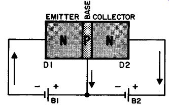
Fig. 317. Paths of current (electron) flow in the n-p-n transistor circuit.
Our electrons are now faced with the necessity for making a decision. They can either travel down the wire to the positive terminal of BI or they can make an effort to flow through D2 to the positive terminal of B2. Now everything we have told you up to now would make you think that there really is no choice. Going back to the plate of B1 we have a nice solid wire--an easy path for electrons. And, to clinch the argument in favor of such a path, D2 is reverse-biased and we know that it has a high potential barrier that opposes the passage of electrons. Yet, despite both of these factors, most of the electrons move through the second diode (D2) and from there through B2 and then back to battery B1. Since this is so contrary to the way the circuit would behave if we had a low-value resistor in place of D1 and a large resistor in place of D2, let's investigate a bit further.
We can do this by moving on to Fig. 317. We still have our two diodes, but now the base region is extremely thin. Furthermore, the base is common to both diodes. It is shared by D1 and D2.
As before, when the electrons get into the base region, they have a choice of going down the solid conductor to the positive terminal of B1 or, seemingly, struggling through the collector n-region.
To understand what is happening, let's go back to Fig. 315 for a moment. B1 and B2 are in series. The total voltage of these two batteries (because of the series connection) now exists between the n-type collector and the n-type emitter. And, as we saw way back in Section I, an electron likes nothing better than to move along the lines of force of an electric field. This is the same reason why electrons will move through a vacuum from a hot cathode (and sometimes a cold one) to a positive plate. As soon as the electrons find themselves in the base region, they feel the pull of the positive terminal of B1. But the voltage of B2 adds to the voltage of B1 to provide a strong electric field. So the potential barrier is overcome.
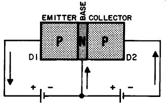
Fig. 318. Paths of current (electron) flow in the p-n-p transistor circuit.
However, the base is still a dividing point for the electron cur rent. Most of the current, though, proceeds through diode D2, with a much smaller amount flowing back to battery B1.
Our discussion of Fig. 317 centered around the n-p-n transistor.
What happens in the case of the p-n-p type? Exactly the same thing, except that the electron current flows in the opposite direction. Fig. 318 illustrates this. The arrows, representing the paths of electron flow, are opposite in Figs. 317 and 318.
Naming names
Not too long after the triode vacuum tube became popular, engineers found many reasons for giving the three elements added company. Grids were inserted, resulting in tetrodes, pentodes, and pentagrids. Probably the most widely-used receiving tube today is the pentode.
Like the tube, the transistor came into being as a three-element device. The transistor, though, is following its own evolution and since it is an entity in its own right, we have no reason for thinking that the transistor will follow the path trod earlier by the tube.
At this time, the most widely used transistor is a triode, although other types are available. The triode (tri, the prefix, means three) is a three-element device.
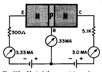
Fig. 319. Most of the current passes from the emitter to the collector.
The remainder flows from the base to the forward-biasing battery.
We have a name for each element in our transistor--emitter, base and collector. The word emitter would seem to indicate that electrons are boiled out, much as in the case of a hot cathode.
This isn't true, of course, since no heat is used. All we can say of the emitter (in the case of Fig. 317) is that it is electron-rich.
The collector (a good name) is so called (in Fig. 317) because it collects electrons. In a tube, the equivalent would be the plate.
We can consider the base in the manner of a control grid.
It would seem, in Fig. 318, that these names are now meaning less (except for the base) since the roles of collector and emitter are reversed. But this is only so because we have been considering current flow as electron flow. If, in Fig. 318, we think of the movement of holes, or positive charges, then the emitter is rich in positive charges and the collector is on the receiving end.
Amplification
In the circuit of Fig. 317 we managed to transfer most of the current flowing in a low-resistance circuit (the emitter-base circuit) to a much higher one. Thinking of this from a resistance viewpoint, we transferred (changed) a low-resistance circuit to a high-resistance one. But from transfer and resistor we manage to get transistor. Think of the transistor as being somewhat in the nature of a special type of step-up transformer. In this special transformer a variation of resistance in the primary will produce a variation of resistance in the secondary. It is this characteristic that enables us to use the transistor as- an amplifier and an oscillator. Let's see how we can go about getting amplification. We can do this by examining the circuit in Fig. 319.
In Fig. 319 we have an n-p-n transistor, a pair of bias batteries, a 300-ohm resistor in the emitter-base circuit (our input circuit) and a 5,100-ohm resistor in the collector-base circuit (our output circuit). Let us assume that we have a current of 3.33 ma beginning to flow. This current, in passing through the 300-ohm resistor, will produce a drop of almost 1 full volt across it. Most of the current (3 ma in this case) will pass through the base, over to the collector. A small amount of current (.33 ma) will go through the base to the input bias battery.
We now have 3 ma of collector current flowing through our 5,100-ohm collector resistor. This will result in a drop of 15.3 volts across it.
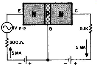
Fig. 320. A signal voltage (represented by the symbol for an ac generator)
varies the amount of forward biasing, thus varying the current flowing
to the collector.
So far we have nothing that could be called spectacular. The two resistors, plus the transistor, are acting as a de voltage divider across the two series batteries. But suppose, as in Fig. 320, we put an ac signal source in series with the emitter-base input. This ac source is going to supply an emf that is 1 volt peak-to-peak.
At its maximum negative peak point, the ac voltage will add one half volt to the input battery voltage. At its maximum positive peak, it will subtract one-half volt. Consider what happens when one-half volt is added. Our forward-biased section becomes even more so. Since we have added a voltage in series aiding with our other batteries, more current will flow. In Fig. 320 the current will rise to 5 ma.
To make our arithmetic a bit easier, imagine that all of this current will go over to the collector. With 5 ma flowing through the 5, 100-ohm resistor, the drop across it will now become 25.5 volts. But since we had 15.3 volts to begin with, we have an in crease of 10.2 volts in our output circuit. What about the input?
In the ratio of 10.2 to 0.5, or 20.4 to 1.
When the signal voltage changes, it will be in opposition to the battery voltage. This will decrease the forward bias (or in crease the input resistance), lowering the current. If we get a proportionate decrease in current, the ratio of output voltage to input voltage will still be 20.4 to 1.
We could have obtained exactly the same results by using a p-n-p transistor instead of the n-p-n we used in Fig. 319. The batteries would be transposed. And while the voltage drops across the input and output resistors would still show us a ratio of 20.4 to 1, the polarities of these voltage drops would be exactly opposite to those of the n-p-n circuit.
We know you are going to agree that the n-p-n circuit of Fig. 320 can immediately be classified as a rather simple type. It certainly has few enough components! However, Fig. 320 is a sort of hybrid diagram, since we are using circuit .elements for the components and a block-diagram style for the transistor. All we need do now is take just one small step forward, use the symbol we learned earlier for the transistor, and end up with a complete schematic as shown in Fig. 321. This diagram, of course, represents the same action we got in Fig. 320. Current amplification--alpha If, for some reason, we did not have the services of the forward biased portion of the transistor (it could be shorted), collector current would be a function of the emitter-collector bias battery.
Because of the reverse-biasing action, collector current would be very low indeed. However, if we allow our forward-biasing section to work properly, collector current rises considerably. In this sense, then, the transistor is a current-operated device.
Not all the electrons that enter the emitter make the full transit through the transistor. Percentage-wise, somewhere between 95 and 99 percent do manage to make the complete trip, but a few percent do get sidetracked through the base, back to the forward biasing battery. If we manage to increase the emitter current (as we did before) the collector current will also increase (but not to the same extent). This ratio between a change in collector cur rent and a change in emitter current is known as the current amplification factor. The Greek letter alpha (a) is used to indicate this characteristic of the transistor.
It may seem very strange that we talk about current amplification, especially since collector current is invariably lower than emitter current, but remember how this extraordinary situation came about. If it were not for the forward-biased emitter-base circuit, the current in the collector-base circuit would be a very small fraction of the current. Since alpha is less than unity, we generally discuss it in terms of percentage. Typical values of alpha are 95 to 99%.
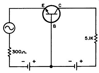
Fig. 321. Elementary transistor amplifier circuit.
Current amplification--beta
When we change the amount of emitter current, not only does the collector current change, but the base current as well. The ratio of the change in collector current to the change in base cur rent can also be used as a measure of the amplification of the transistor. It is represented by the Greek letter beta (β). Since collector current is so much larger than base current, beta is in terms of whole numbers. Thus the beta of a transistor might be 20, or 30 or 40, etc. A transistor with a beta of 40 means that 40 times more current flows in the collector than in the base circuit.
Quite naturally, the more current we have in our collector circuit the more current will flow through the resistor connected to the collector and the greater will be the voltage drop across it.
Since our output is taken from across this resistor, we naturally want as much current through it as we can get. This means, in terms of alpha, that we would like to have alpha as high a percentage as possible--that is, as close to 100 percent as we can get. In terms of beta, we would want the number to be as large as possible. A transistor with a beta of 100 has more amplification than a transistor with a beta of only 20.
Alpha and beta
Obviously, we cannot change alpha without affecting beta. The relationship between the two can be put into a very simple formula so that we can calculate the value of alpha (if we know beta) or the value of beta (if we know alpha). This is the formula:
beta = alpha/ 1 - alpha
We can make our work much easier if we use letters:
/3 = a/ I--a Example 1: A transistor has an alpha of 95%. What is the value of beta?
/3 = a/ I--a since 95% is the same as .95
/3 = .95/1--.95
/3 = .95/.05 = 19 Example 2: A transistor has a beta of 45. What is the value of alpha?
/3 = a/I--a 45 = a/l--a
If we multiply both sides of this equation by 1--a we will get: 45(1--a) = a 45--45a = a
We can now transpose the -45a to the right-hand side: 45 = 45a + a or 45 = 46a
Dividing both sides of the equation by 46, we get: 45/46 = a or a= .978 or 97.8%
Voltage amplification
Ultimately, in dealing with an amplifier such as the transistor, we must come back to the idea of voltage amplification. We start with a signal voltage and this signal voltage changes the current flowing through the transistor. But this flow of current must be translated into a form we can use. In passing through the output resistor, the resistor connected in series between the collector and its bias battery, we get a voltage. To the extent that this varying voltage is greater than the signal voltage, we get amplification.
The waveform of the voltage across the output resistor should be the same as that across the input resistor since the change in cur rent is being produced by the input voltage. The technique is just the same as that used by a vacuum tube amplifier where the signal voltage, inserted between grid and cathode, modifies the tube's bias. It might seem strange to talk about voltage amplification since the collector current is less than the emitter current, even though by just a small amount. It is the great difference be tween the output or load resistance and the input resistance that helps produce voltage gain. The difference between emitter and collector current might be small, but there is a deliberately large difference between input and output resistances.
The transistor as an oscillator
Basically, an oscillator is a de to ac converter. We take the voltage and current supplied by the battery (or batteries) and change this de voltage and current (with the help of the oscillator) into ac form. The most commonly used technique is to take some of the energy of the output circuit and feed it back, in phase, to the input. But before you decide that what we have here is a perpetual motion machine, remember that the energy is supplied by the battery, and that the ac power we get out of the oscillator is never quite as much as the de power we put in. In oscillators, as in so many other things, you get nothing for nothing.
Fig. 322 shows a simple oscillator arrangement. Oscillator circuits will be covered in greater detail in Section 6. What we have in Fig. 322 is a stripped-down version for purposes of explanation.
The only change of interest is the addition of the transformer which couples the output (collector) circuit back to the input (emitter). If you will trace the path of current flow, you will see that each transformer winding is in series with the transistor and the bias batteries.
Fig. 322. Elementary transistor oscillator circuit.
The feedback winding, F, has very few turns. The resistance of the winding is very low and so its ohmic resistance has very little effect on the current. The winding soldered to the collector lead has many more turns. And while the current flowing through that winding is de, yet the moment the circuit is closed, there is a rapidly growing magnetic field around the winding. A voltage is induced across winding F. But this voltage is in series with the emitter-base biasing voltage. If the induced voltage is phased so that it adds to the forward bias, the flow of current to the emitter will be increased. This increased current (most of it) will also flow through the collector and the collector winding. The growing magnetic field around the collector winding induces more voltage across winding F, which, in turn causes more current to flow.
But all good things must come to an end. The induced voltage across F depends on the rate of change of the magnetic flux. The combination of induced voltage plus battery bias is no guarantee that the current will continue to increase indefinitely. The current gradually slopes off and approaches a steady state value. All this means is that the current keeps increasing, but more and more slowly.
However, the change in the magnetic field around the collector winding depends on how rapidly the current through it changes.
If ·the rate of current increase diminishes, so will the variation of the magnetic field around the collector winding. But this means less voltage will be induced across winding F. Less voltage, across F, though, means a smaller amount of current going to the emitter.
We now have a condition of a decreasing current through the collector winding. As a consequence, the polarity of the induced voltage changes, and now, the induced voltage, instead of aiding the forward bias battery, opposes it. With this sort of situation, the current rapidly drops to almost zero. This means that the magnetic field around the transformer is also so small as to be in effectual. The forward bias battery now takes over again, because the opposition voltage across winding F has disappeared. This is where we came in, since the entire cycle of events repeats itself.
We have taken some liberties with this description of oscillator action since certain important components were omitted and since we have had no discussion as yet of transistor current curves. The description is of use since the behavior of a transistor as an oscillator is similar to that of its vacuum tube counterpart.
Transistor manufacture
You will note that at no point in these first three sections have we supplied any information on how transistors are manufactured.
This is a highly specialized technique and there would be no point to our engaging in such discussion. However, there are numerous transistor types--so many that they deserve a section all to themselves. But even in the section on transistors (other than the triode) it would be impossible to describe all the new ones. Not only is there a large and growing variety, but developments now include semiconductors that behave somewhat like transistors, but which cannot be named as such. Fortunately, the basic theory presented earlier will help you reach a more ready understanding of the way in which they work.
So we come to the end of another section. We know you may be impatient to come to grips with practical circuits, but our introduction to the transistor has barely been completed. Before we concern ourselves with circuitry, we need to know more about the transistor, its special characteristics, its likes and dislikes, and its needs and its efficiency.
QUIZ
1. What is beta?
2. What is alpha?
3. A transistor has a beta of 65. What is the value of alpha?
4. A transistor has an alpha of 98%. What is the value of beta?
5. How do the values of emitter, base and collector currents compare?
6. How is the emitter-base circuit biased? The collector-base circuit?
7. How does the volume of the base compare with that of the emitter or collector?
8. What is the technique used for varying the forward bias of a transistor?
9. How was the word transistor obtained?
10. What is the difference between high impedance and low impedance?
11. What is the difference between impedance and resistance?
12. What is reactance? What is the difference between reactance and resistance?
13. In a p-n-p transistor, which element is represented by the letter p? Which by the letter n? And which by the final letter p?
14. What is the difference in electron current flow in a p-n-p transistor compared to an n-p-n type?
15. How does the input impedance of a transistor compare to the output impedance?