AMAZON multi-meters discounts AMAZON oscilloscope discounts
Separate descriptions of the other types of components likely to be met in electronic circuits are given in this section for ease of reference. Many are variations on standard components previously described, but with different working characteristics. The diode family, for example, is particularly numerous.
THE DIODE FAMILY
Diodes are used in a wide variety of applications. See Section 9 for information on general purpose diodes.
Zener Diodes
The Zener diode is a special type of silicon junction diode which has the particular characteristic that, when reversed bias voltage is applied and increased, there comes a point where the diode suddenly acts as a conductor rather than an insulator. The point at which this occurs is called the breakdown voltage (or Zener point), which, once reached, remains constant, even if the negative bias voltage is increased. In other words, once negatively biased to, or beyond, the breakdown voltage, the voltage drop across the diode remains constant at its breakdown voltage value, regardless of the actual current flowing through the diode.
This important characteristic makes Zener diodes particularly useful as a source of constant dc voltage, or stabilizing a supply voltage, using the type of connection shown in Fig. 11-1. A series resistor (R) is necessary to limit the amount of current flowing through the diode, otherwise it could be burned out. Regardless of the value of the input volts, the voltage dropped across the Zener diode will remain constant, so any variations in the input voltage will not affect the output voltage tapped from across the Zener diode. This voltage will be the breakdown voltage of the diode, which may range from about 2.7 volts up to 100 volts or more, depending on the construction of the Zener diode. If the input voltage falls below the break down voltage, of course, the Zener diode will stop conducting and break the circuit.
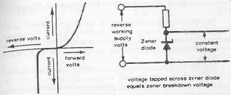
Fig. 11-1. A Zener diode, working with reverse bias, breaks down at a specific
reverse voltage. Connected as shown, it can be used as a source of constant
voltage supply. Note the symbol for a Zener diode.
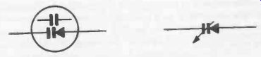
Fig. 11-2. Alternative symbols for a Varicap.
Performance of a Zener diode as a voltage-stabilizing device is limited only by the power rating, which may be quite low-under 500 mW for the small Zener diodes, but up to 5 watts or more in larger sizes. Its stability will also be affected by the heating effect of the actual current flowing through it, causing a shift in the breakdown voltage, so the nominally constant voltage can vary with working temperature.
If this is likely to be troublesome (the type of Zener diode used has a fairly high temperature coefficient of resistance), then connecting two similar diodes in series can greatly improve the temperature coefficient. Also, the power rating will be increased.
Varicap Diodes
Another special type of diode is the Varicap or varactor. These behave as capacitors with a high Q (see Section 6) when biased in the reverse direction, the actual capacitance value being dependent on the bias voltage applied. Typical applications are the automatic control of tuned circuits, "electronic tuning," adjusting capacity in the circuit, and thus resonant frequency, in response to changes in signal voltage; automatic frequency control of local oscillator circuits in superhets and TV circuits; and also as frequency doublers and multipliers. Symbols for a Varicap are shown in Fig. 11-2.
The tunnel diode is another type with special characteristics, unlike that of any other semiconductor device. It is constructed like an ordinary diode but the crystal is more heavily doped, resulting in an extremely thin barrier (potential layer). As a consequence, electrons can tunnel through this barrier.
This makes the tunnel diode a good conductor with both forward and reverse voltage. Behavior, however, is quite extraordinary when the for ward voltage is increased, see Fig. 11-3. Forward current at first rises with increasing forward voltage until it reaches a peak value. With increasing forward voltage, current then drops, to reach a minimum, or valley, value.
After that it rises again with further increase in forward voltage. Worked the region from peak voltage to valley voltage, the tunnel diode negative resistance characteristics. Another interesting feature is that any forward current value between peak and valley value is obtainable three times (at three different forward voltages).
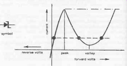
Fig. 11-3. Symbols (left) and characteristic performance of a tunnel diode.
From "peak" to "valley" it exhibits negative resistance.
Tunnel diodes have a particular application for very high speed switching, with a particular application to pulse and digital circuitry, e.g., digital computers.
Schottky Diode
The Schottky diode is a metal semiconductor diode, formed by integrated circuit techniques and generally incorporated in ICs as a "clamp" between base and emitter of a transistor to prevent saturation. Voltage drop across such a diode is less than that of a conventional semiconductor diode for the same forward current. Otherwise, its characteristics are similar to that of a germanium diode. A typical circuit employing a Schottky diode is shown in Fig. 11-4.
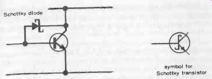
Fig. 11-4. Typical circuit for a Schottky diode (left) and the equivalent
single component, a Schottky transistor (right). symbol for Schottky transistor.
For such circuits (i.e., using a Schottky diode as a clamping device associated with a transistor) diode and transistor may be produced at the same time in processing the transistor. This combination device is called a Schottky transistor (see also Fig. 11-4).
Photodiodes
It is a general characteristic of semiconductor diodes that if they are reversed biased and the junction is illuminated, the reverse current flow will vary in proportion to the amount of light. This effect is utilized in the photodiode which has a clear window through which light can fall on one side of the crystal and across the junction of the P- and N -zones.
In effect, such a diode will work in a circuit as a variable resistance, the amount of resistance offered by the diode being dependent on the amount of light falling on the diode. In the dark, the photodiode will have normal reverse working characteristics, i.e., provide almost infinitely high resistance with no current flow.
At increasing levels of illumination, resistance will become proportionately reduced, thus allowing increasing current to flow through the diode. The actual amount of current is proportionate to the illumination only, provided there is sufficient reverse voltage.
In other words, once past the "knee" of the curve (Fig. 11-5), the diode current at any level of illumination will not increase substantially with increasing reverse voltage.
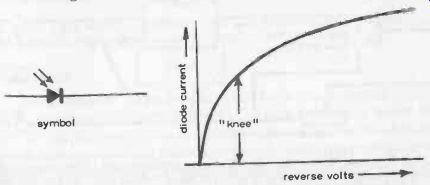
Fig. 11-5. Symbol (left); and characteristic performance of a photodiode.
Photodiodes are extremely useful for working as light-operated switches, a simple circuit being shown in Fig. 11-6. They have a fairly high switching speed, so they can also be used as counters, counting each,, interruption of a beam of light as a pulse of current.
There are two other types of light-sensitive diodes--the photovoltaic diode and the light emitting diode (or LED). The photovoltaic diode generates voltage when illuminated by light, the resulting current produced in an associated circuit being proportional to the intensity of the light. This property is utilized in the construction of light meters. The amount of current produced by a photodiode can be very small, and so some amplification of the current may be introduced in such a circuit. Special types of photodiodes are known as photocells and are generally more suitable for use as practical light meters.
The light-emitting diode works the opposite way round to a photodiode.
emitting light when a current is passed through it. Light-emitting diodes are described in Section 10.
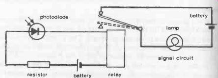
Fig.
11-6. Photodiode used as a "light" switch. The rise in current
when the diode is illuminated makes the relay pull in completing an external
circuit through the'; relay contacts.
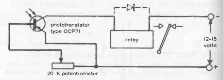
Fig. 11-7. Practical "light switch" circuit using a phototransistor.
The relay should be of sensitive type and adjusted to pull in at about 2 milliamps.
The potentiometer is a sensitivity control. A diode connected across the relay
will improve the working of this circuit.
THE PHOTOTRANSISTOR
The phototransistor is much more sensitive than the photodiode to, changes in level of illumination, thus making a better "switching" device where fairly small changes in level of illumination are present and must be detected. It works both as a photoconductive device and an amplifier of the current generated by incident light. A simple circuit employing a photo-transistor is shown in Fig. 11-7.
A phototransistor and a light -emitting diode (see Section 10) may be combined in a single envelope, such a device being known as an opto isolator. In this case, the LED provides the source of illumination to which the phototransistor reacts. It can be used in two working modes-either as a photodiode (Fig. 11-8) with the emitter of the transistor part left disconnected, or as a phototransistor, see Fig. 11-9. In both cases, working is governed by the current flowing through the LED section.
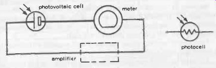
Fig. 11-8. Basic photovoltaic diode circuit (note symbol for photovoltaic
diode). Shown on right is symbol for a photocell. photovoltaic cell photocell
amplifier.
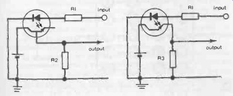
Fig. 11-9. Opto-isolator (combined LED and phototransistor), working as a
photodiode (left); and phototransistor (right).
SOLAR CELLS
The photodiode is a photovoltaic cell. That is to say, light falling on its Junction produces a voltage. This voltage measured on open circuit (e.g., with a very-high -resistance voltmeter connected across the cell), is known as the photovoltaic potential of the cell. In this respect it is like a dry battery. Connected to an external load, the cell voltage will fall to some lower value dependent on the resistance in the circuit (see Section 18).
Photovoltaic cells will develop a potential when illuminated by any source of light. The photovoltaic potential will depend on the construction of the cell, but for any given cell, will be proportional to the intensity of the light.
The solar cell is a photovoltaic cell (silicon photodiode) to respond to sunlight. Typically, it is a small wafer about V4 in. (6. 5inn) square, coated with varnish to protect the junction. In average sunlight (about 3,000 lumens per sq. ft.), its photovoltaic potential is of the order of 500 mV. Connected to a 100 -ohm load, it will generate an output current about 3 mA.
To get higher voltages and currents from a solar battery, a number o cells have to be used connected in series -parallel. Series connection gives cell voltage equal to the sum of the individual cell voltages. Parallel connection gives a current equal to the sum of the individual cell currents.
Suppose, for example, the solar battery was intended to operate a circuit requiring a nominal 2 volts and give a current of 15 milliamps through a 100 ohm load. From the voltage consideration, number of cells 2 divided by 500 mV ( voltage per cell) = 4 cells.
From current considerations, number of cells required =15 divided by 3 (current per cell) = 15 cells.
The solar battery required would thus have to consist of five rows each of four cells, each row consisting of four cells connected in series, and each row being connected together in parallel, Fig. 11-10.
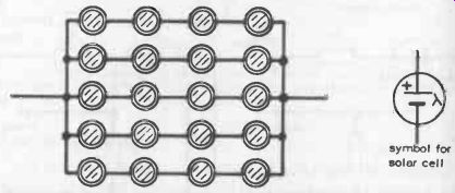
Fig. 11-10. Connections for a 2-volt solar battery to give a current of 15
milliamps through a 100 ohm load.
A single solar cell can be used to measure solar power, or rather the strength of sunlight at any time. The cell is simply mounted on a suitable panel, sensitive side (negative side) facing outwards, and the two cell leads connected to a 0-10 milliammeter, Fig. 11-11A. Directed towards the sun, the meter will then give a reading representative of the strength of the sunlight. To measure maximum or peak radiation, point the cell directly towards the sun. To use the instrument as a device for plotting solar energy, called a radiometer, the panel should be pointed due south and tilted upwards at an angle approximately 10 degrees more than the local latitude.
Readings are then taken at intervals throughout the day, indicating how , much solar energy the panel is receiving.
If the meter readings are very low, add a shunt resistor across the meter (shown in broken lines) in Fig. 11-11B.
This needs to be a very low value (1 or 2 ohms only). Find a suitable value by trial and error to give near maximum meter reading in the brightest summer sunlight.
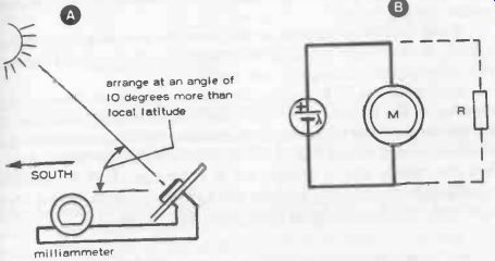
Fig. 11-11. Aligning a photocell to measure solar energy (left).
The circuit on the right is a complete solar energy meter, the meter used being a 0-50 milliamp type.
RECTIFIERS
The conventional diode is a rectifier, its maximum forward current capabilities being determined mainly by its junction area. For signal rectification, point contact diodes are usually preferred (see Section 9), which may limit maximum forward current to 30 to 50 mA, depending on type.
Where higher powers are required, larger rectifier diodes can be used, with maximum current ratings up to several amps.
In the case of power supplies (see Section 26), four diodes in bridge configuration are normally used for full-wave rectification. Physically, this does not mean that four separate diodes have to be connected up, see Fig. 8-5. Bridge rectifiers are available as integral units. The average voltage output from such a bridge is 0.9 times the root-mean-square voltage developed across the secondary of the transformer, less the voltage drop across the rectifier itself.
Metal plate rectifiers are still used for high-voltage applications. Each plate is essentially a diode, with a number of plates stacked in series or series-parallel to accommodate the voltage and power loading required.
Exactly the same principle can be extended to semiconductor diodes.
Selenium rectifiers, which were originally widely used for voltages up to about 100 rms have now been virtually replaced by silicon diodes.
Silicon controlled rectifiers or SCRs (also known as thyristors) are silicon diodes with an additional electrode called a gate.
If a bias voltage is applied to the gate to keep it at or near the same potential as the cathode of the diode, the thyristor behaves as if working with reverse voltage with both directions of applied voltage, so only a small leakage current will flow, fr. If the gate is biased to be more positive than the cathode, the thyristor behaves as a normal diode. In other words, the gate can be used to turn the rectifier on (by positive bias on the gate), thus enabling forward current to be controlled (e.g., preventing forward current flowing over any required; portion of a half cycle).
A triac is a further variation on this principle, providing bidirectional , control. It is virtually a double -ended thyristor which can be triggered with either positive or negative gate pulses.
Structurally, an SCR is a four-layer diode, with connections to the inner layers. The terminal connected to the P-region nearest the cathode is the cathode gate, and the terminal connected to the N -region nearest the anode the anode gate, see Fig. 11-12. Both gates are brought out in a triac.
Only the cathode gate is brought out in a thyristor. Both devices are essentially ac switches, the thyristor being effective only on one half of an ac voltage, and the triac being effective on both halves.
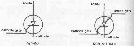
Fig. 11-12. Symbols for thyristor and SCR.
THERMISTORS AND SENSISTORS
A thermistor is a device designed specifically to exploit the characteristic of many semiconductor materials to show marked reduction in resistance with increasing temperature. This is the opposite effect exhibited by most metal conductors where resistance increases with increasing temperature.
The obvious value of a thermistor is to "balance" the effect of changes in temperature on component characteristics in a particular circuit, i.e., work as a compensating device by automatic adjustment of its resistance, down (or up), as working temperatures rise or fall and resistances of other components rise or fall. Compensation for temperature changes of as much as 100° C are possible with thermistors- a typical application being shown in Fig. 11-13. Here, the thermistor is used to stabilize the working values of the resistors in an audio amplifier circuit.
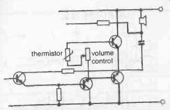
Fig. 11-13. Practical circuit incorporating a thermistor to counteract fluctuations
in value of other resistors in the circuit due to heating effects or temperature
changes.
Another use for a thermistor is to eliminate current surges when a circuit is switched on "from cold." Certain circuits may tend to offer relatively low resistance when first switched on, which could produce a damaging surge of high current.
A thermistor in the supply line with a relatively high "cold" resistance limits the initial peak current surge, its resistance value then dropping appreciably as it warms up so that the voltage dropped across the thermistor under normal working conditions is negligible.
Thermistors are made in the form of rods, looking rather like a carbon rod, sintered from mixtures of metallic oxides. They are not made from the usual semiconductor materials (germanium and silicon) since the characteristics of a thermistor made from these materials would be too sensitive to impurities.
Sensistors are similar devices working in the reverse mode, i.e., their resistance increases with temperature, and vice versa. They thus behave like metallic conductors, although they are made from heavily doped semiconductor material.