AMAZON multi-meters discounts AMAZON oscilloscope discounts
A circuit diagram is a plan of a particular circuit showing all the components and all the circuit connections. The components are represented by symbols (see Section 1), arranged to show all connections simply and clearly, avoiding crossing lines as far as possible.
It is a theoretical diagram since it does not show the actual size or shape of components, nor their actual position in a built-up circuit. So it has to be redrawn as a practical diagram or working plan from which the circuit is actually constructed.
Certain conventions apply in drawing a (theoretical) circuit diagram, but these are not always followed rigidly. The first is that the diagram should read from left to right.
That means whatever is input to the circuit should start at the extreme left and be fed through the circuit from left to right. Thus in the simple radio circuit shown in block form in Fig. 19-1 the input is supplied by the aerial current feeding the tuned circuit, then passing to the detector, then to the amplifier and finally the loudspeaker output.
The power supply for the circuit (say a battery) is shown on the far right of the circuit. At first this may seem a contradiction of the rule, if one thinks of the power supply being put into the circuit. But it is not a true input; merely a supply to work the circuit, and otherwise nothing to do with the circuit.
So it is depicted out of the way on the right. There is another good reason for this. Although the supply will feed all the stages backwards in terms of left-to-right reading, it probably will not be required to power the first stage. Hence, it is logical to show feed from the right, stopping at the appropriate stage.
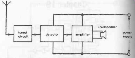
Fig. 19-1. Basic stages in a simple radio receiver.
Nearly all circuits are based on a common line connection, i.e., components in various stages are connected to one side of the supply. This common line is drawn at the bottom of the diagram, as shown in Fig. 19-2, is generally referred to as the common ground line, although it may not have any actual connection to ground.
A similar common line can also be drawn at the top of the diagram, representing the other side of the supply. Conventionally, this top line is the +, and the bottom or common line the -. This is not always convenient in designing transistor circuits, so this conventional polarity may be re versed on some diagrams.
Working on this basis, and replacing the boxes with individual components, the circuit diagram then looks something like Fig. 19-3. Each component is identified by a number, or may have its actual value given alongside. Reading the circuit is fairly straightforward-with a little practice. Starting from the left, the input from the aerial is fed to L and C1 forming the tuned circuit. From there, it is passed through the diode detector to the amplifier (TR1). TR1 then feeds the final output stage (transistor TR2) driving the loudspeaker. A supply voltage is required only by TR1 and TR2, so the upper common line stops short at TR1 stage. The resistors in the top half regulate the supply; and those in the bottom half (connecting to the common bottom line) establish the working point of the transistors. Additional components (C2 and C3) are required for coupling between stages.
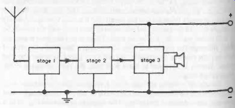
Fig. 19-2. Stages shown with "common ground" and power supply connections.
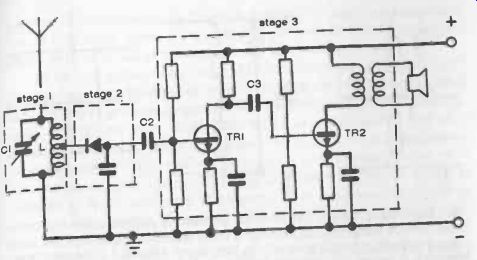
Fig. 19-3. The same stages drawn with all components and all connections required.
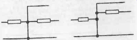
Fig. 19-4
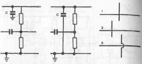
Fig. 19-5. The capacitor (C) is connected between top and bottom lines, but
may be shown in a circuit diagram in either of these two ways. On the right
are three ways of drawing crossing lines with no connection. Method 1 is the
usual way.
Method 2 is clearer; and method 3 clearer still.
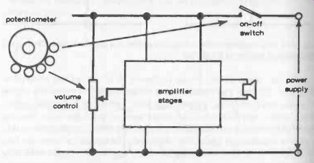
Fig. 19-6. In this example, a single component (the potentiometer connections)
appears in two separate parts of the circuit diagram.
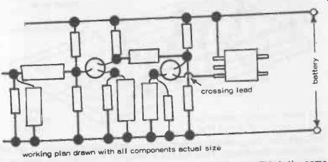
Fig. 19-7. Typical component layout drawing or working plan. This is the same
circuit as Fig. 19-3, following the tuned circuit (which would be a ferrite
rod aerial).
Note that all connecting lines meet at right angles, and where such connection occurs, this is further made clear by a .
If a line on the diagram has to cross another line without any connection to this line, it is simply drawn as a crossing line, as shown in Fig. 19-5 (right).
Crossing lines with a at the point of meeting indicates that all four lines are, in fact, connected at that point. To avoid possible confusion (or accidentally missing out the .), connected lines from each side of another line can be drawn as shown in the right hand diagram of Fig. 19-4.
Fig. 19-4. Two methods of indicating connection to a common point. That on
the right is often preferred for clarity.
So far, there should be no confusion at all in reading theoretical diagrams, but they can become more difficult to follow when the circuit becomes more complex or contains a large number of individual components. One common trick-of -the -trade used to avoid too many crossing lines (which could lead to mistakes in following a particular connection) is to arrow a connecting point, or separately designate a common line connection-Fig. 19-5. Arrowing is usually applied to outputs, indicating that this line is connected as an input to a separate stage (or even a separate circuit). Showing a separate ground connection is common with components connected between the top line and bottom line. It indicates clearly that the component is to be connected to the ground line, and avoids having to draw this line in close proximity to other components or crossing other lines.
What is less easy to read in terms of actual connections is a circuit incorporating a single physical component which may perform two (or more) separate functions. As a very simple example, a volume control potentiometer for a radio may also incorporate on -off switching. The two functional features of this single component may appear in quite separated parts of the circuit, e.g., the volume control prior to an amplifier stage and the switch function in the supply line at the far right -Fig. 19-6.
This can be even more confusing at first where a ganged tuning capacitor, or a ganged switch is involved, its separate sections appearing in different parts of the circuit, although it is actually a single physical component. This is the logical--and by far the simplest--way of showing the theoretical connections of the circuit, but when it comes to actual construction of the circuit, connections from two or more different parts of the circuit have to be taken to one particular component position.
As far as possible, actual physical layout of components should follow the same flow path positions as in the theoretical circuit diagram, adjusted as necessary to get components into suitable positions for making connections. Exceptions must arise, particularly as noted above. Just as a theoretical diagram is designed to present the circuit in as simple a manner as possible with all theoretical connections clear, the working circuit must also be planned to be as neat and simple as possible and also as logical as possible as far as placement of components is concerned. It should be prepared as a complete wiring diagram, when it becomes a working plan.
Almost inevitably, it will look more confused than the theoretical diagram, with probably a fair number of crossing wires (unless planned as a printed circuit-see Section 21) and leads running in various directions. Common connecting points are still indicated by a , but crossing leads are better shown as definite crossovers, as in Fig. 19-7.
Then there is less risk of wondering whether or not a has been missed at that point in preparing the working diagram, particularly as it will be less easy to check connections on a working diagram than on a theoretical circuit diagram.
The theoretical circuit diagram, however, remains the check reference for the working plan-and for checking the circuit when built. It may also be the only guide available for establishing the correct way to connect a diode or a polarized capacitor (electrolytic capacitor).
Following the direction of current flow (and thus the polarity at any particular point), should be fairly straightforward, remembering that with a + top line, the direction of current flow will be downwards (from top line to bottom line), through various components on such paths.
If the top line is - , the flow direction is obviously reversed.
It is also easy to check the direction of current flow through transistors by the arrow on the emitter in the transistor symbol.
Direction of current flow out of the transistor via the collector will follow in the same direction. Direction of current flow into the base of the transistor will be opposite to that of the emitter arrow direction. Figure 19-8 should make this clear.
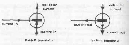
Fig. 19-8. Direction of current flow through PNP and NPN transistors.
These rules for reading the current flow through transistors should also make it fairly simple to determine the current flow with horizontally connected components on the circuit diagram, and thus establish the correct polarity for electrolytic capacitors appearing in these lines.