In the previous SECTION vectors and vector ideas were used in the solutions of various types of networks involving resistance, inductance, and capacitance. But vectors can be used in many other applications, either as a tool for calculations, or in analyzing circuit operation for many different types of circuits.
A conventional amplifier shifts the phase of an input signal by 180° between grid and plate. Oscillators must have in-phase feedback to sustain oscillations. High-quality audio amplifiers use degenerative feedback (180° out of phase) to improve the frequency response. Then, on the other hand, receivers in two way radio systems may use regenerative (in-phase) feedback to reinforce the signal and thus increase audio output. There are many other examples in which degenerative or regenerative actions play a part in circuit operation.
In-between angles also enter into electricity and electronics to a large degree. Some circuits use phase as an analog type of information, representing some particular quantity. Frequency modulation and demodulation are examples; changes of frequency or phase represent changes of audio amplitude. This SECTION explains several different electrical and electronic circuits or systems in which phase plays an important part in the operation. The choice of circuits follows no particular pattern ; those described were chosen simply because they are relatively simple analyses involving phase. The idea here is not so much to teach circuitry and operation, but to illustrate how vectors and phase can be used to secure a better understanding of circuit operation.
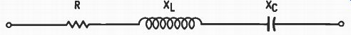
Fig. 6-1. An LCR series circuit.
RESONANCE
The LCR circuits solved previously used more or less random values of circuit parameters. Resonance, however, is a special condition of an LCR circuit, such as that in Fig. 6-1. Such a series circuit is resonant at the frequency at which inductive and capacitive reactances are equal. The resonant frequency formula,
f = 1 2 pi LC has been derived from that relationship of reactances.
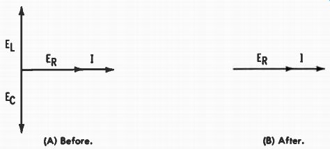
Fig. 6-2. Voltage and current vectors of Fig. 6-1 before and after vector
addition. (A) Before. (B) After.
Currents through all the components of a series circuit are the same so that with equal reactances the voltage drop across the inductance equals the voltage drop across the capacitance.
This is shown in Fig. 6-2A, in which circuit current is used as reference. The voltage across the resistance is in phase with the current, the inductive voltage leads the current by 90°, and the capacitive voltage lags current by 90°. A vector addition of the reactive voltages shows that they effectively cancel each other, leaving a vector resultant as shown in Fig. 6-2B. The circuit at resonance is purely resistive, and as the reactances cancel the effects of each other, the only effective circuit opposition is the resistance. So impedance is minimum and current is maximum in the series LCR circuit when operated at its resonant frequency.
The ideal parallel resonant circuit would include no resistance at all, only a perfect capacitor connected in parallel with a perfect inductor across an AC source. In such a circuit the capacitive current leads the applied voltage by 90°, as shown in Fig. 6-3A. The inductive current lags the applied voltage by 90°. As the currents are equal and opposite, the total circuit current is zero (Fig. 6-3B), meaning that the parallel LC circuit represents an infinite impedance at the resonant frequency.
IC IL E E
(A) I c and I L are equal and opposite. (B) l e and I L cancel, leaving only E.
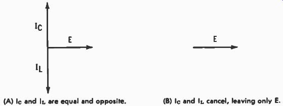
Fig. 6-3. Vectors of an ideal parallel r t circuit.
However, a practical parallel LC circuit includes resistance, most of which is in the inductive branch and which consists primarily of the resistance of the coil. Assuming a small amount of resistance in the inductive branch and zero resistance in the capacitive branch, a vector representation is shown in Fig. 6-4. As in any parallel circuit, the same voltage appears across both branches, and it is labeled E. as in Fig. 6-4.
Current through the capacitor (L) leads the applied voltage by 90°. Current through the inductive branch (including L and R) lags the applied voltage by something less than 90° and is labeled I L. Voltage EL leads the current through it by 90° and leads the applied voltage by a smaller angle.
The voltage across the resistance ( ER) is in phase with current I L, bearing in mind that the same current flows through It and L. Adding EL and ER at 90° gives the applied voltage E., shown as the diagonal of the parallelogram. This part of the analogy would hold for the series RL branch regardless of whether or not the capacitor were connected in parallel. The total circuit current cannot be zero because the currents in the two branches are not equal. Total current ( I T) is the diagonal of the parallelogram that includes L and I L as adjacent sides.
This arrangement acts resistively because total current is in phase with the applied voltage, but the total is smaller than that through either of the separate branches.
From this analogy it is seen that true parallel resonance does not occur at the frequency at which the reactances are equal.
For true resonance the inductive current must be larger than the capacitive current by an amount that causes I, to be in phase with the applied voltage. In order to have this condition occur the inductive reactance must be less than the capacitive reactance. The conditions illustrated in Fig. 6-4 are those of a unity power factor condition-the true parallel resonance situation. Since X., is smaller than X, the frequency for the unity power factor is lower than that at which the reactances are equal.
If R were made larger, the ER vector would swing upward toward E., and the circuit current would increase. If R were made smaller, the ER vector would swing downward, approaching the XI , = X1 , resonant condition. Calculating the resistance of the capacitive branch into the problem, the L. vector would swing downward, meaning that in order to maintain unity power factor it would be necessary for the I. vector to also swing downward.
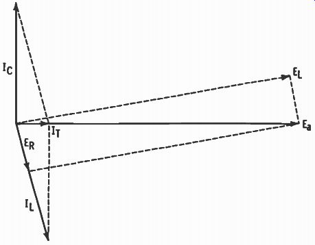
Fig. 6-4. Vector representation of a practical parallel LC circuit.
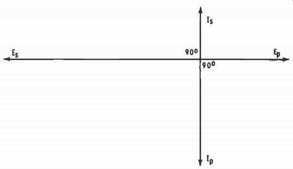
Fig. 6-5. Current-voltage relationships in transformers.
TRANSFORMERS
Vectors (phasors) can be used to show the current-voltage relationships in power or signal transformers, as in Fig. 6-5.
Primary voltage (Ep) is used as the reference because it is the voltage that is applied and thus initiates circuit activity. current through the primary winding lags the primary voltage by 90°, assuming pure inductance in the primary winding. however, inductive reactance is usually considerably larger than resistance so the phase angle approaches 90°. Voltage is induced into the secondary winding because the changes of current in the primary set up magnetic lines of force that cross the secondary. This induced voltage is maximum when the rate of change of primary current is maximum.
This occurs whenever the primary current cycle passes through zero in either direction. As a result of this inductive action the voltage induced into the secondary lags the primary current by 90°, as shown in Fig. 6-5. It could also be said that the secondary voltage has the same phase as the counter emf induced into the primary winding. The secondary winding is also inductive so that the secondary current lags the voltage by 90°, as shown, indicating that primary and secondary currents are 180° out of phase with each other.
As shown in Fig. 6-5, the transformer is connected step-up so that secondary voltage is greater than primary voltage.
Secondary current then is smaller than primary current be cause, neglecting losses, the product of primary voltage and current should equal the product of secondary voltage and current. However, the vectors shown do not apply in all cases, especially if the primary or secondary, or both, are tuned or if the transformer is loaded to any degree.
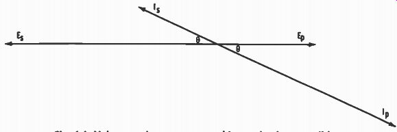
Fig. 6-6. Voltage and current approaching an in-phase condition.
As to loading, it is assumed with the vectors in Fig. 6-5 that only a very small current flows through the secondary winding, a condition of very light loading. If the load resistance across the secondary is decreased, the secondary current is increased, causing the secondary to appear more resistive. One condition of this is illustrated in Fig. 6-6. Voltage and current in the secondary approach an in-phase condition, assuming a parallel circuit analogy of source and load. Because of reflected impedance, the effective reactance of the primary is decreased, causing that circuit to also appear more resistive. This is true be cause Xi , and R act as a series RL circuit. As secondary loading (current) is increased, angle θ in Fig. 6-6 becomes smaller, causing voltage and current to more closely approximate an in-phase condition. An ideal transformer would have voltage and current in phase in each winding. The source would then work into a perfect resistance with maximum transfer of energy.
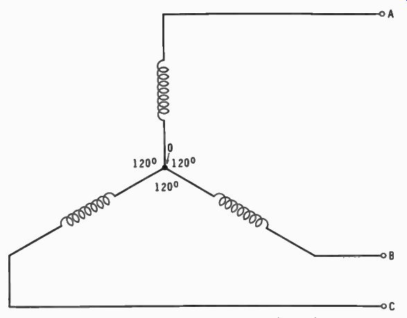
Fig. 6-7. One method of connecting three-phase coils.
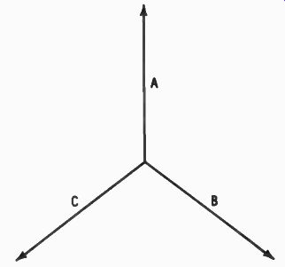
Fig. 6-8. Vectors representing Fig. 6-7.
THREE-PHASE POWER
Three-phase systems used primarily in power work include three separate voltages (or currents) , each separated from the other by 120 electrical degrees of phase difference. These voltages are produced from three separate coils (or windings) spaced 120° apart on the alternator. One method of connecting three-phase coils is shown in Fig. 6-7. This is a Y-connection (also called star) in which 0 is the common connection point, and one end of each of the coils is connected to this common point.
Vectors (phasors) representing these voltages are shown in Fig. 6-8. All the vectors are the same length, and they are spaced 120° from each other. The vector lengths are not drawn in a time relationship, because to do so, each voltage would have a different value, and each would be continuously changing with respect to the others. So these vectors can be assumed to represent some specific voltage, for example the rms value, of each of the separate phases. It could be added, however, that at any instant of time the sum of the three instantaneous values is zero, adding positive and negative values algebraically.
From the connection diagram (Fig. 6-7) it can be seen that the voltage between any two terminals is actually the voltage across two coils. Voltage AB, for example, is the voltage difference of coil-A and coil-B voltages. But these separate coil voltages are at 120° with respect to each other, and therefore cannot be added (or subtracted) directly. Vectors can be used to determine the multiplying factor for calculating terminal voltage. In Fig. 6-9 the voltage across coils A and B is solved by vectors. Other terminal voltages would be solved similarly with the same length of resultant.
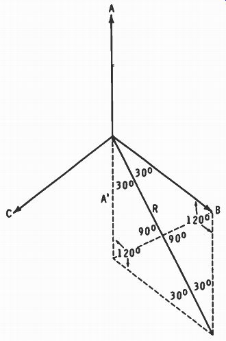
Fig. 6-9. Solving the voltage across coils A and 8 of Fig. 6-7.
A in the diagram has been reversed by 180° and is labeled -A'. The vector resultant is the diagonal (R) of the parallelogram formed from sides -A' and B. A was reversed because the terminal voltage is the difference (not the sum) of the separate coil voltages. Perhaps Fig. 6-10 may clarify this.
Two batteries are shown in Fig. 6-10A connected series-aiding.
With respect to 0 the upper terminal is -3 volts; and the lower terminal is +5 volts. With respect to the lower terminal the upper terminal is 8 volts (-3 -5) negative. But compare that to Fig. 6-10B. Here the upper terminal is -2 volts (3 - 5). In each case the voltages were added by changing the sign of one of them, which means that actually they were subtracted. The voltages could have been stated with respect to the upper terminal, but no matter which way they are stated the potential difference in Fig. 6-10A is 8 volts and that in B is 2 volts.
Referring back to Fig. 6-9 we see that a line has been drawn perpendicular to the resultant R. This line is the opposite diagonal of the same parallelogram, and with R it divides the parallelogram into four identical triangles. Vector B is the hypotenuse of one of them, and half of R is the side adjacent to the 30° angle. Cos 30° = .8660 so one-half of the length of R is .866 of the B voltage. So the entire length of R is 2 x .866, or 1.732 times, the length of vector B.
(A) Series-aiding (B) Series-opposing.
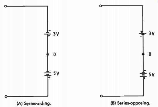
Fig. 6-10. Connection of batteries.
We can conclude from this that the rms voltage across terminals A and B is 1.73 times the rms voltage of either A or B. Resultant phase is a combination of the two separate phases, but it is not normally an important factor in power circuits.
It is the voltage that is of prime concern; however, in normal operation all three phases are used with the result that coil B is not only in the AB circuit, but it is in the BC circuit as well. And similarly, each coil is part of two different current paths.
TUNED-PLATE, TUNED- GRID OSCILLATOR
In the tuned-plate, tuned-grid (TPTG) oscillator feedback is accomplished through the plate-to-grid capacitance of the tube. And, as in any oscillator, the feedback must reinforce the oscillatory voltage and replace power losses in the tank circuit.
A typical TPTG circuit is that of Fig. 6-11 in which L1C1 is the grid tank and the oscillating section of the circuit. On the positive peaks of oscillation the tube is driven into conduction, and this, in turn, causes the L2C2 plate tank to also oscillate.
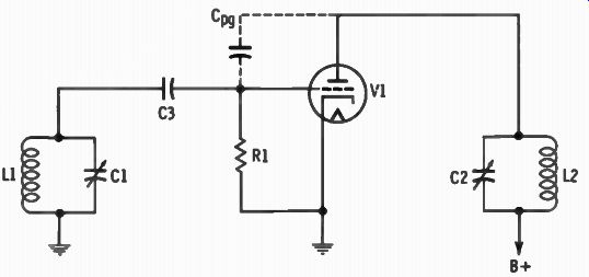
Fig. 6-11. A typical TPTG circuit.
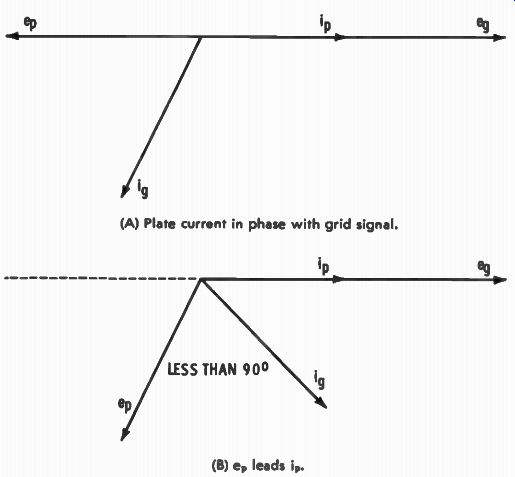
Fig. 6-12. Vectors of the circuit in Fig. 6-11. (A) Plate current in phase with
grid signal. (B) ep leads i_p.
To sustain oscillations, energy from the plate circuit is fed back to the grid in proper phase to replace the grid losses.
When the grid and plate tanks are both operated at the resonant frequency, they act resistively to the oscillation voltage on the grid. The plate current of the tube is therefore in phase with the grid signal, as indicated in Fig. 6-12A. Because of the normal phase inversion of the stage, plate signal (e ) and grid signal (e.) are 180° out of phase with respect to each other.
The plate signal also appears across the plate-to-grid capacitance and the grid tank as the feedback signal. But the reactance of the tube capacitance is much larger than the impedance of the grid tank (which is resistive) so the grid current (i g) leads e i , by nearly 90°. The voltage across the L1C1 tank circuit is in phase with i g, but the oscillations cease because the grid current is too far out of phase with respect to the grid signal.
When the plate tank is tuned to a higher frequency than the grid tank, the plate circuit acts inductively, so e i , leads i g as indicated in Fig. 6-12B. Plate voltage decreases when plate current increases so that the additional lead of e, places it be low the horizontal line as shown. The leading condition occurs because in the inductive plate circuit the voltage leads the current. The total lead is the normal 180° difference plus that caused by the inductive condition.
Again the reactance of the tube capacitance is much larger than the impedance of the grid tank, therefore grid current i_g leads plate voltage e_i , by nearly 90°. The voltage across L1C1 leads i g by nearly 90°, and the feedback voltage across the input is in phase with the original grid drive signal. In operation, the L1C1 tank operates as an inductive circuit because its Frequency is above that of the oscillation signal. The plate tank, however, is tuned to a higher frequency than the grid tank, hence it acts even more inductively. In this type of circuit the feedback need not be exactly in phase for oscillations to occur.
But the phase relationship must be close enough so that the grid losses are replaced, which allows oscillations to continue.
These latter statements can be shown to be true by the fact that there is a range of plate-tank settings, not just one particular setting, over which oscillations can occur.
PHASE MODULATION
A system of phase modulation, such as that of Fig. 6-13, can also be explained by use of vector relationships. In this circuit the RF and audio are applied across R1, R2, and R4 in series.
The RF input is labeled e g and appears across R1. C1 has low reactance to the radio frequencies, and the lower end of R1 is effectively at RF ground. The tube is cathode biased, but additional bias is provided by the audio voltage across R4. However, this audio signal is continually reversing polarity so that the R4 voltage alternately adds to and subtracts from the cathode bias. This means that total bias is changing with the audio signal, and the gain of the stage varies with the changes of bias.
The instantaneous plate load voltage is the resultant of two RF voltages. One of these is that coupled through the grid-to plate capacitance of the tube; this is labeled e l in the vector diagram (Fig. 6-14A). It is not in phase with e g, but it leads because the circuit is capacitive. The other plate signal is that supplied through normal amplifier action, and it is labeled e 2 in the diagram. It is 180° out of phase with e g, but the plate tank is at resonance and thus acts resistively. The resultant of these two voltages (e l and eo) is shown as e„ in Fig. 6-14A.
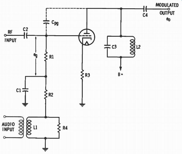
Fig. 6-13. A phase modulator circuit.
The amplitude of the amplified signal (eo) is relatively low because of the degenerative feedback that is produced as a result of not bypassing the cathode resistor.
When the audio swing is maximum, the gain of the stage is minimum, and e 2 has relatively small amplitude. Then e„ leads e a by phase angle θ. In the second vector diagram (Fig. 6-14B) the audio-signal swing has caused the bias to decrease and the gain of the stage to increase. The increased gain causes e 2 to increase in amplitude; it is labeled eo' in the second diagram.
This shifts the phase of the resultant e„ to that shown as e 0 ', changing θ to the value shown as 0'.
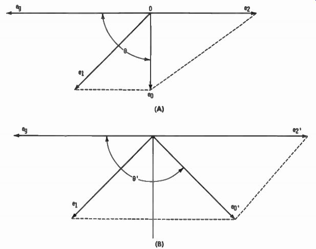
Fig. 6-14. Vectors of the circuit in Fig. 6-13.
In this way the audio signal causes the output to be phase shifted by an amount proportional to the audio amplitude. The greater the amplitude, the greater is the degree of phase shift that occurs. When phase-shifted, e 0 is applied to an oscillator tuned circuit, the time interval between signal peaks is shifted, thus phase modulating the carrier frequency. It is an indirect form of FM, achieving frequency modulation through altering the phase. Only one change is shown, but a continuous audio signal causes e„ to shift back and forth in step with the audio variations. The degree of shift is determined by the audio amplitude, and the rate of shift (number of changes per second) is determined by the frequency of the audio modulating signal.
DISCRIMINATOR
A discriminator can be used in an FM receiver to change a frequency-modulated signal input to audio voltage variations at the output. Fig. 6-15 shows an example circuit in which L1C1 is tuned to the intermediate frequency (IF) of the receiver. L1 is inductively coupled to L2L3, the center-tapped secondary, and L2L3C2 is also tuned to the intermediate Frequency. There is capacitive coupling from the transformer primary to the center tap of the secondary through Ce, the coupling capacitor. This voltage is developed across L4, with the center tap of the output circuit used as a reference point. Each of the diodes has two sources of voltage acting in series. For V1 the applied signals are those across L2 and L4; for V2 the applied signals are those across L3 and L4. Basic operation depends on the phase relations and the comparative conductions of the two diode circuits. By using vectors we can obtain a much clearer picture of the overall operation.
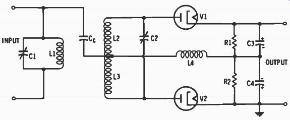
Fig. 6-15. A circuit in which 1.1C1 is tuned to the IF frequency.
ELI is the input signal voltage that has the same phase as EL. (Fig. 6-16A). The secondary voltage (E.) is 180° out of phase because of the 180° phase reversal of the transformer.
At the resonant frequency (IF) the secondary tank acts resistive so I. is in phase with E., the voltage causing it. The voltage across the secondary inductance leads the current through it by 90°, and with the center tap serving as a reference point, EL2 and E13 have opposite polarities, as shown. The reactance of L4 is high compared to that of coil L1 so that almost all the signal at the input appears across L4 in phase with ELi.
Fig. 6-16B shows the phase conditions existing when the resonant frequency (IF) is applied. EL, and EL4 are 90° out of phase with respect to each other; the voltage applied to the V1 circuit is the diagonal En . EL3 and EL. are 90° out of phase so that the voltage applied to the V2 circuit is the diagonal E2.
Equal magnitudes of voltage are thus applied across the diode circuits, the conductions are equal, and the voltage drops across R1 and R2 are also equal. But the currents through them are in opposite directions so the same potential exists at both output terminals. This means that when the unmodulated IF is applied the output voltage is zero.
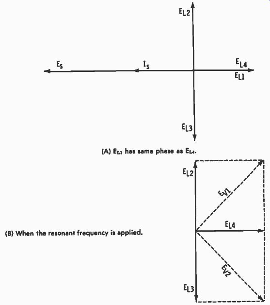
Fig. 6-16. Vectors of the circuit in Fig. 6-15. ( A) E LI has same phase as
E L. (B) When the resonant frequency is applied.
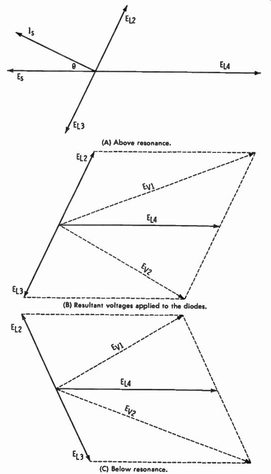
Fig. 6-17. Vector representation of Fig. 6-15 when the frequency is above
and below r . (A) Above resonance. (B) Resultant voltages applied to the diodes.
(C) Below resonance.
When the frequency of the input signal goes above resonance, - XL increases, X, decreases, and the L2L3C2 tuned circuit acts inductive. As shown in Fig. 6-17A, the secondary current (L) lags E„ by angle θ. The magnitude of θ is determined by how much above resonance the frequency changed. Secondary voltages across L2L3 are always 90° out of phase with respect to; therefore they shift as shown. E12 and E13, however, are still 180° out of phase with respect to each other. The EL4 reference remains constant and does not shift.
Fig. 6-17B shows the resultant voltages applied to the two diodes, and since En is greater than E.2, V1 conduction is greater than that of V2. This increases the voltage drop across R1 and decreases that across R2, resulting in an output that is positive with respect to ground. Below resonance the circuit acts capacitively so the shift is in the opposite direction, as shown in Fig. 6-17C. Then the voltage applied to V2 is greater than that applied to V1, and the voltage across R2 is greater than that across R 1. This results in an output that is negative with respect to ground. In every case the amplitude of the output signal is proportional to the change of frequency at the in put, effectively changing frequency variations into corresponding voltage variations.
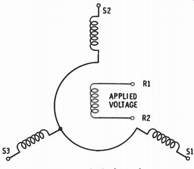
Fig. 6-18. Circuit of a synchro.
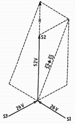
Fig. 6-19. Vectors representing the voltages in Fig. 6-18.
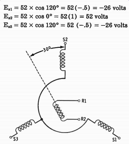
Fig. 6-20. Rotor has been rotated to 30°.
SYNCHROS
Synchros are motor-type devices, each having three stator coils and one rotor coil. The magnetic axis of each of these coils is separated from the other by 120°. They are Y-connected, but are not three-phase units. AC is applied to the rotor, as indicated in Fig. 6-18, and a voltage is induced into each of the stator coils. Magnitudes of these induced voltages are deter mined by the angular position of the rotor and the maximum voltage that can be induced. Stator voltages may be calculated by:
E„ = Ern x cos where, E„ is the stator voltage, En , is the maximum stator coil voltage, θ is the angle between R1 end of rotor and the stator coil.
Maximum voltage is induced when the rotor and a stator coil are in line with each other, for example, S2 in Fig. 6-18. At this rotor setting the synchro is assumed to be set at 0°. Minimum voltage is induced into a coil when the rotor is positioned at right angles to it. Assuming that the maximum stator coil voltage is 52, then:
E81 = 52 x cos 120° = 52 ( -.5) = -26 volts Ea -= 52 x cos 0° = 52 (1) = 52 volts Ea = 52 x cos 120° = 52 ( -.5) = -26 volts S2
Here the positive and negative signs do not indicate polarity; they indicate phase. If the voltage is positive, then it is in phase with the voltage at the R1 (reference) end of the rotor coil. If negative, they are 180° out of phase with respect to each other.
There are no in-between phases, they are either in phase or 180° out of phase.
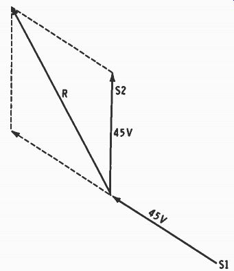
Fig. 6-21. Vector representation of Fig. 6-20.
The three stator voltages combine to produce a resultant magnetic flux in the direction the rotor is turned. Vectors rep resenting these voltages are in Fig. 6-19, each vector pointing in the direction of the positive end of the rotor coil. The resultant (R) is as shown, and it is in the same direction that the R1 end of the rotor is pointing. The length of the line is not important. It is the direction in which we are interested. However, at any angle the length of the resultant is always the same for a given synchro.
In Fig. 6-20 the rotor has been rotated to 30°. Remembering that for synchros, 0° is considered as being the direction of the S2 stator coil, the induced voltages are:
4,1 = 52 x cos 150° = 52 ( -.866) = -45 volts
E.2 = 52 x cos 30° -= 52 (.866) = 45 volts
Ea = 52 x cos 90° = 52(0) = 0 volts
Fig. 6-21 shows the vector representation with the resultant (R) at 30°, the same angle at which the rotor was set. This same process can be used for any angle, and in every case it gives the direction of the resultant magnetic field. When two synchros are connected together with corresponding terminals interconnected, any angular position set with one of the rotors is automatically followed by the rotor of the other unit.
There are many other circuits and systems which can be similarly analyzed by vectorial methods. Some of these are motors, generators, amplitude modulation, frequency modulation, phase-shift oscillators, coupled circuits, transmission lines, amplifier feedback, color-TV circuits, and multiplexing.