Article author Nigel Gardener is a consumer, automotive and packaging product marketing manager with National Semiconductor, Swindon. Prototype work by Mike Meakin.
-------
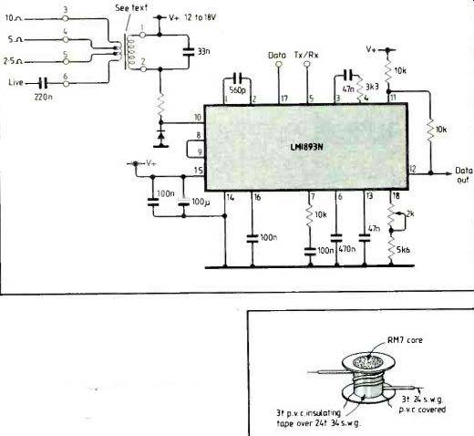
Fig. 1. Basic mains modem interface uses minimal components for complete
digital interface.
Fig. 2. Winding details for coupling transformer. Commercially available components are available.
-------------------
Frequency allocation proposed in draft British Standard
Band A 40 to 90kHz Reserved for electricity supply authorities
Band B 110 to 125kHz Continuously available channels for occasional transmission
Band C 125 to 140kHz Time-shared or burst mode, not continuous
Band D 140 to 150kHz Fire and security equipment
Power levels:116dB (µV) quasi-peak into 50 ohms, except band D which is 134dB(µV).
-------------
How to interface with the mains supply for data communication and expand into a cost-effective paging system
A number of articles have been published in the past showing `simple' methods of communication over the domestic mains. The general circuitry is simple enough for the data formatting prior to transmission, but the bugbear seems to be in the method of interfacing to the mains. One of the methods has been to inject the carrier signal between the neutral and earth. This suffers from one major drawback when the neutral and earth are bonded together at the electricity supply entry point.
The circuitry required for general interfacing tends to include a handful of transistors, regulators and passive components. Most of these components can be replaced by a single LM1893 circuit called a BilineTM carrier current transceiver. This circuit is a special type of f.s.k. modulator/ demodulator specifically designed for mains communications.
Circuit basics
With the impending release of a standard by BSI for communicating over the mains, there must be flexibility with the circuit design to enable the user to align the modem centre frequency within the allotted band. Table 1 shows the proposed frequency allocation. This may change when the specification is finally published, so any commercial user of this method of communication should check when the BS spec is published. The specification mentioned in the reference section was the only one available at the time of printing. However other countries will eventually produce their own specifications as this method of communication increases in popularity. Information about interference limits and test methods is contained in the Draft BS Spec listed at the end of this article. The LM1893 was designed to produce a sinusoidal output for minimum out of band harmonics.
The basic circuit for interfacing to the mains is shown in Fig.1. The transformer is either a Toko or Vacuumschelze type or a hand-wound design as shown in Fig.2. The Toko design can withstand about 2kV; the Vacuumschmelze and homebrew types should withstand about 4kV. An alternative method of isolation is shown in Fig.3.
This idea, originally published by Maplin in their Sept 1985 magazine, is a novel method of isolation. With slight modification to the mains transformer to include a dual secondary, a supply for the non-isolated circuit can be accommodated. Protection diode D5 is a transient absorber to prevent damage to the LM1893 by erroneous spikes on the mains and is an essential part of the protection circuitry for designs.
Simple control system
If a one-way control system is required, then Figs 4 and 5 could be a cost effective solution. The transmit circuit, Fig.4, is based around the 74C922 keyboard encoder, MM53200 garage door opener and the LM1893.
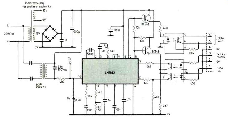
Fig.3. Novel method of isolation using opto-isolators.
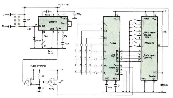
Fig.4. Basic mains control. Circuit diagram of keyboard encoder, parallel
to serial pulse width modulator LM1893 wired for transmit mode only.
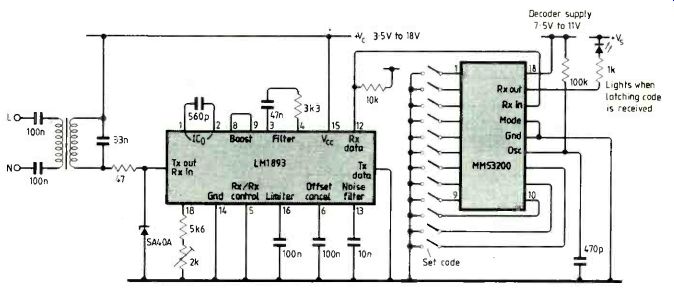
Fig. 5. Receiver for simple mains control. LM1893 wired for receive
mode only driving the MM53200 digital decoder.
Operation is straightforward enough. The user depresses a key which is then decoded by the 74C922. The four-bit output is presented to four of the 12 input data lines on the MM53200. The remaining eight bits of input data are used as a `house code' so that a number of controllers and slaves can work on the same system.
During a key depression, the data available pin (12) of the 74C922 goes high. As the output pattern from the MM53200 is of a continuous nature in this configuration, the LM1893 is used to gate the data stream onto the main by controlling its tx/rx pin. The drive for this pin is derived from a pulse stretcher made up from two gates of a CD4093 quad Schmitt circuit. The control input for this gating is obtained from the data available pin of the 74C922.
At the slave end, Fig.5, the LM1893 is used in the receive mode only. Again this can even further reduce the circuitry to around eight components. The data recovered from pin 12 of LM1893 is then passed directly to the MM53200 configured in the receive mode, i.e. pin 15 low. When four consecutive correct code sequences are received from the master, the output line is switched low.
This can be used to drive an led or with the addition of a transistor, any other load. The code for both master and slave must be the same, so the eight-bit ‘house code' needs to be the set with switches.
These two units form the basic circuitry for simple mains control. With some modification an answerback signal can be sent and received to indicate the required slave has switched successfully--see Fig.6.
When a key is depressed at the master end, the transmission sequence is sent via the LM1893; when released, the master reverts to the receive mode. At the slave end, data received and demodulated by the LM1893 is fed to the MM53200. When transmission from master to slave is finished, a valid output from the data output line triggers the monostable into echoing the selected slave address. At the end of the transmission, FF2 is clocked. This has two functions, one to switch the output load on and the other to toggle the DO address bit of the MM53200. This allows the n+1 number to turn off the slave by changing the least significant data bit. The FF2 circuitry can also be used on the simple set up of Fig.5.
When the slave address is echoed to the master, the transmitted and received patterns are compared and, if correct, the user receives an audible or visual signal confirming that the correct action has been taken by the slave.
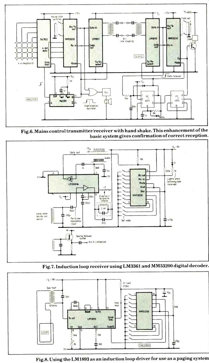
Fig. 6. Mains control transmitter/receiver with hand shake. This enhancement
of the basic system gives confirmation of correct reception.
Fig. 7. Induction loop receiver using LM3361 and MM53200 digital decoder.
Fig. 8. Using the LM 1893 as an induction loop driver for use as a paging system.
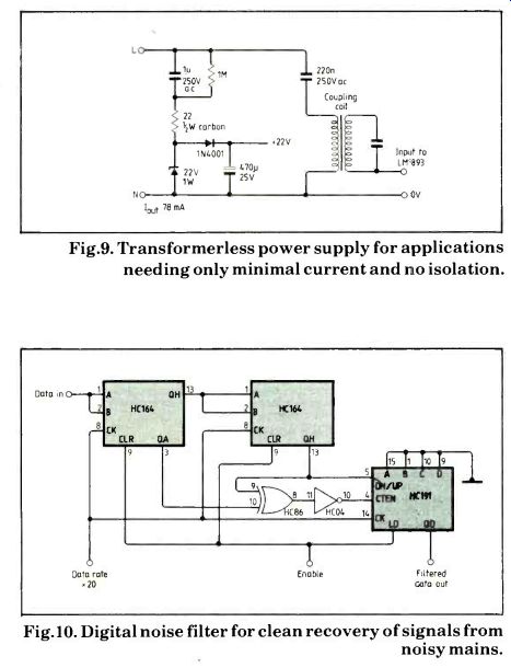
Fig. 9. Transformerless power supply for applications needing only minimal
current and no isolation.
Fig.10. Digital noise filter for clean recovery of signals from noisy mains.
And now for something completely different
Once the basic interface has been mastered, the expansion of the system is endless. On the master unit, for example, if mains connections from the Toko transformer are replaced with an inductive loop then the circuitry forms the basis for a very cost-effective paging system together with a suitable receiver, as shown in Fig.7 and 8. In this receiver, the signal is picked up by a ferrite rod aerial and fed to an LM3361 narrow band f.m. circuit. This device works to a low voltage with low power consumption. The output tuning is at the carrier frequency of 125kHz, achieved by padding out a 455kHz i.f. coil with a 2200pF capacitor. Recovered data is fed through the internal Schmitt of the LM3361 to provide clean data to the MM53200. An alternative power supply and interface is shown in Fig.9.
This transformerless circuit is intended for applications that do not have any connections exposed to the outside world.
Care in the choice of components is essential to ensure a margin of safety.
The LM1893 as it stands will work to 4800 baud, but if error checking is introduced the effective rate is reduced accordingly. For data transmission in areas where the background noise on the power lines could effect overall performance a digital filter, like that shown in Fig.10, could be employed.
This circuitry is currently being used on a commercial energy management system and has enabled the system to run at 2300 baud, with 144 bit data strings and a retransmission error rate of 0.01% over 1 million transmissions per day.
And finally…
These circuits for connection to the mains are intended to remove some of the pain associated with the transmission of data and control signals. The solutions given here are intended to give the interested engineer some ideas as to methods of interface. The medium for transmission is shown to be the domestic mains but the circuits will work just as well on a pair of wires dedicated as a networking bus. There will be less erroneous noise on a separate pair of wires and a reduction in transmission errors.
Further applications based on the simple interface with intelligence are intended, one being transmission of RS232 data from computers to one of a number of printers, another for interfacing a computer RS232 port to master control, which in turn controls up to 256 slaves. This is finished and will be published in the near future.
Each slave has four input, output and i/o lines for general interfacing to the outside world and forms the heart of an industrial or domestic control systems.
Watch this space for further details...
--------------
Further reading
Biline Carrier Current Networking Systems, National Semiconductor publication number 570075.
Carrier current protocol using an active repeater for consumer and industrial applications, Rob Lytle and Steve Strom.
National Semiconductor.
Mains tx/rx module, Electronics (Maplin Magazine) September 1985.
Draft standard for communication and interference limits and measurements for mains signaling equipment, British Standards Institute Draft Spec. No. 85/28596.
LM 1893 data sheet-linear supplement 1984, National Semiconductor.
Survey of mains signaling systems in the UK, ERA Technology, Leatherhead.
---------
Suitable transformers are type ZKB490/228-80-W insulated to 4kV made by Vacuumschmelze of Hanau D-6450, Germany and imported by Rolfe Industries (see advertisement), and Toko's 707VX-A0242YUK, insulated to 2kV and available from Cirkit Distribution.
----------------------
Also see:
Microcontroller chip integrates peripherals
Developments in packaging (Dec. 1986)
==========
(adapted from: Wireless World , Dec. 1986)