More features of a specially-programmed controller for evaluation and education.
By Mike Catherwood. Mike Catherwood is microprocessor applications section manager at Motorola's semiconductor products division, East Kilbride.
Peripheral functions and memory within the S2 single-chip microcomputer allow the device to be programmed to perform many tasks with very few components.
Last month's article described internal working of the chip and introduced a mask-programmed multi-function version made available only to readers of this journal. This S2 chip includes a monitor which can be driven by a terminal through a serial link, and routines for using the device as a pulse-burst generator, frequency meter and audio communication link using very little extra hardware.
Further routines are included for evaluating the data converter and watchdog time. This article describes using these and the speech-quality communication link.
Audio communication link
The internal eight-bit a-to-d converter and serial interface are used to digitize an audio signal and transfer the data between two S2 processors through a full-duplex serial link. Audio quality is surprisingly good, considering the limitations. Although this demonstration is of limited practical use because the serial interface is intended for local communications only, it forms a useful tool for illustrating some of the theoretical relationships commonly encountered in data communications.
For example the Nyquist criteria may be investigated by varying the low-pass filter cutoff points, or the effect on the signal-to-quantization-noise ratio may be observed by reducing converter accuracy through lowering the reference voltage. Relationships such as the Hartley- Shannon theory, which equates channel capacity to bandwidth and s-to-n ratio, may also be confirmed.
Software samples the a-to-d converter at 7.7kHz and the serial-interface clock is set to operate at 100Kbit/s (for a 4MHz m.c.u. clock). Information is therefore passed at a rate equal to eight times the a-to-d converter sampling rate which is 6Kbit/s. This is lower than the channel capacity of the serial interface and consequently the converter sampling rate is the communications-bandwidth limiting factor.
Two S2 demonstration devices are required for this application, one configured as a master (serial interface clock generator) and the other as a slave, Fig. 1. The serial interface is configured for three-wire (receiver, transmit and clock) full duplex operation.
One byte of data is exchanged between the devices every 131 machine cycles; received data is placed on port A which then drives a low-cost MC 1408L8 d-to-a converter Both input and output filters should have a cut-off frequency of less than half that of the a-to-d converter sampling rate, i.e. 3.8kHz for a 4MHz c.p.u. clock.
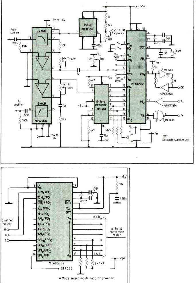
Fig. 1. One side of the S2 audio communication link. Lines C0,1 select
the converter channel as in Table 2. Line B5 reads low internally. 7
ne d.c. 'Set' potentiometer is set to provide an average converter input
d.c. signal level of about half way between VRL and VRH. For maximum
converter accuracy, VRH is tied to V and VRL to ground. Adding an expander
and compressor would improve s-to-n ratio.
Fig. 2. Analogue-to-digital converter evaluation. Three-bit digital code selects one of four channels or internal calibration voltages. For port B1 connections, see text.
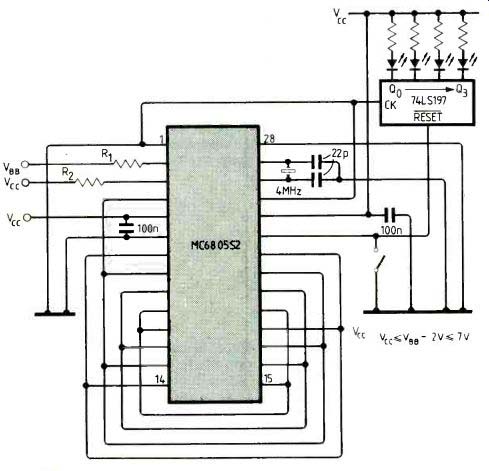
Fig. 3. Using the auxiliary counter as a watchdog allows the processor
to regain control after noise has caused erroneous operation.
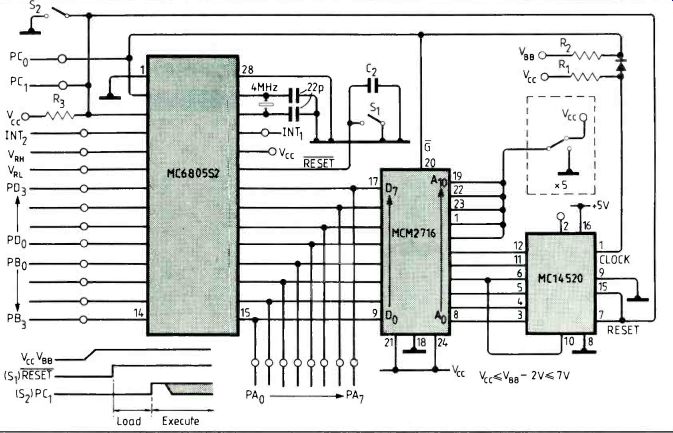
Fig. 4. Results of the S2 self-check routine are shown on four leds
(see Table 2). When the leds blink, the device has passed the test. To
run the self-check routine, port lines C0,1 are held high during reset.
Resistors R1,2 are 4.7k-ohm.
Table 1. Control codes for analogue channel selection.
Internal levels for calibration.
Table 2. S2 self-test indications
Switched-capacitor filters are easy to use and form effective low-pass filters. The c-mos MC145414 shown uses switched capacitors to form a dual fifth-order elliptic filter for low-pass operation. Two uncommitted op-amps are also included in the device.
Band limiting frequency of each filter is directly proportional to the input clock.
For example, an input clock of 128kHz provides a band-limiting frequency of 3.6kHz; halving the clock rate halves the band-limiting frequency.
Each filter is functionally identical except that one provides 18dB of gain within the passband and the other provides unity gain. In Fig. 1, an MC1455P1 timer is used in astable mode to generate a clock signal that can be varied between 70 and 180kHz.
Hardware for the audio communication demonstration was developed by Olivier Pilloud at Motorola's Geneva design centre.
A-to-d converter evaluation
This program allows you directly exercise the analogue-to-digital converter in the MC6805S2 and to accurately evaluate its performance in the intended environment.
Figure 2 shows how a typical test board could be configured. The analogue channel is selected by setting inputs, port lines C0,1 and Bo to states corresponding to a-to-d converter control register bits 0 to 2, as defined in Table 1.
After initialization, conversion of the selected analogue input is continuous. The channel selected may, however, be changed without resetting the processor since the program reads the channel code inputs before each conversion. The conversion result placed on port A bits 0 to 7 may either be the value after each conversion (port B1=0) or a value averaged over four conversions (port B1=1).
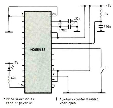
Fig. 3. Using the auxiliary counter as a watchdog allows the processor
to regain control after noise has caused erroneous operation.
Fig. 4. Results of the S2 self-check routine are shown on four leds
(see Table 2). When the leds blink, the device has passed the test. To
run the self-check routine, port lines C0,1 are held high during reset.
Resistors R1, 2 are 4.7k-ohm.
A data-valid strobe is also generated on port B to indicate when another conversion result has been output. It will rise and remain high during the period that the value on port A is stable.
Auxiliary counter demonstration
The auxiliary or watchdog counter is a ten-bit fixed-modulus counter which may be used in conjunction with some simple software to help ensure reliable processor operation in environments which would otherwise encourage erratic behavior. For example, should high-energy spikes appear on the power supply the m.c.u. may loose control and start to execute data patterns, causing a catastrophic system runaway.
A program using the auxiliary counter to avoid this regularly presets the auxiliary counter to its maximum value by inverting miscellaneous register bit 5. Provided that this is done more frequently than the auxiliary counter time-out period, then a forced reset will not occur.
So if a program runaway does occur it is probable that the auxiliary counter will not be regularly preset, resulting in the m.c.u. being reset at counter overflow and the user program being restarted.
In this demonstration the program simply increments port B. A hard-wired option enables or disables the watchdog option by manipulating the auxiliary counter reset-mask bit.
Therefore by operating two identical demonstration boards in the same adverse environment but with the watchdog enabled in only one, a direct evaluation of watchdog effectiveness can be made.
Wiring is shown in Fig. 3.
The auxiliary counter may alternatively be used as fixed-interval polled timer, provided that the auxiliary counter reset-mask bit is set. Even though the instantaneous counter value cannot be read by the processor, this feature may still be very useful in applications requiring long time-outs.
Self-test and bootstrap loader
Applying a voltage slightly in excess of V+2V to port line Co during reset causes the device o select an alternative of vecor on reset release, Fig.5.
The new reset vector points to the self-test program area.
Within this space, a bootstrap loader program also exists which allows you to copy small amounts of test code from an external eprom into S2 ram and then execute it. The level of port line C1 immediately after reset is released determines whether the self-test routine or bootstrap loader is executed.
Self-test involves execution of a sequence of subroutines for testing rom, ram, timers, i/o, a-to-d converter and interrupts on a cyclic basis. Many of the routines may be called by the user. Leds display the result of he test, Table 2.
The bootstrap loader program continuously copies data from an external eprom at address zero onwards into S2 ram at address 40 to 7F until port line C1 is pulled high. It hen executes a JSR 40 instruction and runs the loaded program. The most significant eprom address lines may then be incremented and the pro cess repeated with another user test routine.
Test results may be displayed on any of the spare ports.
This test procedure is obviously more flexible, but requires more hardware. Input/ output related tests are also difficult to realize properly.
Useful monitor subroutines
Figure 6 of last month's article shows hardware required for communicating with the S2's internal monitor through a serial link at either 300 or 1200 baud. Note that the 300/ 1200 baud switch is only sensed at reset.
Being in standard 6805 code, sub routines within the monitor and many of those used for the special functions will be useful to software writers. A full assembly-language listing is available.* Routines include low-level functions, such as writing/ reading a character to/from the terminal, and higher-level routines for reading and writing hexadecimal numbers for example.
Error conditions are usually indicated by the C bit being set on return from the subroutine.
Table 3 is a list of the more useful subroutines and a short description of what they do.
Any questions about how a particular subroutine works can probably best be answered by inspecting the source code.
In general, the subroutines shown in Table 3 try to preserve the registers that they do not use. Note that most of the routines expect to be able to use locations 5616 to 5B16 in ram. As the interrupt vector jump table resides 50 and 55, ram locations 50 to 5B should not be used.
Locations 40 to 4F are standby ram and are accessible if the ram is powered through port line D6.
In Fig. 8 of the September article, pins 17 and 18 should have been shown wired to OV; the V supply connects to pin 16 and pin 7.
Table 3. Useful subroutines within the S2 monitor.
Fig. 5. Small user programs in eprom can be loaded into he S2 using
this configuration. At reset, port line Co is held high and directly
after reset line C1 must be low. User code is executed when line C1 goes
high. Resistors R1,2,3 are 4.7k12.
*Assembly-language listings cost $4.00 from the editorial office. Please mark your A4 envelope ‘S2'.
----------------------
Also see:
Integrated pressure sensors in acoustics
Link | --Mains communication without tears
==========
(adapted from: Wireless World , Dec. 1986)