AMAZON multi-meters discounts AMAZON oscilloscope discounts
The field-effect transistor requires as much new thinking when comparing it to a bipolar transistor as is required when the bipolar is compared to the vacuum tube. The FET combines the advantages of the bipolar transistor and the vacuum tube. The FET has no heaters and thus requires no warmup time. The FET is tiny in size and consumes little power. Yet it is a voltage-operated device like a vacuum: tube , rather than a current device like the bipolar transistor. It has a high input impedance like a tube, not low like the bipolar. Therefore, an FET must be tested like a vacuum tube. While the bipolar transistor is tested in terms of beta , which is current, the FET is measured in terms of Gm or micromhos.
There is no emitter, base or collector in an FET. The emitter is the source, the base the gate and the collector a drain. The source, gate and drain compare more closely to the cathode, control and plate of a tube than the emitter, base and collector. There are NPN and PNP types , but they are called different names. The PNP is called an N-channel (Fig. 63) , taking its name from the center piece of semiconductor material. The NPN is called P-channel (Fig. 64) , taking its name also from the center piece of material.
The FET is built slightly different than the bipolar transistor. For instance, in an N-channel FET, there is a substrate of P material. The substrate takes the shape of a deep dish. In the deep dish is another dish of N material. Then in the recess of the N material is a plug of P material. The N material forms a channel between the substrate and plug of P material.
A lead is attached to one side of the N material. It is called the source. A second is attached to the other side of the N material. It is called the drain. If you apply a positive voltage to the drain and ground the source, current will flow from source to drain just like current can flow from a cathode to plate. A third lead is attached to the plug of P material. It is called the gate and more specifically is called the top gate. A fourth lead is attached to substrate. As expected, it is called the bottom gate.

Fig. 63. In an N-channel F ET, electron flow is from source (5) to drain (D)
and is affected by the gate (G) .
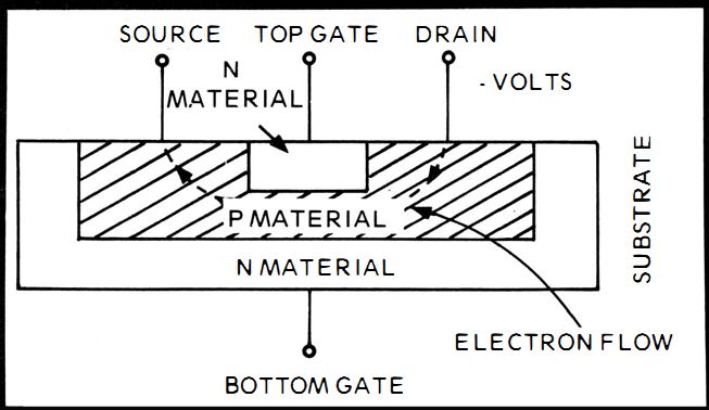
Fig. 64. In a P-channel F ET, the electron flow is from drain to source. The
gate serves as a valve.
While current is flowing from the source to the drain, if you apply a negative voltage to the top and bottom gate, you will narrow the channel and restrict the current flow. Should you vary the gate bias voltage with a signal, the channel will narrow and spread in accordance to the bias. In effect, you are modulating an electron stream in the channel just as a control grid modulates an electron stream in a cathode-to-plate flow in a vacuum tube. Amplification is the result. The small bias voltage causes a large drain current change. If the FET is a P-channel device, the source and drain polarities are reversed and the current flows the other way. However, the bias voltage is still negative and the gates narrow the channel to perform the amplification.
Schematic Representation
The FET just described is represented by a schematic symbol closely resembling a diode, except that there are three plate-type leads coming off. It is not at all like a diode so discard the similarity. The cathode-like part is the gate connection. The plate-like part is the channel. The top lead is the drain and the bottom lead is the source. The connections are appropriately lettered G, D and S. They should become as familiar as the bipolar E, B and C. If you remember that in a PNP the arrowhead is pointed at the base, designating the base material which is N, then when you see an arrowhead in an FET pointed at the channel, it too designates the channel material, in this case, N. In a P-channel FET the arrowhead points away from the channel, meaning P material, similar to an NPN bipolar that has a base of P material. The FET symbol just described has a solid channel line.
This shows that current is always flowing through the channel.
This always on channel is opposite to a normal off channel which is indicated by a broken channel line. This brings us to more terminology. Depletion and Enhancement Modes When the channel line is solid and thus always on, the FET is called a depletion type (Fig. 65 ). If the channel line is broken into three sections resembling three little plates, the channel is normally off and is called an enhancement type (Fig. 66). There are basically four types of ordinary FETs. The depletion N-channel , enhancement N-channel, depletion P-channel and enhancement P-channel.
Don't let the names throw you ; the names are more complicated than the function. To recap, there is a current flowing in the channel , one way for the N-channel and the other way for the P-channel. A negative bias tends to "deplete" the charge and by doing that retards the amount of current On the other hand, an enhancement type works something like a bipolar transistor. There is no current flowing in the channel. Current does not flow until a positive voltage is applied to the gate, which enhances the charge and the forward type bias, causing the current to flow in accordance to the level of the forward bias. A signal that is modulating the forward bias will modulate the current it causes to flow in the channel.
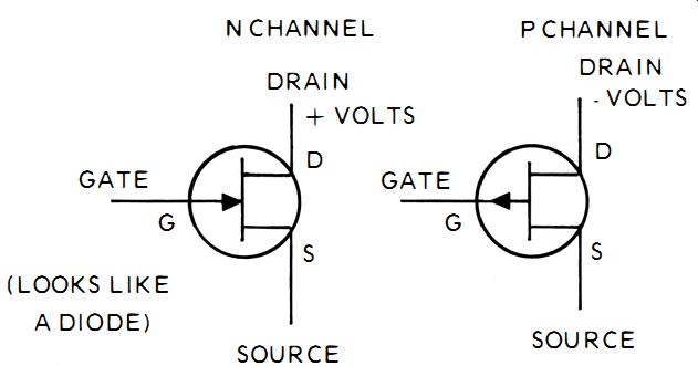
Fig. 65. Depletion-type FE T schematic representation.
The arrow points at N and away from P.

Fig. 66. An enhancement-type F ET has a broken channel line, but has the arrows
point like a depletion type.
There also is a depletion-enhancement type FET. In these types, a negative gate voltage will deplete the channel current or a positive voltage will enhance the channel current.
JFETs, IGFETs and MOSFETs
The JFET or junction FET is so named because the junctions between the N and P materials are the same as a junction bipolar transistor. They physically touch each other and form electrostatic barriers between the sections (Fig. 67). The barriers have a small amount of capacitance that varies with the voltage impressed as the barriers are slightly changed.

Fig. 67. A bipolar transistor has a depletion reg ion or barrier reg ion between
the material junctions.
The IGFET is so called because the gate is insulated from the rest of the device by a thin layer of dielectric material such as glass (silicon dioxide ). Therefore, this is not a PN junction between the gate and the FET, thus the name IGFET, insulated gate FET (Fig. 68 ). The MOSFET is just another name for an IGFET, but quite often it has more than one gate, typically dual gates (Figs. 69 and 70 ), The name comes from the dielectric material, metal oxide semiconductor. The gates are made of metal and are insulated from the FET by a silicon dioxide piece of insulation. They are all FETs , however. No. 72: TESTING FETs FOR Gm (HOOKUP) Whether the field-effect transistor is a JFET (junction FET) or an IGFET-MOSFET (insulated gate FET), the Gm can be easily tested with a transistor tester such as the Sencore TF151. The tests are made in or out of the circuit. If the FET has more than one gate, each gate is tested as if it were an individual transistor.
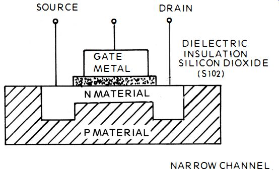
Fig. 68. An insulated gate FE T (IG-FET) has a narrow channel and the gate
is separated by a dielectric.

Fig. 69. A metal oxide semiconductor FET (MOS-FET) is so named because of
the oxide dielectric insulation.
Remembering that the names of the FET connections are the source, the gate and the drain (there is no E, B or C as in a bipolar transistor ), notice the connections. The black lead that went to the emitter now is attached to the source. The yellow lead that went to the base now goes to the gate. The red lead that went to the collector now goes to the drain. The analogy is borne out exactly by the tester itself.
No. 73 : IG-FET TESTING 2ND GATE FOR Gm (HOOKUP)
There is a separate lead for the second gate in an insulated gate on the Sencore TF151. It is blue and is attached to the second gate during the initial hookup. After the first gate is tested, the junction switch is then set on the second gate position. The same test is then repeated for the second gate.
No. 74 : JFET TESTING 2ND GATE FOR Gm (HOOKUP)
In a JFET, forget the second gate test. It is not applicable.
Simply short the two gates together and attach the yellow gate test lead to both the JFET leads. Test the JFET dual gate as if it were a single gate.
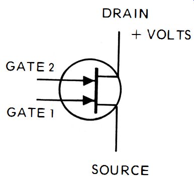
Fig. 70. The schematic diagram of a dual -gate MOS FET, N-channel type.
No. 75 : DEPLETION MODE BIAS TEST (HOOKUP)
The different types of FETs result in much confusion in determining appropriate test hookups. In a tube tester, there are so many different tubes that each is listed on a chart or in a guide and you simply turn switches according to numbers. In the transistor tester there are only a few tests, yet at the present time they are much more confusing than a tube tester. One of the confusions is based on whether the transistor is a depletion or enhancement type. Yes , the settings are listed in the reference book with the tester , but on many occasions the listing cannot be found easily. It's much better if you can determine the settings from the transistor and its schematic. On depletion type transistors , where a reverse bias is applied to the gate, the FET bias switch is placed on normal. This could also be construed as reverse , or negative.
No. 76 : ENHANCEMENT MODE BIAS TEST (HOOKUP)
In the enhancement type FET, the actual transistor must be (in most cases) an insulated gate type. Depletion types can be either JFETs or IGFETs. This is because depletion types , when they are JFETs, can use only a reverse bias, since a forward bias will cause ruining conduction between the gate and the channel, much like the vacuum tube control grid that draws too much current.
The enhancement type , since it is an IGFET, can have a forward bias. The bias cannot cause gate current to flow due to the layer of dielectric insulation between the gate and the channel. As a result, when you find an enhancement type FET, you can be sure it's an IGFET and you can apply a forward or positive bias. Set the FET bias switch to POS for positive .
No. 77 : FET TEST FOR Gm
Once you get the leads on the FET properly , set up the function switch and the correct bias polarity , you are ready for the actual Gm test. Set the Fm selector on Xl and the type switch on the N- or P-Channel type, whichever it is. The N-channel type arrowhead points to the N channel, while the P-channel type arrowhead points away from the P channel.
Press the gain button and read the Gm directly in micromhos. If the needle swings too far to the right, reset on X1O, reread and multiply the meter reading by 10.
No. 78 : SHORT TEST, SOURCE TO DRAIN
When a short develops from the source to the drain, since they are both simply connections on the opposite ends of a piece of semiconductor material, the material has broken down. It has changed its composition and become a conductor instead of a semiconductor. The tester needle will vibrate from the large amount of current being drawn through the meter from S to D. If the gain button is pressed, there is no gain registered. The FET keeps pulling the current .
No. 79 : SHORT TEST, GATE TO DRAIN
When a short develops between a gate and the drain, either the barrier in a JFET or the dielectric in an IGFET has shorted.
The unit is no longer a transistor but a resistor with three or four connections. The tester needle will vibrate from the current going to the wrong places between the channel and gate. No valid gain reading can be made.
No. 80 : SHORT TEST, GATE TO SOURCE
A short between the gate and source is quite similar to the short between the gate and drain. The channel is shorted to the gate , only at the other end. There will be less tester needle vibration since the drain voltage is not shorted to the gate. The source voltage is.
In some cases, according to the polarity of the channel, the source-gate and drain-gate shorts will appear the same. For instance, a short in a P-channel device between source and gate will appear the same as a short in an N-channel device between the drain and gate.
No. 81 : OPEN TEST, GATE DEPLETION TYPE
When the gate opens, it's as if a vacuum tube has an open control grid. The current through the channel will flow unimpeded by any gate bias voltage. The channel acts like a resistor with current flowing from source to drain. The meter shows erratic movement and cannot be zeroed since the bias. , from the tester has no effect on the FET.
No. 82 : OPEN TEST, GATE ENHANCEMENT TYPE
When the gate opens, no forward bias can be applied. No current flows through the channel without the forward bias.
Nothing happens with the meter. The needle just stays on zero, no matter what test is performed. The device remains completely passive and is cut off.
No. 83: OPEN TEST, SOURCE
When the source opens in either a depletion or enhancement type FET, the current is cut off and no Gm can be read. The meter needle simply stays on zero. The device is completely nonconductive. It's like an open cathode in a vacuum tube .
No. 84 : OPEN TEST, DRAIN
When the drain opens in either a depletion or enhancement type FET, the current is cut off and no Gm can be read. When the meter is zeroed, the needle does not move. The device is completely nonconductive. It's like an open plate in a vacuum tube. Incorrect Testing Quite often an attempt is made to test a transistor with the leads accidentally interchanged or a switch set on the wrong position. When that happens , false indications are given by the meter. Most technicians are familiar with what happens when a tube tester is accidentally set incorrectly. Following are the results of FET tests that are accidentally set up wrong.
No. 85 : .JFET BIAS POSITIVE INSTEAD OF NORM
When a depletion type JFET has a forward bias applied to its gate instead of a reverse bias , current can flow between the gate and the channel. If this happens, it's like a short between the source and the gate or· between the drain and the gate. Either no Gm reading will result or the needle will start vibrating and a very weak Gm reading will be indicated.
No. 86 : IGFET BIAS POSITIVE INSTEAD OF NORM
When a depletion type IGFET has a forward bias applied to the gate (POS setting ), nothing happens. The dielectric between the gate and the channel halts any DC current flow just as the dielectric in a blocking capacitor. The meter needle stays on zero and no Gm reading is recorded.
No. 87 : MOSFET BIAS NORM INSTEAD OF POSITIVE
If an enhancement type MOSFET has a reverse bias applied to its gate, instead of a positive bias, the FET does nothing.
No. 88 : SOURCE AND DRAIN LEADS SWITCHED
Should the source and drain leads become switched in either an N-channel, P-channel or the depletion or enhancement types, you'll never notice the difference during the test. All you are doing is reversing the direction of the current or hole movement. The channel is one piece of either N or P material and can conduct either way. You'll get a Gm reading and it will be accurate.
No. 89 : GATE AND DRAIN LEADS SWITCHED JFET N-CHANNEL
When the gate and drain leads are switched while testing a JFET N-channel type, you are placing a normal negative voltage from the gate on the drain and a positive drain voltage on the gate. The N-channel current is reversed and goes from drain to source instead of the other way. The positive gate voltage forward biases the drain-to-gate junction and the drain-to-source current flows into the gate. As a result the meter reads no Gm.
No. 90: GATE AND SOURCE LEADS SWITCHED, JFET N-CHANNEL
When the G and S leads are switched, the negative gate voltage is placed on the source and the source chassis ground is placed on the gate. This forward biases the source-to-gate junction. All of the source current flows into the gate instead of to the drain. The source and gate act like an ordinary forward biased solid-state diode. The meter will not read any Gm at all.
It's as if the source-to-gate junction were shorted. The meter zeros OK, but there is no needle movement.
No. 91 : GATE AND DRAIN LEADS SWITCHED, IGFET N-CHANNEL DEPLETION
TYPE When the G and D leads in this test are switched, the positive drain voltage is placed on the gate and the negative gate voltage on the drain. This causes channel current to flow from drain to source and the positive bias on the gate keeps the channel wide open. No current can flow from the channel to the gate in an insulated gate. As a result, the meter can be zeroed and it will read Gm accurately, but in a negative direction.
No. 92 : GATE AND SOURCE LEADS SWITCHED, IGFET N-CHANNEL DEPLETION TYPE
Should the G and S leads become switched in this type , the negative gate voltage is placed on- the source and the chassis ground source is placed on the gate. This places a forward bias on the source-to-gate, but no junction current can flow in an insulated gate. The current flows well from source to drain. The biases are the same as in an enhancement type FET. As a result, the channel current flows wide open and the Gm reading can be read, although it is not at all accurate. No. 93 : GATE LEAKAGE, JFET
Gate leakage to the channel is a very important FET parameter. Leakage in an FET is extremely low, normally.
Since a JFET is basically a 2-piece transistor (the gate and the channel) , a resistance reading from the gate to the source will provide a rough go-no go test.
The third part of the transistor is the substrate and is largely ignored during testing. A JFET has a resistance in the hundreds of megohms between the PN junction of gate and source. Any resistance reading at all on the ordinary shop VTVM is an indication of too much leakage. Compare any suspicious ohmmeter readings with the same reading on a "known good" JFET of the same type. Be sure to double check any resistance readings you get with the JFET in the circuit with one out of the circuit. A shunt resistance could be causing the suspicious resistance reading.
No. 94 : GATE LEAKAGE, IGFET
While a JFET has a multi-megohm reading across the PN junction , an IGFET has a resistance reading in the millions of megohms. The resistance test is identical to a capacitor go-no go resistance test. Any resistance at all on the ordinary shop VTVM means a defective piece of dielectric between the gate and the channel.
No. 95 : GATE LEAKAGE (IGSS)
The actual amount of IGSS is very important. It is quite similar to the amount of control grid leakage in a vacuum tube. Too much leakage can badly upset the function of a circuit. It lowers gain considerably and can introduce unwanted biases. Too much IGSS lowers the input impedance of the FET. IGSS should be tested in all new JFETs , IGFETs and dual-gate FETs before they are put in service. Some circuits can be very critical and, even though an exact replacement is being used, a slightly different amount of gate leakage will upset the circuit.
IGSS means the amount of current in microamps that manages to get from G to S. In a dual-gate FET, the number one gate leakage is designated IGISS and the leakage of the second gate is called IG2SS. Leakage should be tested with the device out of the circuit, because any amount of shunt resistance , no matter how tiny , can upset an IGSS reading.
The S, G and D are hooked up like a Gm test. The function switch is set at leakage and the type, either N or P channel, is selected. The leakage is read directly in microamps from the scale on the meter face. In most cases , any leakage at all means a bad FET.
No. 96 : GATE LEAKAGE (lG2SS)
If the FET is a dual-gate type, the function switch is reset to leakage IG2SS after IGISS has been tested. Even if the number one gate has no leakage, if the second gate shows some leakage, the FET is defective. Even the slightest movement of the meter needle usually means a defective FET, just as the slightest movement of the ohmmeter needle during a capacitor test means a leaking dielectric in a capacitor.
No. 97 : TESTING DUAL FETs
There are many dual type FETs ; that is, two separate FETs in one package. That means two source leads, two gate leads and two drain leads. The duals are tested in the same way as a single, only one at a time. If one section is defective, the entire unit should be discarded, unless you can mark, or cut off the leads of the defective unit and use the good one as a single FET.
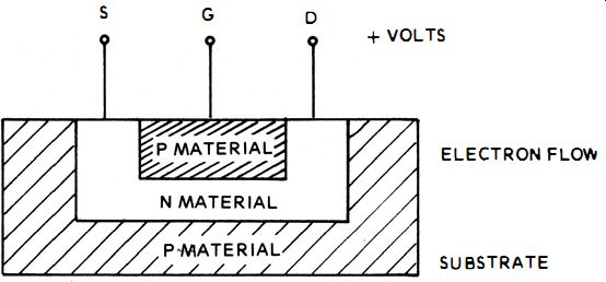
Fig. 71. The electron flow with the gate at zero bias is an important parameter,
IDSS.
No. 98 : MATCHING TEST FOR BIPOLARS
When matching regular or ordinary bipolar transistors to operate as a matched pair, certain parameters have to be tested. The transistors, of course, have to be the same type, NPN or PNP, and have similar or the same working voltages.
The critical parameters to check are the beta and ICBO (leakage between collector and base). The closer you can get these two parameters, the better the circuit, such as a push-pull audio output stage, will be balanced and thus deliver maximum, reliable amounts of power.
No. 99 : MATCHING TEST FOR FETs
When matching FETs to operate as a pair, in addition to the devices being the same type, N-channel or P-channel and the same build, JFETs, IGFETs, etc., the important match is IDSS, the "zero bias drain current. " (See next few tests.) When the IDSS is found nearly identical, check the Gm and be sure it is approximately close, too. The Gm, however, is not as critical as the IDSS.
No. 100: IDSS DEPLETION FET TEST
IDSS, called zero bias drain current, is the most critical FET parameter. During FET manufacture, many different IDSS ratings can occur in the same batch of transistors. The finished products are tested for IDSS and color coded like resistors or capacitors. When ordering replacement FETs, the color code must be specified. The color code also takes into consideration the Gm, but the IDSS is more important .
The test itself is like an ordinary FET test, except when you press the IDSS button you remove the negative bias from the gate and install a zero bias (Fig. 71 ). That makes the source to drain current flow at maximum intensity. The channel current is not depleted at all. The actual amount of current is read directly in milliamps from the IDSS meter scale. Typical values are 5 ma , 10 ma or 15 ma.
No. 10 1: IDSS ENHANCEMENT FET TEST
If you try the same test with an enhancement type FET, the test is not accurate. Enhancement type FETs do not attain maximum channel current until a high forward bias is applied to the gate. A special test setup is needed to apply a forward bias. However, such a setup is not a zero bias test.
You can get some use from a zero bias test, though. Some channel current will flow at zero bias. While it is not anywhere near a maximum current flow, the amount of flow will approximate the same number of milliamps in similar FETs. You can match similar FETs on an approximate basis in this way.
No. 102 : FET DISSIPATION TEST
Unfortunately, you cannot just solder an FET into a circuit as a replacement. You must calculate the amount of power dissipated across the FET, or else you can exceed the rating of the FET and blow it out in short order. The FET is rated to be able to carry a certain number of milliwatts ; for instance 50, 100, or 150. You can calculate the amount of power the FET must handle in the following way :
1. Measure the IDSS in milliamps .
2. Multiply that current by the resistance of the drain load resistor. You will get the amount of voltage dropped across the load resistor.
3. Subtract the load voltage from the source voltage, which gives you the amount of voltage dropped across the FET .
4. Lastly, multiply the FET voltage drop times the IDSS. That gives you the power dissipated.
If the power dissipated is close to or more than the FET rating, better get a stronger FET, lest it break down shortly in service.

Fig. 72. FET power dissipation is obtained by multiplying IDSS times the
FET load.
As an example of the above procedure, consider an FET rated at 75 milliwatts (Fig. 72 ). The IDSS is 10 ma. The voltage drop across the drain load resistor is 10v. The source voltage is 20v, which means the FET must drop 10v: 10v x 10 ma equals 100 milliwatts , which is too much for the 75 milliwatt rated FET. Better get a different one.
No. 103 : HUMAN BODY GROUNDING
The IGFET and MOSFET are quite sensitive out of the circuit to such an extent that ordinary handling-even with care-can ruin the device. You must observe care when removing them from packages and attaching test leads. Once the test loads are attached, the sensitivity is decreased drastically. The big danger is from static charges, even tiny hard-to-measure amounts of static voltage. You must ground the static charge in your body before touching them. Attach a clip lead from a ring or metal watch band to a chassis ground point on the test equipment that will be used. Then you can remove the device from the package .
No. 104: MAINTAINING SHORTED LEADS
The IGFET and MOSFET are packaged and shipped with the leads purposely shorted together. This reduces static charge danger. When attaching these devices to the source, drain and gate connections, keep the shorted leads in contact, until you make all the connections. Failure to do this could introduce a static charge and ruin the device .
No. 105 : SOLDERING PRECAUTIONS
Do not use a solder gun. Use as 10w a wattage iron as possible, just enough heat to melt the solder. Heat sink protection for the body of the device is a must. Attach a ground lead from the barrel of your soldering iron to the piece of test equipment that is being used. Be sure the test equipment has a 3-prong plug and is plugged into a correct wall plug that provides a good ground. Never solder an FET while the circuit has any power supplied at all. On occasion, a battery-operated circuit might be accidentally in an on position. If it's at all possible, remove the battery during the soldering operation.
No. 106: FET OSCILLATION TEST
Most transistor testers do not usually provide a means of checking an FET's ability to oscillate. Test manufacturers will argue that if an FET shows good Gm and leakage tests, it will oscillate according to its de-sing capabilities. However, this is not good enough when you are building an oscillator and want to be sure.
If you build a little grounded gate Colpitts oscillator, you can check the oscillation by installing a diode and microammeter in the source leg. The oscillator could be designed to run a t around 100 MHz, assuming that if it does run at that frequency, it will run at lower frequencies. With the circuit shown in Fig. 73, if the FET starts oscillating, the source current will be rectified and move the ammeter needle.
Different frequencies can be tested with different size drain feedback coils. An ammeter reading means the oscillator is running. No reading means it's not.
No. 107 : FET OSCILLATION LIMIT TEST
You can find out just how high a frequency and FET will oscillate by changing the drain feedback coils for others with fewer and smaller and smaller fewer turns. According to the rating of the coil , the oscillator will tend to run higher and higher in frequency. When you attach a coil and the oscillator will not turn on, the limit of oscillation of that FET has just been reached. The limit is between the last coil that did work and the one that won't work .
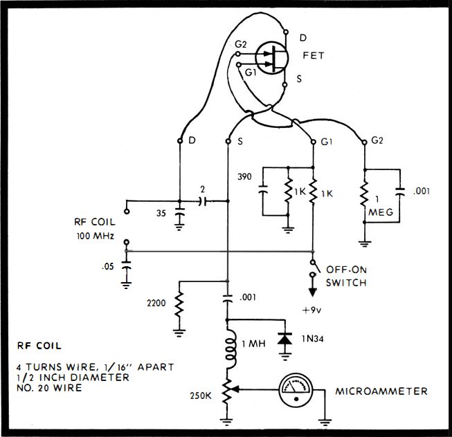
Fig. 73. You can tell whether or not an FET will oscillate by connecting
it to this circuit.
No. 108: TRANSISTOR-FET FREEZE TEST
When a transistor or FET is suspected of intermittent operation, the freeze test frequently will make the defect appear. Attach the transistor tester to the suspect while in the circuit. Keep the equipment turned off. Take a beta or Gm reading at this static condition. Note the reading.
Then spray freeze the transistor. Wait until the frost appears on it and press the gain button again. If the beta or Gm is just about the same, the transistor is testing OK. However, if the gain changes drastically or no reading at all is obtained under the freeze condition, the transistor is defective.
No. 109: TRANSISTOR POTENTIOMETER TEST
When testing a transistor in a circuit, if there is a potentiometer in the base circuit, such as a volume control , you can use it to verify a test.
When the pot is across the base without a blocking capacitor, it is a variable shunt resistor (Fig. 74). With the transistor tester attached in the circuit (with the equipment turned off ), take beta readings at different pot positions. At minimum, when the pot is shorting out the base, the transistor will act as if it is shorted. As you then vary the pot , different readings will show up on the meter. This is normal.
If the same readings keep showing, the transistor is defective. Also make sure that you do not inadvertently take what you consider is a valid reading while the pot is shorting out the base at its minimum setting.
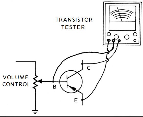
Fig. 74. Be careful when making a transistor test in circuit. Look out for
any low resistance or pots in the base.
No. 110: LO-POWER OHMS FUNCTION TEST
Every technician has had to go through the trouble of disconnecting components in a circuit in order to make a resistance test. Of course, it is much easier to make in-circuit tests. In tube-type circuits it's easy to make in-circuit tests by figuring what resistance is in a circuit that is being measured.
In transistor circuits this ability runs into a complication.
The normal 1.5-volt battery causes enough current to flow in the circuit to turn on the transistor (Fig. 75). As the transistor conducts , the ohmmeter needle arrives at incorrect posit ions. A 100K resistance can read anywhere from a few K to 100K, according to the point where the meter is connected. There is a way to avoid the problem and still be able to test in-circuit.
Germanium transistors turn on when a forward bias is applied with a voltage of about 0.2. Silicon transistors turn on with 0.6 volt. In order to be sure , the 1. 5-volt battery output must be reduced to under 0.1 volt. Lo-power ohmmeters are appearing on the market (the Sencore FEI60). They provide an ohmmeter voltage at the test probes of no more than 0.08 volts. This is low enough not to turn on any transistors. In circuit tests can be made without getting false readings.
The 1.5-volt output has to be available , too, since many of schematics show resistance and back-to-back measurements dependent on the 1.5-volt output. The Lo-power function though, can be used in many, if not most, applications.
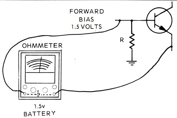
Fig. 75. Conventional ohmmeters with 1.5v batteries turn on a transistor during
a routine ohmmeter test and makes the test worthless.
No. 111: AN EVEN LOWER POWER OHMS TEST
Even though the general rule is that germanium transistors need 0.2 and silicon needs 0.6 volts of forward bias to conduct (Fig. 76 ), large, heavy current transistors made of germanium will turn on at the Lo-power 0.08 volts. There are always exceptions. How can these transistor circuits be tested? You can lower the battery output even more with a high value resistor. It has been computed that if you put a 100K resistor in series with the line, the voltage is reduced to 0.008 volts. An isolation probe such as this is usually available with a Lo-power ohmmeter.
No. 112: SMALL THERMISTOR TEST
Small thermistors, which are being used more and more in solid-state circuits , are difficult to test with a conventional ohmmeter. Thermistors are usually rated at their higher "cold" resistance. As they heat in use , thermistors drop in resistance. If you measure them hot the resistance reading will not be correct.
If you use a Lo-power ohmmeter, the low voltage output of 0.08 volts does not provide enough current to pass through the thermistor to heat it up and thus lower the resistance. It turns out the only way you can test the thermistor is by using the Lo power ohmmeter .
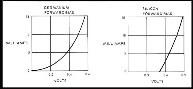
Fig. 76. Germanium transistors turn on as the forward bias approaches 0.2
volts. Silicon needs about 0.6 volts.
No. 113: FIGURING DIODE POLARITY
During servicing, diodes have to be replaced and it is rare that the available replacement is identical to the original. They come in all types , sizes and shapes. It is important that you replace a diode with the same polarity as the original. If you don't, the diode might not work and could even cause an electrical dead short.

Fig. 77. Diode polarities can be confusing since they are marked positive
on the cathode and negative on the anode.
Some confusion exists in the replacement situation.
Diodes are marked plus and minus. The plus is on the cathode and the minus is on the anode. This is opposite to the forward bias power supply voltage that is usually provided. The power supply provides a plus voltage for the anode of a tube or solid-state diode and a relative minus voltage to the cathode for forward biasing.
The plus on the diode cathode means there will be a lack of electrons there and an excess of electrons on the anode (Fig. 77). The electron flow will be from the area of insufficient electrons on the plus cathode to the area of excess electrons on the minus anode. That is forward bias.
When you see a diode symbol, it looks like an arrowhead against a bar. Forget the arrowhead idea. Think of the object as a triangle. The bar is the cathode and the triangle is the anode. Forward bias-on the diode is shown on the ohmmeter as a low resistance. Reverse bias on the diode is indicated a high resistance. Forward bias causes electron flow from plus to minus in the diode. Reverse bias prevents electron flow from minus to plus in the diode.
No. 114 : TESTING DIODE IN-CIRCUIT
Most transistor testers check diodes and power rectifiers right in a circuit, which is handy since it avoids some soldering.
With the equipment off, the emitter lead is attached to the cathode of the diode. The collector lead is attached to the anode (Fig. 78 ), The type switch is set on NPN. Some current will flow through the semiconductor material. Turn the calibration knob fully clockwise. If the meter will go upscale, the diode is working and is capable of diode action.
If it won 't move, it is either shorted or open. Then you can remove it from the circuit.
No. 115: TESTING DIODE OUT OF CIRCUIT
Once you get an indication that a diode is bad, or you want to test a new one before installing it, an out-of-circuit test will verify its quality in a definite manner.
The leakage test position of the transistor tester provides the accurate test. Attach the base and collector leads to the cathode and anode of the diode. Then switch the type selector from NPN to PNP and back (Fig. 79 ). A good diode will read on opposite ends of the scale for each setting of the type switch. It's an excellent go-no go test of forward and reverse current.
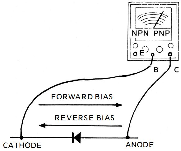
Fig. 78. Diode polarity ca n be determined with the B and C transistor tester
leads. Forward bias will deflect the needle.

Fig. 79. Diodes ca n be tested out of circuit by attaching to Band C tester
leads.
No. 116: GRADING THE DIODE
A good diode used in audio or a video detection type should have a forward-to-reverse micro-amp current ratio of at least ten to one. The preceding test , if read carefully, will tell you if the diode is satisfactory or not. A good germanium diode should not read any more than 40 or 50 micro-amp reverse current. The meter reads it directly. Forward current should be at least 500 microamps or bet ter. The heavier duty silicon rectifier should have an even higher ratio. A good one will show 4 or 5 thousand microamps in the forward position and absolutely no leakage on the ordinary transistor tester (it's too small to measure with that instrument) on the reverse bias setting.
No. 117: VARICAP DIODE TEST
One of the most important tests of a varicap diode is its reverse current leakage. This is easily accomplished on the transistor tester. Too much reverse leakage ruins the variable capacitance effect of the special diode. It's not enough to know that the diode is working ; it's how well it is working. It is used in frequency-sensitive locations and can kill sensitivity, output or correct frequencies. A varicap is like a silicon diode and should read practically none, or actually no reverse leakage on the ordinary transistor tester. Attach the diode to the base and collector leads (Fig. 80 ). Try both NPN and PNP positions. One will read forward and the other reverse leakage. A good one will read no reverse leakage. Even a little reading indicates the diode could be in poor condition for its job.
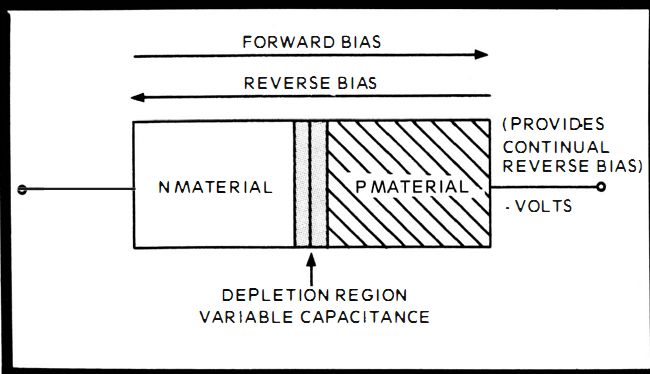
Fig. 80. A varicap diode is opera ted only with reverse bias. During forward
bias there is no variable capacitance.
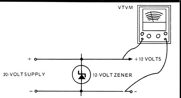
Fig. 81. A zener diode can be tested by installing it in a test circuit, with
cathode toward the positive voltage.
No. 118: ZENER DIODE KNEE VOLTAGE
During construction of electronic gear, or servicing , you might get a zener diode without markings. While it might be the unit you need, it's risky to install it in a critical circuit unless you know that it is operating properly.
Zener diodes are made of silicon with a very special characteristic. In fact, the applications for zener. diodes do not resemble ordinary diode applications at all. The ordinary diode has the job of changing AC to pulsating DC, or rectification as it's called. The zener diode is a voltage regulator.
It keeps a voltage at a specified reference level, no matter what amounts of current are passed, within the operating limits of itself.
Usual silicon zeners can control voltages from one on up to hundreds of volts. The power ratings can be as low as a fraction of a volt on up to a hundred or two volts. Zener diodes are like other silicon diodes except for one characteristic. At a particular voltage in the reverse bias condition, the zener suddenly stops being a high resistance to electron flow and becomes a tiny resistance. This causes a heavy current flow at this voltage and no matter how much more voltage is sent in, the heavy current flow continues and holds the voltage at that particular point. The voltage where the zener turns from a high resistance to a small resistance, where the sharp break causes the sudden heavy conductance, is called the zener "knee." The word is taken from the appearance of the graph curve of the characteristic. That knee voltage also designates the name of the zener. For instance , it could be called a 12-volt zener , or a 190-volt zener.
To test a zener, get a power supply, a radio , TV, or any kind of electric unit that provides a voltage that is somewhat higher than the voltage the zener rating (Fig. 81 ). Turn on the supply and take a voltage reading of the DC output across the load. For instance, suppose it's a 20-volt supply and you are going to test a 12-volt zener. You'll test first and make sure there is the correct 20 volts across the load.
Next, attach the zener cathode, which might be marked plus , to the 20-volt end of the power supply. Attach the zener anode, which might be marked, negative, to the ground or the supply chassis , whichever is B minus.
Then turn on the supply and take another voltage reading.
This time the power supply will come on, but measure only 12 volts. The voltage , since it exceeded the knee of the zener , simply pumps current through the zener as current was pumped the voltage dropped. At the 12-volt setting, the amount of current is stabilized. Only a certain amount of current flows because as the voltage goes below 12 volts, the zener shuts off conduction. As the current tends to stop, the voltage stops dropping. The zener has many uses and is becoming a common component.

Fig. 81 A. The zener knee represents the ma in characteristic of a zener diode.
Conventional diode activity is not used.

Fig. 82. By installing a known good resistor across another resistor, they
form a parallel circuit and subtract if the original resistor is OK.
No. 119: COMPONENT SUBSTITUTION TESTS
One of the surest ways to test a suspected component is to clip a known good component of similar value into its place. The various so called "decade boxes" are devices that offer many component values through clip leads. There are substitute resistors , capacitors, rectifiers and filters all built into a handy unit. When you suspect a component, all you do is disconnect one end of it and attach the clip leads in its place. If the electronic unit returns to normal operation, the test has proved the suspected disconnected component was defective. This test is so effective that many electronic units are repaired every day without use of any other test equipment or even knowledge of theory on the servicer's part. This "snip and clip" test also can be used with actual components, but a decade box is much handier and reliable.
Component In-Circuit Bridge Tests
There are many in-circuit tests that can be made using a component, either singly or from a decade box. These are bridge tests and no disconnection of parts is needed. These tests are limited in scope, due to the fact that the circuit is not opened. Fortunately , though, the tests are valuable since they find a large percentage of bad components.
No. 120: SUBTRACTING RESISTANCE TEST
One of the major resistor failures is an increase in value or an open which makes the resistance infinite. The resistor becomes suspect when a wrong voltage appears on a cathode , collector , etc. The voltage can be high or low, depending on the position of the resistance in the circuit.
If there is nothing in shunt with the resistance, it can be measured directly with the ohmmeter. However, more likely than not, there is usually something in shunt. A good test is to bridge the resistor with another of the same value (Fig. 82). According to basic mathematics , if the resistor is good, you'll be providing an additional path of the same value for the current and, therefore , cutting the resistance in half.
If the resistor has increased considerably in value , the substitute resistor will carry most of the current flow. In effect, you have subtracted resistance from the suspect. A recheck of the voltage on the test point is appropriate. If the voltage has become normal, the suspected resistor has definitely increased in value and is defective.
No. 121 : ADDING CAPACITANCE TEST
A capacitor can fail in one of four ways. It can short completely , develop a high-resistance short, open, or change in capacitance value. The addition of capacitance as a test indicates three out of the four types of failures, but it can't help a dead short.
You can add capacitance directly to an in-circuit capacitor by simply bridging another similar unit across it (Fig. 83 ). For instance, if you bridge a .05-mfd capacitor across a suspect, you add .05 to it. If the capacitor has a high-resistance short , it is no longer a capacitor but a resistor of that value. If the capacitor has opened, it's just an open connection. Should the capacitor have changed value, it always changes to a much lower value. Adding capacitance in any of these cases provides a positive indication of a defective capacitor .
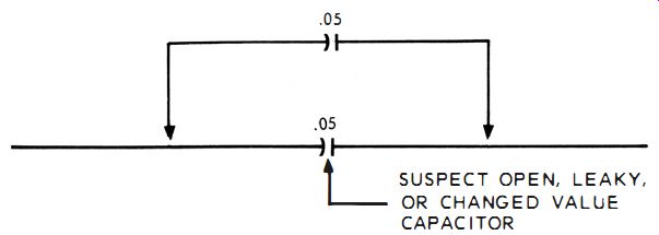
Fig. 83. By installing a known good capacitor across another capacitor values
add.
No. 122: ADDING RESISTANCE TEST
While resistance can be subtracted without unsoldering , adding resistance usually entails the use of a soldering iron , unless the test spot is some form of plug-in. It is necessary to add resistance to the circuit if a suspect resistor has decreased in value, or if you are building a kit and feel you need more resistance at a particular spot. Then you must unsolder one end of the existing resistor. If one end is on the chassis, that's the end to unsolder. Try not to unsolder any connections directly to a heat-sensitive device like a transistor. In tiny circuits, be sure to heat sink as you unsolder. Once an end is disconnected, you can add resistance by attaching the substitute between the loose end and the point where it was connected, or substitute another resistor or the entire disconnected resistor.
No. 123: SUBTRACTING CAPACITANCE TEST
An existing capacitor can be lowered in value by putting another capacitor in series with it. If they are both the same value , the capacitance will be halved. Once a capacitor end is disconnected, you can add another capacitor to it, and a certain amount of capacitance will be subtracted, depending on the value of the added capacitor.
No. 124 : IN-CIRCUIT TRANSISTOR AUDIO WAVEFORM TEST
Any transistor that has to pass an audio frequency can be tested in the circuit under dynamic conditions with a signal generator and an ordinary scope equipped with a high-impedance probe. By putting a sine wave in and viewing what the sine wave looks like when it comes out of the transistor, you'll get an idea of the transistor 's quality.
Attach the generator output, through a capacitor larger than the base input capacitor in the circuit, into the base of the transistor. Set the generator for an audio output around 1 kHz, turn on the generator and the amplifier. Attach the scope probe to the amplifier output and set the scope to display the 1 kHz generator signal. Observe the scope display. One of four things will happen. One, the sine wave will be excellent. Two, the positive peaks will be clipped. Three , the sine-wave negative peaks will be clipped. Four, both peaks will be clipped (Fig. 84). If it's one of the last three, the transistor is not working properly. Try a few different ones until you get a perfect sine-wave display on the scope.
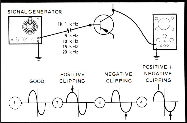
Fig. 84. The amplification and frequency response of an audio amplifier can
be checked with a signal genera tor and a scope.
No. 125: IN-CIRCUIT TRANSISTOR AUDIO FREQUENCY RESPONSE TEST
Using the same test setup mentioned in the previous test, once you have a good transistor passing a I-kHz sine wave, set the signal level at a normal listening level. Then start raising the frequency in steps up to the rated frequency response of the amplifier. For instance , if it's an FM receiver producing audio up to 20 kHz , raise the frequency in steps , like 5 kHz, 10 kHz, 15 kHz and then 20 kHz. Observe the sine wave. Some clipping will occur, but if the sine wave remains basically the same, all the way up the scale, the transistor is good. Should the sine wave start clipping at a lower frequency, it's not responding properly.
No. 126 : POWER TRANSFORMER OUTPUTS
Power transformers are found in a variety of electronic gear and serve many complex applications. Usually , it has a single primary and a step-up secondary for B+, step-down secondaries for various heater requirements and a center-tapped secondary for full-wave rectification. These voltages have to be tested.
The voltmeter is set for AC and the probes are attached to the various test points in the transformer. If the 117v AC is correct going in, then the secondaries should have appropriate voltages ; for instance, 250v AC across a step-up secondary and 6.3 volts or 5 volts across a step-down secondary.