by JAMES J. BARBARELLO
This mini analyzer is inexpensive, versatile, and easy to build.
AFTER YOU HAVE COMPLETED YOUR latest logic circuit design, you will probably want to build a prototype to test its operation. If the circuit is not complex, a common logic probe is all that's needed to troubleshoot it. however, if the circuit has multiple signals that must be checked for proper time phasing, or if it requires one or more complex driving signals to exercise its operation, then you need a more powerful testing tool.
Professionals use a logic analyzer and function generator to make these tests. Experimenters, hobbyists, and those on a tight budget will want to build the PC Mini Logic Analyzer. It costs only about $30 to build, but when it is linked to an IBM compatible computer, it is sufficiently capable for most hobby applications. The PC Mini Logic Analyzer provides up to eight driving signals (outputs) and eight inputs. Each output can be programmed with up to a 64-bit pattern. In addition to its logic analyzer function, the unit can serve double duty as a digital integrated circuit (IC) tester.
The analyzer consists of a hardware interface with applications software. The interface buffers the signals that are sent from the computer's parallel port to the circuit to be test ed. It also buffers signals that are returned fro the circuit to the computer, and shifts their voltage levels so that they are compatible with the PC's logic levels. The Interface obtains its power from the circuit under test, so it will always recognize the proper logic levels: TTL at 5 volts, or CMOS from 3 to 15 volts. The interface can be connected directly to any parallel port on your PC.
The software displays 64 bits of the eight outputs and eight inputs simultaneously. It allows full on-screen programming of the outputs. Scan time (the time to process the 64 bits) can be adjusted from a high of about 100 bits/second on an average PC to a low of one, bit every 10 seconds. The slower speeds al low you to single step through a circuit and observe how each output bit affects the prototype circuit's operation.
Best of all, the interface circuit is composed of common components, all available from most electronic component suppliers. Although a PC board layout is provided here, it is not essential for proper operation; the circuit can also be constructed on a solderless bread board.
The hardware interface will be described first, followed by the software. Then, an actual logic analyzer application will be described, followed by an example of how to use the analyzer as a digital IC tester.
Theory of operation two basic functional blocks; a transistor buffer/inverter section, and an analog switch section that feeds voltage comparators. The transistor buffer/ inverter section is shown in the schematic in Fig. 1.
Transistor Q1 in Fig. 1 is con figured as a standard inverting switch. A signal greater than about 0.7 volt from the parallel port (pin 2 for Q1) causes the transistor to conduct, raising the output (01 for Q1) to about 0.3 volt. When a signal less than 0.7 volt is applied, the transistor does not conduct, and current is provided to any load connected to the output through the collector resistor (R2 for Q1). This signal inversion is compensated by the soft ware. For example, when the user requests a high logic level to be output at 01, the software converts the request and outputs a low logic level at pin 2 of the parallel port. The transistor will invert that low logic level to a logic high, producing the output requested by the user.
The transistor inverter/buffer performs two necessary functions. First, it acts as a current amplifier, providing more current than the parallel port could provide directly. Second, since the transistor obtains its operating voltage through D1, the output levels will be consistent with the logic levels generated by the circuitry that is supplied by that voltage. (The output voltage level is not dependent on the input driving voltage, which will always be that provided by the parallel port).
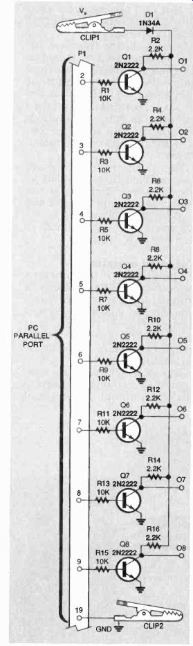
FIG. 1--THE ANALYZER incorporates two basic functional blocks. This is the
transistor buffer/inverter section.
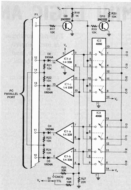
FIG. 2--THE ANALOG SWITCH SECTION feeds the voltage comparators. Two of the
analog switches in a CD4066B quad-analog switch IC (IC2-a and IC2-b) feed their
outputs to the non-inverting input of IC1-d, one of the four voltage comparators
in an LM339 quad comparator IC.
Diode D1 protects the inter face against reverse power sup ply voltage. The approximately 0.3 volt lost across the diode is insignificant in the operation of the interface. The transistor inverter/buffer is used eight times (Q1-Q8) to provide eight outputs.
The second functional block is shown in Fig. 2. livo of the analog switches in a CD4066B CMOS quad-analog switch IC (IC2-a and IC2-b) feed their outputs to the non-inverting input of IC1-d, one of the four voltage comparators in an LM339 quad comparator IC. When the control pin of an analog switch is pulled high, the switch will pass the input signal to its output, also putting from about 50 to 200 ohms in series in the pro cess. When the control pin is brought low, the path between input and output becomes a very high impedance, effectively disconnecting the input from the output.
The signal from pin 1 of the parallel port is inverted twice, once by transistor Q9 and a second time by Q10. Therefore, the control signal for analog switch IC2-b is 180° out of phase with the signal for IC2-a. With a high signal at pin 1 of P1, switch IC2-a will be on, and IC2-b will be off.
Conversely, with a low signal at pin 1 of P1, the switch IC2-a will be off, and IC2-b will be on. This allows the two switch outputs to be connected together (some times called a "wired oR"), be cause only one switch will be on at a time.
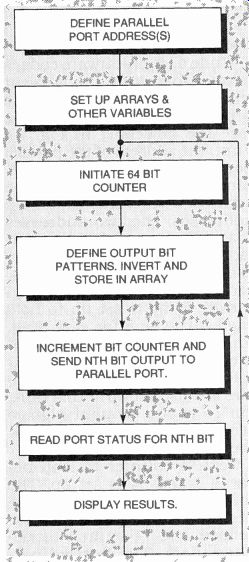
FIG. 3--BASIC PROGRAM FLOW. First, the address of the parallel port that's
going to be used is identified and called ad0 .
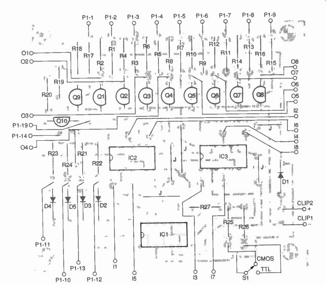
FIG. 4--PARTS-PLACEMENT DIAGRAM. The circuit layout is not critical, so you
can use either the PC board an experimenter's breadboard.
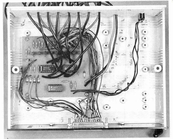
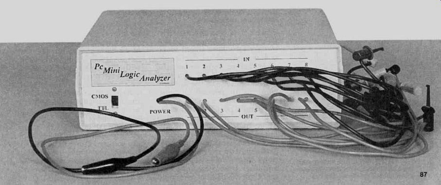
FIG. 5--AUTHOR'S PROTOTYPE. Use micro-clips for the 16 input/output lines,
and insulated mini alligator clips for the power and ground leads. Route the
wires through holes in the enclosure and attach the connectors.
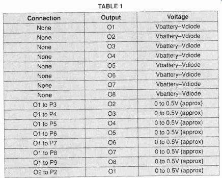
TABLE 1
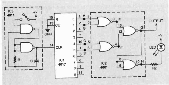
FIG. 6--LOGIC ANALYZER APPLICATION. This self-clocking circuit is supposed
to provide a squarewave output that has one quarter of the input frequency.
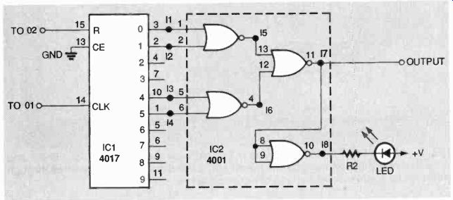
FIG. 7--MONITORING ALL POINTS in the circuit will reveal any problems quickly.
Here's the test circuit with the CD4011B replaced by the analyzer.
Comparator IC1-d compares the signal at its positive input to the reference voltage at its negative input. When the signal is greater than the reference, the comparator's output goes high, and blocking diode D2 is reverse-biased. The high output at pin 14 of the parallel port pulls the parallel port pin 13 in put high. A low signal from the comparator output allows the parallel port pin to sink voltage from pin 14 into the comparator's output through the di- ode. This pulls parallel port pin 13 low when a low signal is provided to the comparator. This arrangement allows signals greater than the 5-volt level of the parallel port to be processed.
The analog switch/comparator block is used four times to accept eight inputs and provide them to the four comparators for input into the PC.
The reference voltages for the comparators are created in the voltage divider consisting of R25, R26, and R27. When switch Si is in its rri. position, the voltage across R27 (provided to the comparators) will be about 2 volts with a 5-volt power supply. With S1 in its cmos position, the voltage across R27 will be about 70% of the power supply voltage. Those voltage levels correspond to the lower limits of valid high logic levels for those logic families. A common ground reference is provided from the power supply through to the PC via the parallel port's pin 19 and clip 2.
LISTING 1
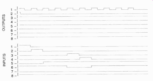
FIG. 8--RESULTING BIT PATTERN. The immediate problem is that the LED does
not light, verified in the bit pattern showing that inputs 17 and 18 are not
switching.
Software
While a lot of software code is devoted to making a convenient interface for the user, the basic program flow is fairly simple (see the flowchart in Fig. 3).
First, the address of the parallel port is identified and called ad0.
Since the parallel port must be addressed with three sequential addresses, the two addresses that follow are defined as ad1 (ad0 +1) and ad2 (ad0 + 2). Because the analyzer has 16 lines, each with a 64-bit sequence, an integer array is set up to hold each bit's value for each line.
The array has maximum dimensions of 16 by 64, or a(16,64). Other necessary variables are also set up at this time.
Pin 14 is also brought high to serve as the pull-up voltage for the parallel port inputs.
Next, a counter to loop between 1 and 64 is set up. The software then makes sure the desired output pattern(s) are defined, and if they aren't, it de fines them. The desired pat terns are inverted (to compensate for the hardware inversion in the interface transistors) and stored in the integer array. Next, the bit counter is incremented and the next bit is sent out to the parallel port. The status of the port is then read and the results are displayed. The soft ware then loops back to the bit counter, and the input/output process continues. There is more to the actual program code, but the basic analyzer operation is captured in just those few steps.
Construction
The circuit layout is not critical, so you can use either the PC board and parts-placement diagram shown in Fig. 4, or follow the schematic diagram and build the circuit on an experimenter's breadboard. For either assembly method, IC sockets are recommended.
Once the circuit is constructed, and before you begin the final wiring, decide on the case style (if any) for enclosing the analyzer. Because 16 wires and test clips extend from the circuit board, it is wise to choose a wire-coding arrangement that will help you easily recognize each input and output lead.
Use No. 20 stranded hookup wire for the 16 input/output leads, connecting one end to the 16 points identified as O1-O8 and 11-18. Again using No. 20 stranded wire, connect a red lead to Clip 1 and a black lead to Clip 2, and also connect switch S1.
Decide if you want to have the parallel port cable connected to the board directly, or if you want to add a DB-25 connector. For the integral cable option, obtain 15 four-foot lengths of No. 22 or 24 stranded wire, or a four-foot length of 15-conductor cable.
Then use those leads to connect the appropriate points from the circuit board to the pins of a male DB-25 plug. If you use a connector, make the appropriate connections from the circuit board to a female DB-25 socket mounted on the back of the case with wire cut to the size of the enclosure.
The last step is to attach connection devices to the 16 input/ output lines and power leads.
Use micro-clips for the 16 input/ output lines, and insulated mini alligator clips for the power and ground leads. Route the wires through holes in the enclosure and attach the connectors. Complete the assembly by mounting the circuit board in the enclosure and mounting S1. Figure 5 shows the author's prototype unit.
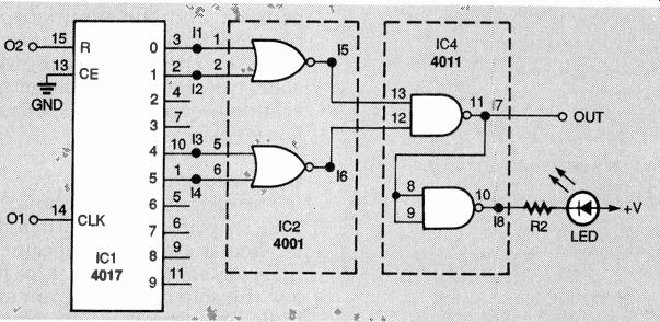
FIG. 9--A NAND FUNCTION will produce a low logic level when the two inputs
are high, and produce a high logic level otherwise. Here's the revised circuit.
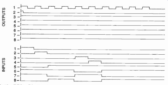
FIG. 10--RESULTANT BIT PATTERN of the circuit in Fig. 9.
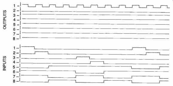
FIG. 11--THE I7 AND 18 WAVEFORMS would both be symmetrical if they ended after
the eighth clock pulse. Routing the ninth output of IC1 to the reset pin will
do this.
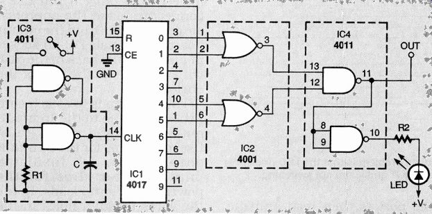
FIG. 12--THIS FINAL CIRCUIT configuration meets all of the original requirements;
the output is the input divided by 4, it is symmetrical, and the LED lights.
Checkout
To test the analyzer, you'll need a 9-volt battery, a volt meter, and a few jumpers. First make sure that there is no continuity between the board and the eight output leads 01-08.
Then connect the power terminals to the 9-volt battery (red to + , black to- ). The voltage between each of the output leads and ground should be the battery voltage less the voltage drop across diode DI. For example, if your battery terminal voltage is 8.9 volts, the voltage at 01 should be about 8.6 volts. The actual voltage is not critical, be cause the drop across DI and the individual transistors will vary slightly depending on the actual devices installed.
Next, connect 01 to P1 pin 3; 02 should now read between 0 and about 0.5 volt. Connect 01 to P1 pins 4 through 9 in turn, reading the outputs (03 through 08 respectively). Finally, connect 02 to P1 pin 2 and read the output at 01. This en tire procedure is summarized in Table 1.
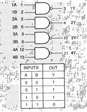
FIG. 13--TO USE THE ANALYZER to check a CD4011B NAND gate, begin with the
truth table and functional diagram.
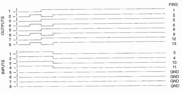
FIG. 14-THE TRUTH TABLE of the CD4011B is implemented in this hit pattern.
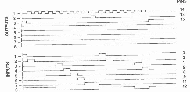
FIG. 15--BIT SCAN for the CD4017B CMOS decade counter/divider.
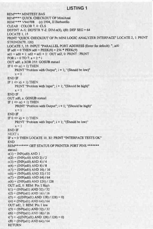
To check the interface input circuits and parallel port connections, use the program MATEST.BAS shown in Listing
1. (All of the software for this analyzer project will be made available on the Gernsback BBS, 516-293-2283, v.32, v.42bis, as a file called MINI ANAL.ZIP.) Extract the program MATEST.EXE from the zipped file or type it in by hand and run it from QBasic. Connect each numbered output to its corresponding input (01 to II, 02 to 12, etc.). Connect the power leads to a 9-volt battery, and connect the analyzer output to your computer's parallel port.
Place S1 in the CMOS position.
The program will use the outputs to create a logic 1 and then logic 0 for each of the eight in puts. It will read the inputs to determine if they were processed correctly. When you execute the program, it will ask you for the parallel port address. Press ENTER if you're using LPT1 at the standard address of 888.
Otherwise, type in the decimal address of the parallel port and press ENTER. The program will then test all inputs and outputs, and give you the results.
You will either get a message "Interface Tests OK," or one or more messages indicating which inputs or outputs did not perform as they should.
Logic analyzer
To use the unit as a logic analyzer, begin with the following sample problem: Assume Fig. 6 is a self-clocking circuit that you designed to provide a squarewave output that is one quarter of the input frequency.
The clock can be disabled with an external switch, and the LED should turn on with the rising edge of the clock. If wired as shown, the circuit does not operate properly. Most notably, the LED doesn't flash.
Before testing the circuit, IC3, a simple squarewave generator, must be replaced with one of the analyzer's outputs. If IC3 were left in the circuit, there would be no way to synchronize it with the analyzer, and the display would drift, resembling an oscilloscope trace without proper sync. The IC3 oscillator is therefore simulated by programming an analyzer output to produce a squarewave.
Although IC1 is a divide-by-ten counter, the analyzer has a 64-bit pattern that is not evenly divisible by ten. Again to avoid pattern drifting, a second output must be programmed to re set IC1 after ten clock pulses.
Finally, the correct monitoring points must be determined. For the best understanding of circuit operation, all possible points (A through H) should be monitored. The resulting test circuit is shown in Fig. 7.
The bit pattern obtained is shown in Fig. 8. The fault with the circuit was that the LED would not light. The problem is verified in the bit pattern showing that inputs 17 and 18 are not switching. However, the outputs of IC1 are performing as expected, and the outputs of the first two NOR gates (15 and 16) are also valid. Re-examining the circuit with the help of the analyzer reveals the fault: At least one of the inputs (15 and 16) to the third NOR gate (I7) is always logic high. That makes the output always logic low. The circuit really needs a NAND function to produce a low logic level when the two inputs are high, and to produce a high logic level at other times. The solution is to change the circuit to incorporate a NAND gate. The revised circuit is shown in Fig. 9, and the resultant bit pattern is shown in Fig. 10.
Replacing the NOR gate with a NAND gate has provided the desired signals at 17 and 18. (The fourth NOR gate was also re placed with a NAND gate arbitrarily--either gate can serve as an effective inverter/current sink for the LED). By looking at the new bit pattern, you might notice another problem. The circuit is dividing by four, but it is not producing a symmetrical squarewave. The pattern is symmetrical through the eighth positive clock pulse (01), but then stays low for the remaining two clock pulses. In viewing the bit pattern this will be immediately obvious, and it is much better than attempting to watch the LED while determining what's wrong.
FIG. 16--THIS SIMPLE JIG makes connections to the IC pins easy.
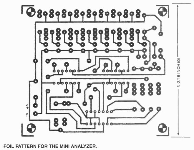
------- FOIL PATTERN FOR THE MINI ANALYZER.
A look at the 17 and 18 wave forms shows how to solve the problem. They would both be symmetrical if they ended after the eighth clock pulse. This can be accomplished by routing the ninth output of IC1 (called output 8 because the first one is called output 0) to the reset pin.
This will create a divide-by-8 counter instead of a divide-by-10, and it will generate the bit pattern in Fig. 11. Notice that the 02 reset pulse has been removed-it is no longer needed because a hardware reset has been incorporated. Because the circuit divides by 8, and the 64-bit pattern is divisible by 8, the bit pattern is stable, or synchronized. The final circuit con figuration is shown in Fig. 12. It meets all of the original requirements in that the output is the input divided by 4, it is sym metrical, and the LED lights on the rising edge of the clock.
IC checker
This example will expand on the last example. The analyzer will check for proper operation of the CD4011B NAND gate. Be gin with the truth table and functional diagram of the 4011 shown in Fig. 13. Any combination of inputs other than both logic high will produce a "1" output; a logic high to both inputs of any of the four NAND gates will cause that gate to produce a "0" output. lb test the IC, you must program the four possible input bit patterns for each gate and view the corresponding outputs. If each gate stays high except when both inputs are high, the IC is functioning properly.
The truth table is implemented in the bit pattern of Fig. 14. Note that the pin connections are indicated to the right of the traces. Inputs 5 through 8 are grounded to avoid stray pickup. Ground any unused in puts to avoid stray signal pick up through the high off-impedance inputs of the CD4066 switches. Alternately, you can attach a pull-down (terminating) resistor to each in put. Any resistor value of 10,000 ohms or more will work fine and not load the source circuitry.
Instead of a single bit, a group of bits (five in this case) will be used for each state. Each set of inputs to the 4011 (01 and 02, 03 and 04, 05 and 06, and 07 and 08) have the same pattern.
The first five bits of each set are low. Then the second five bits are low on the first input and high on the second. Then the pattern flips, with the next five bits high on the first input and low on the second. Finally, the bit pattern shifts to both inputs high. In each instance, the expected IC output pattern (II, 12, 13 and 14) show a high input until the inputs shift to both high. Then the IC output goes low A bit scan for the CD4017B CMOS decade counter/divider is shown in Fig. 15. The input bit pattern from a reference book was used directly, except that IC outputs 2, 3, and 4 were not sensed (because the IC has 11 outputs, and the analyzer has only eight). This approach checks all the functions of the 4017, including reset, clocking, clock enabling, and carry out. A second scan could be performed to sense the previously un checked outputs instead of IC outputs 6, 7, and 8.
Most digital ICs can be tested in a similar process. That is, you must determine the necessary inputs to exercise all functions of the IC, program those inputs, determine where to ob serve the outputs and what those outputs should be. Then you can compare the results.
To make a simple jig for this purpose, you can use a general purpose IC PC Board (Radio Shack Part No. 276-159) and a 20-pin IC socket. Solder the socket in place, and solder a sol id wire loop on each of the in put/output pads. The jig is shown in Fig. 16.