by RICHARD L. ROANE
Control eight channels of 120-volt AC with a 68705.
HAVE YOU EVER WANTED TO VARY the power delivered to a 120-volt AC load under software control? In this project a 68705 microcontroller will do just that. Specifically, it can control eight discrete power Triacs, each of which delivers power in 32 smoothly graduated steps ranging from 0 to 97% of full power.
The value delivered to one channel is independent of the value delivered to any other channel.
Loads can include light displays, universal motors, heaters, and other appliances.
In this circuit, the power level is set by software, not a potentiometer. The software includes a basic set of routines for processing interrupts and setting the power level. The software also includes five test and demonstration routines for putting the circuit through its paces.
Moreover, there's plenty of room to add your own routines to the 68705's built-in EPROM. An easy-to-build single-sided circuit board makes assembly easy.
The basic circuit is simple, yet versatile enough to accept inputs from on-board DIP switches; alternatively, the in puts can be driven from a microcomputer bus or parallel port, or a stand-alone device with TTL-compatible outputs. There are 12 input bits to set modes and specify values.
Circuit design
The circuit, shown in Fig. 1, consists of a power supply, AC line synchronizer, 'Iliac output control, input circuitry, and support devices.
The power supply is a conventional 5-volt circuit built around a 7805 regulator (IC3) and several other components (transformer T1, bridge BR1, and C1-C4). The AC line synchronizer consists of an optocoupler (IC2), a current-limiting resistor (R1), and a bias resistor (R2). The power controller generates variable power levels with phase-control techniques. When using a Iliac to control a load, the power delivered can be varied by triggering the Triac after the start of an AC half-cycle.
For example, by triggering the Iliac shortly after the start of a half-cycle, the load will receive almost full power. Triggering in the middle of a half-cycle will supply the load with half power and triggering close to the end of a half-cycle will result in the load receiving little power.
In this project the controller is synchronized to AC power-line zero crossings, which occur at a rate of 120 times per second.
The microprocessor's internal timer then divides the interval between crossings into 32 steps, thus delivering gradually increasing amounts of power to the load.
The output of the optocoupler is a negative-going pulse that drives the microcontroller's interrupt input directly at a rate of 120 hertz. Each time IC1 receives an interrupt, it recalculates the time to generate Triac trigger pulses on Port B of IC1.
Each bit of Port B is connected to a 'Iliac control circuit; since they're all identical, only Port 7 will be described in detail. Port B7 of IC1 drives transistor Q1 via resistor R4. (Q1 is required because the 68705 can't sink enough current to trigger Iliac-driver IC4 directly.) When it's time to turn on 'Iliac TR1, the microcontroller delivers a 10-microsecond negative-going pulse to port PB7. That pulse briefly enables the transistor, which causes current flow through the LED inside IC4. Although a Motorola MCP3011 Iliac driver was used in this design, any similar device could be used, as long as it doesn't have an internal zero-crossing detector. That type of driver allows only two modes of operation: full on and full off.
The Triac driver's LED then triggers the photon-coupled ili ac within the IC, which in turn triggers TR1 and delivers power to the external load. Resistor R5 provides current limiting for IC4, and R6 and C7 form a snubber network to filter line transients that could cause the Iliac to trigger falsely.
The hot side of the power line connects to the MT1 terminal of all the power Triacs (TR1-TR8).
The specified lilacs are rated for 4 amperes at 200 volts. They are isolated-tab versions, and were selected because heatsinking is mandatory. With the specified Triacs, the maximum load is 100 watts per output. Larger loads can be handled by substituting triacs with higher current ratings. Be sure to use proper heatsink and isolation techniques.
Input circuit
The input circuit consists of Ports A and C of the micro-controller, along with two banks each of DIP switches (S1 and S2), SIP resistors (RN1 and RN2), four sets of 0.1 inch header jumpers (P1-P4) for mode selection, a 14-pin header (P5) connected to Port A, and a four-pin header (P6) for input selection.
The P1-P4 jumpers allow both the common resistor legs and the common switch poles to be tied to either ground or +5-volts DC, or to be disconnected from the circuit entirely. If programmed as inputs, the ports should not be left floating be cause this might cause erratic operation. Connector P6 allows an external device (e.g., a computer) to drive the controller's inputs.
The 68705P3 requires a few support components. Crystal XTAL1 runs at a frequency of 3.58 megahertz, which should not be altered. Capacitor C5 loads the oscillator to keep it at the correct frequency, and capacitor C6 keeps the reset pin low for an instant, thereby giving the 68705 time to stabilize after power up. Momentary switch S3 provides for resetting the circuit. Although unused in the prototype, an external connection is provided to the microcontroller's RESET input, which could allow an external device to reset the circuit when desired.
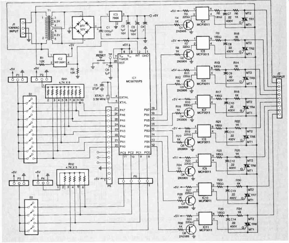
FIG. 1--COMPLETE SCHEMATIC OF THE 68705-based power controller. The controller
reads switch values from Ports A and C, and delivers software-controlled
120-volt AC power to Port B.
------
PARTS LIST
All resistors are 1/4-watt, 5%, unless otherwise noted.
R1-12,000 ohms, 1 watt
R2-10,000 ohms
R3, R7, R11, R15, R19, R23, R27, R31-220 ohms
R4, R6, R8, R10, R12, R14, R16, R18, R20, R22, R24, R26, R28, R30, R32, R34-1000 ohms
R5, R9, R13, R17, R21, R25, R29, R33-180 ohms
RN1-4700 ohms x 9 resistor network, common terminal
RN2-4700 ohms x 5 resistor network, common terminal
Capacitors:
C1-1000 µF, 16V, radial electrolytic
C2-1 µF 16V, tantalum
C3-10 uF, 16V, radial electrolytic
C4, C15 0.1 uF, monolithic
C5-27 pF, ceramic
C6-1 uF, 16V, radial electrolytic
C7-C14--0.22 uF, 400V, poly film
Semiconductors:
IC1-MC68705P3 microcontroller
IC2-H11AA1
AC optocoupler:
IC3-MC7805CT 5-volt regulator
IC4-1C11-MCP3011 Triac driver
Q1-Q8--2N3906 NPN transistor
TR1--TR8-02004L3 Triac, 200V, 4A, isolated tab
BR1--Bridge rectifier, 50V, 1A, DIP
Other components:
J1-3-terminal AC power connector
J2-9-terminal AC power connector
P1-P4-3-pin single-row 0.1 inch male header
P5-14-pin single-row 0.1 inch male header
P6-4-pin single-row 0.1 inch male header
S1-8-position DIP switch
S2-4-position DIP switch
S3-SPST momentary pushbutton switch
T1-Transformer, 120V primary, dual 6.3V secondaries (Digi-key T101-ND or equiv.)
XTAL1-3.579545 MHz crystal, HC-18
Miscellaneous:
Shorting jumpers for P1-P4, heatsink for TR1-TR8, PC board, solder, wire, etc.
Note: The following items are available from Richard L. Roane, Route 601, Cologne, VA 23037:
Source code listing and programmed MC68705P3-$24.95 postpaid VA residents must add appropriate sales tax.
-------
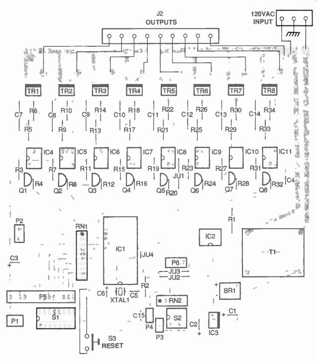
FIG. 2-MOUNT ALL COMPONENTS AS SHOWN HERE. Note that four jumpers mount
on the component side of the board.
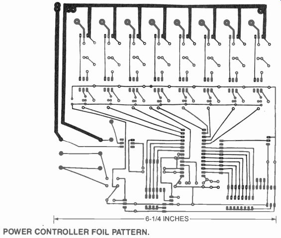
-------------- POWER CONTROLLER FOIL PATTERN.
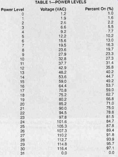
TABLE 1--POWER LEVELS
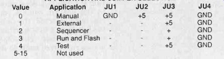
TABLE 2--APPLICATION AND JUMPER SELECTION
TABLE 3--MANUAL MODE POWER LEVELS
Software design The complete listing of the software is available from the author, as detailed in the Parts List. It is also available on the Gernsback BBS (516-293-2283, v.32, v.42bis); look for file POWCON.ASM. An overview of the major routines follows:
The interrupt routine sets up the microcontroller's internal timer to produce 31 timer interrupts per half-cycle. Together with the full-off value, those interrupts provide the 32 power levels. Table 1 lists power level, corresponding voltage, and percentage of full on. A power value of 0 represents the lowest on voltage, 30 represents the highest, and anything greater than 30 represents a voltage of 0.0.
Eight bytes of RAM (PWRCO-PWRC7) function as control bytes, each corresponding to a Port B output bit. Each byte stores one item of power level data (as shown in column 1 of Table 1). To see how a value in a control byte is translated into an output voltage, follow this example.
Suppose that an application calls for a power level of 16 at Output 3, and a level of 30 at Output 7. In that case simply store values of 16 and 30 in control bytes PWRC3 and PWRC7, respectively. The outputs will immediately and simultaneously reflect these levels. Note that although the desired voltages were specified in decimal form, you must store the corresponding hexadecimal value in the output-control byte.
A "hole" was left in the micro-controller's EPROM (addresses $80-$5FF) for application pro grams. The five demonstration routines discussed earlier occupy those addresses. You are free to create your own applications, but leave the addresses outside that range alone. Ad dresses below $80 are reserved for constant and variable storage; addresses above $5FF contain the reset and interrupt routines. All 68705 registers, except for the timer, are avail able for use by application routines.
-------
ASSEMBLER VARIATIONS
In developing the software for this article, the intention was to provide a single source file that would assemble correctly under three assemblers: the TECI 6805 Assembler, Motorola's 6805 Assembler, and Motorola's Freeware Assembler. In the course of testing, a bug was discovered in the Freeware assembler. After encountering an instruction that uses direct addressing on page zero of memory, the assembler starts generating garbage. Both of the other assemblers force extended addressing, thus avoiding the problem. The only point in the code where this is a problem is in the jump table, where there is the instruction:
JMAN: JMP MAN
By changing that instruction as follows, the problem can be avoided:
JMAN: BRA MAN
Branching, rather than jumping, works because the target routine is with in 128 bytes of the jump table.
--------
Construction
Assembly is straightforward.
Figure 2 shows the parts layout on the single-sided circuit board. Load the board by inserting lowest- to highest-profile components. Make sure that you observe polarities of all semiconductors, SIP resistors, and electrolytic capacitors.
For the prototype, four Triacs were mounted each to two 90° aluminum heatsinks. The AC power input was brought to one heavy-duty, three-terminal connector, and the eight mac outputs plus AC common were brought to a separate nine-terminal connector.
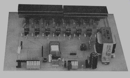
The circuit board has 120-volt AC signals on it, so check and double-check your work before plugging in and testing the project. Figure 3 is a photo of the author's prototype.
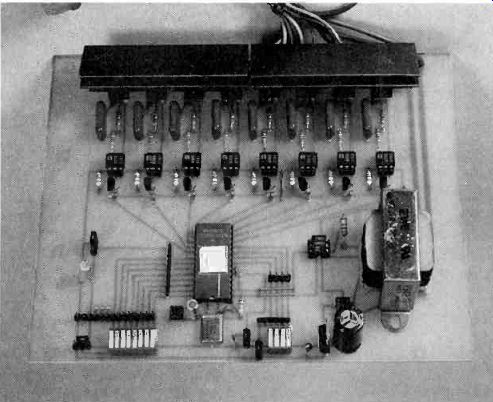
FIG. 3--COMPLETED UNIT. The circuit board has 120-volt AC signals on it,
so check and double-check your work before plugging in and testing.
Built-in applications
On power up, a selection routine reads Port C and selects the corresponding application.
Note that following power-up, Port C can be used for other purposes. Table 2 lists Port C values, along with the corresponding routines and PC-board jumper settings. In general, if no host is connected and Port A will input data from S1, set the jumpers as shown for application 0 (manual). Also note that in the design, once a routine has been selected, the only way to change to a new routine is to reset the system. The following is description of each in detail.
Manual
The software scans Port A waiting for a bit to go low. When that occurs, the microcontroller loads power-level data from Port C and stores it in the power-control byte specified by the value in Port A. For example, placing 05 on Port C and bringing PA2 low will set output 2 to power level 8.
Because Port C has only four in put bits, it can only specify 16 power values (2^4= 16). Thus a look-up table (shown in Table 3) spreads the 16 specifiable values across the entire 32-value range.
-------------
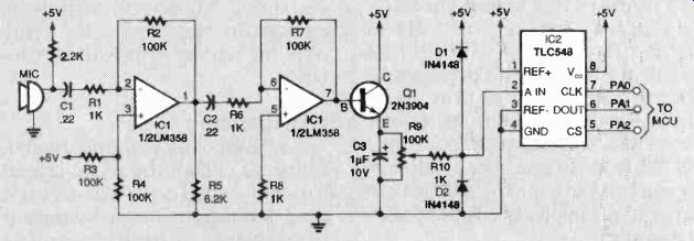
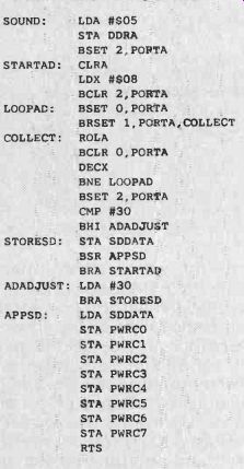
SOUND INPUT
The accompanying schematic shows a simple circuit for letting an audio sound source control the power-controller output. The circuit accepts input from a standard crystal microphone, and amplifies the signal using two op-amp stages. The signal then passes through an emitter-follower circuit that drives a TLC548 kD converter. Potentiometer R10 functions as a sensitivity control.
The software, presented below, simply clocks the kD converter eight times, accumulates the result, then stores it in all eight output registers, from where they are applied to the Triacs in the usual manner. To use the routine, you'll have to declare the variable SDDATA, add the routine itself to the jump table, and add a new S1 switch setting to the application- selection power-up routine.
SOUND MODE ROUTINE
------------
Sequence
This routine demonstrates the controller's ability to power light displays. It turns on the first output, waits, then turns it off. It then repeats that action for output 2, and so on. After output 7 toggles, the software then repeats the cycle.
Run and flash--This is a variation of the sequencer application. It sequences the outputs for five cycles, then flashes all eight three times and repeats the cycle.
Test--The test application tests the controller. The routine steps the outputs through all 32 power levels, pausing one second between each.
External--Here's where things get interesting. This routine allows an external source, such as an intelligent I/O module or a computer, to control power levels. 'lb get into this mode, set switch S2 to a value of 2, install the correct jumpers, then reset the circuit. From then on, input Port CO functions as a strobe that causes the microcontroller to read the value on Port A and perform the proper function.
When cop goes low, the micro controller reads Port A. It then splits the value into a 5-bit power specification (PAO-PA4), and a 3-bit output port (PA5-PA7).
The 5-bit power specification al lows 1 of 32 values; the 3-bit output port allows 1 of 8 ports.
For example, assume you place the value $57 on Port A and strobe Pco low In binary,
$57 =0101 0111. Taking the up per three bits yields 010, or 2.
Taking the lower 5 bits yields 10111, or 23. Thus the controller will set output 2 to level 23.
Summing up
As you can see, both hard ware and software are simple and suitable for being customized. For example, you could connect the output of an A/D converter to Port A, then vary power levels based on some analog quantity.
When creating your own routines, be sure to include it in both the power-on Select routine and the Jump Table. That way the controller will know where to find it.
adapted from: Electronics Now--Electronics Experimenter's Handbook 1996