Double the frequency of any sinewave from 10 Hz to more than 50 MHz.
by STEVEN D. SWIFT
HOW OFTEN HAVE YOU WISHED THAT your signal generator would generate a higher frequency? The small module described in this article doubles the frequency of any sinewave input, providing outputs from 10 hertz up to and beyond 50 megahertz.
It measures less than 2 x 3.5-inches, and consumes about one-third of a watt. It can be permanently installed in almost any signal generator or used as an outboard module.
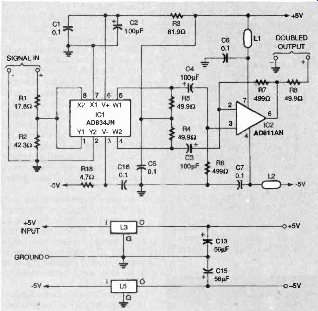
FIG. 1--SCHEMATIC OF THE FREQUENCY DOUBLER. An Analog Devices AD834 wideband,
four-quadrant multiplier (IC1) provides wideband analog multiplication of two
input signals.
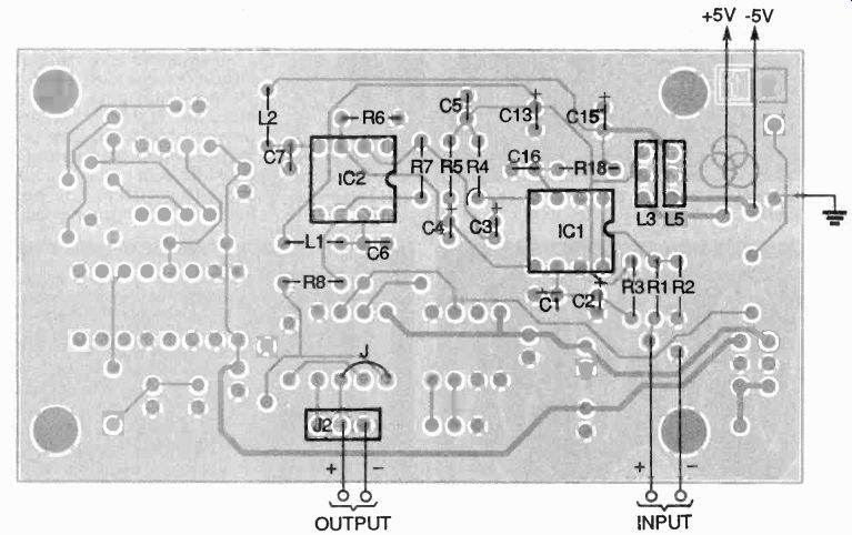
FIG. 2--PARTS-PLACEMENT DIAGRAM. Square pads are on pin 1 of all ICs and on
the positive leads of all polarized capacitors.
Theory of operation
A schematic of the frequency doubler module is shown in Fig. 1. The core of the module is ICI, an Analog Devices AD834 wide-band four-quadrant multiplier.
This IC provides wideband analog multiplication of two input signals, regardless of their polarity. In this circuit both X and Y inputs are tied together to provide a squaring function.
The operation of IC1 is best understood with the aid of simple mathematics. If the input is assumed to be a normalized (amplitude of 1) sinewave of frequency f, then the input can be written as:
Input = sin(2 pi t) where
pi = 3.14159...
f = frequency t = time
The AD834 performs the following function:
XY = sin(2nt) x sin(at)
= (sin(2nt))2
A fundamental trigonometric identity gives:
(sin(2nt))2 = (1- cos(2(2nt)))/2
= (1- cos(2n2f))/2
The last term shows a DC off set as well as a cosine term with twice the frequency as the in put. This performs the frequency doubling function. The shift from the original input, cosine term exhibits a 90° phase but phase is of no concern in this circuit. Note, however, that the amplitude is cut in half.
Since the AD834 provides differential current-mode outputs, load resistors R4 and R5, gain resistors R6 and R7, and IC2 are added to convert the signal to an amplified and buffered single-ended output. The AD8I 1 wideband current-mode feed back amplifier (IC2) is configured as a differential amplifier.
Capacitors C3 and C4 remove the DC offset from the output.
Resistor R8 provides a nominal 50-ohm output impedance, and R1 and R2 attenuate the input signal and provide a low-impedance source to ICI.
Inductors L1, L2, L3, and L5 and capacitors C5, C6, C7, C13, and C15 perform high-frequency filtering and decoupling. Resistors R3 and R18 and capacitors C1, C2, and C16 provide decoupling and biasing for IC1.
The circuit requires a + 5-volt supply at about 30 milliamperes and-5 volts at about 40 milli amperes. Higher voltages, up to ± 9 volts, can be used if the bypass capacitor voltage ratings are increased. Higher voltages provide higher bandwidths with higher power dissipation.
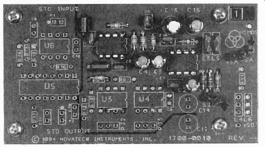
FIG. 3--THE COMPLETED BOARD. The locations for extra components are for other
board applications.
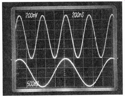
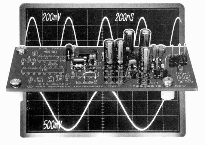
FIG. 4-- INPUT AND OUTPUT. The top trace is the output of the doubler with
a 1-megahertz, 1.5-volt peak-peak input signal, and the bottom trace is the
input signal.
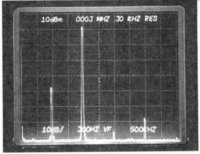
FIG. 5--FREQUENCY SPECTRUM of the output signal in Fig. 4.
The fundamental frequency is about 40 dB down from the doubled frequency.
====
PARTS LIST:
All resistors are 1/2-watt, 1%, metal film, unless noted.
R1--17.8 ohms
R2-42.3 ohms
R3--61.3 ohms
R4, R5, R8--49.9 ohms
R6, R7--499 ohms
R18--4.7 ohms, 1/4-watt
Capacitors:
C1, C5, C7, C16--0.1 uF, ceramic
C2-C4--100 uF, 6.3 volts, high-frequency aluminum electrolytic
C13, C15--56 uF, 16 volts, high-frequency aluminum electrolytic
Semiconductors:
IC1-AD834JN wideband multiplier (Analog Devices)
IC2-AD811AN current mode amp (Analog Devices)
Other components:
L1, L2--Leaded EMI bead (Panasonic EXC-ELSA35, Digi-Key PC820BK-ND)
L3, L5--3-terminal EMI filter (Panasonic EXC-IEMT103DT, Digi Key 9809CT-ND)
L4--not used
Miscellaneous:
PC board, wire jumpers, seven 0.J25-inch square posts (if desired), solder.
Note: The following items are available from Novatech Instruments, Inc., 1530 Eastlake Ave. East, Suite 303, Seattle, WA 98102:
Complete kit of all parts (Model DOUB-1, includes PC board and documentation)--$50.00
Please add $5 shipping / handling for US and Canada. $10 overseas. Add $10 for COD orders. Washington State residents muss add 8.2% sales tax.
Check or money order only.
====
Construction
Because IC1 and IC2 are high-frequency components, you must be extremely careful to prevent high-frequency oscillations if you build the circuit on a breadboard. It is preferable to use a PC board. A foil pattern is provided here. Keep all wires short and place the bypass capacitors as close to IC1 and IC2 as possible. A solid ground plane on the component side of the PC board is recommended, and IC sockets are discouraged.
If you must use sockets, use machined-pin, open-frame sockets only.
As can be seen from the parts-placement diagram, the board has locations for extra components not related to the doubling function discussed in this article. The additional features were included to allow the board to be used with other Novatech synthesizers.
The parts-placement diagram is shown in Fig. 2. Install all the components as shown, taking care to observe polarity on di odes and capacitors. Square pin 1 of all ICs and the positive leads of all polarized capacitors.
All resistors specified for this circuit (except R18) are 1/8-watt, 1% metal-film types. Their small size and tight tolerance improves high-frequency performance and circuit matching. If resistors other than metal-film are substituted, the performance of the frequency doubler will be degraded. In particular, its distortion will increase, and its bandwidth will decrease.
As mentioned before, C3 and C4 provide DC blocking. The values specified allow operation down to about 10 hertz. If you intend to use this circuit exclusively above 5 kilohertz, better high-frequency performance can be obtained by substituting 0.1 µF ceramic capacitors. The extra capacitors are included with the kit for this purpose.
Figure 3 shows the board.
Checkout
Verify that all components are installed properly and that there are no solder bridges. Apply power to the board as indicated in Fig. 2 (plus and minus 5 volts DC, both ± 0.25 volt).
Also connect a function generator set to approximately 1 volt RMS to the signal input as shown. Connect an oscilloscope or frequency counter to the output pin (the center pin of J2).
Observe that the output is double the frequency of the in put signal as the input is varied.
The typical 3 dB point of the doubler is greater than 30 megahertz at the output.
You can adjust the input to vary the output, but with an input above about 1.5 volts RMS, the output might be clipped.
The top trace in Fig. 4 is the output of the doubler with a 1-megahertz, 1.5-volt peak-to-peak input signal, shown at 200 millivolts per division. The bottom trace is the input signal at 500 millivolts per division. Figure 5 shows the frequency spectrum of the output signal in Fig. 4. The fundamental frequency is about 40 dB down from the doubled frequency, the second harmonic is more than 65 dB down, and the third is about 60 dB down. This fundamental frequency feedthrough increases to about- 20 dB below the carrier as the output is increased to 50 megahertz.
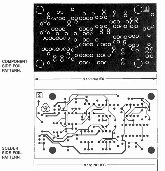
-------COMPONENT SIDE FOIL PATTERN.
-------SOLDER SIDE FOIL PATTERN.
adapted from: Electronics Now--Electronics Experimenter's Handbook 1996