1. SMALL SIGNAL AND PRE-AMPLIFIERS
Preamplifiers are used to convert low level signals into higher level signals with low output impedances. The primary design considerations for preamplifiers are input impedance, signal gain, equalization, noise performance and distortion. It is now possible to buy integrated circuits that will perform virtually all common preamplifier functions. Only rarely, (and with a lot of skill), will one be able to improve upon a monolithic 'best' solution with a discreet component design. However, it is necessary to fully understand the operation of the IC if optimum results are to be obtained.
The Op Amp Building Block
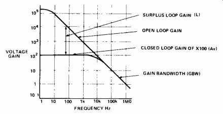
Fig.1. Typical frequency response for the 741 op amp.
Most IC preamplifiers operate as op amps. They have a single or differential input, a low impedance output and a large frequency dependent voltage gain, (Fig.1). Note that the open loop voltage gain rolls off at -6 dB per octave. By applying feedback around the op amp (closed loop), the gain is stabilized and is held constant by the resistor ratio until the device runs out of bandwidth. The difference between the open and closed loop gain is known as the surplus loop gain.
This surplus loop gain is the negative feedback that is used to iron out non-linearities in the op amp. As the size of the surplus loop gain decreases with increasing frequency, the distortion and output impedance increase. Fig.2 compares the performance of inverting versus non-inverting configurations.
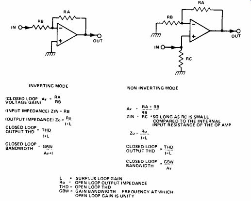
Fig. 2. A comparison of the performance of inverting versus
non-inverting configurations.
Note that for unity gain the non-inverting mode has twice the closed loop bandwidth of the inverting mode. Also note that the output impedance rises as the surplus loop gain decreases.
This can cause a sharp increase in distortion when the op amp is driving a low impedance load at high frequency.
Design Example
Q. Design an amplifier with a gain of 60 dB, a closed loop bandwidth of at least 20 kHz and input impedance of 10 k.
A. First, try the inverting mode as shown in Fig.2.
Zin = 10 k = RB.
Av = 60 dB = X1000 = RA RB
Therefore, RA = 10 k x 1000 = 10 M
If we use a 741 then the input offset voltage will be multiplied by the closed loop gain. The offset is typically ± 1 to 5 mV.
Therefore, the output offset will be ± 1 to 5 V! It is possible to null out the input offset (Fig.3a) with a preset. This circuit will not be very satisfactory.
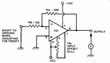
Fig.3a. The input offset can be nulled with a preset.
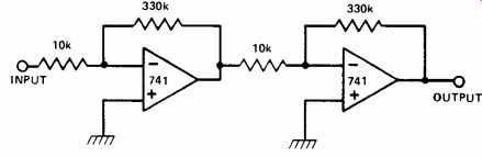
Fig.3b. A cheaper way to achieve higher gain at, say, 20 kHz
without
Its DC output offset will probably drift with temperature and time. If stable high DC gains are required then a 741 should not be used. A high performance instrument op amp should be selected in its place. Another problem in using the 741 is its 1 MHz gain bandwidth product. A closed loop gain of 60 dB will result in a closed loop bandwidth of 1 kHz, and not the 20 kHz needed. An op amp capable of giving 60 dB of gain at 20 kHz would need a gain bandwidth product of 20 MHz.
Although there are some op amps with this performance, they are generally difficult to stabilize and are relatively expensive. A cheap solution is to use two 741s, both with gains of 30 dB (x 33), (Fig.3b). The 741 has a bandwidth of 30 kHz at 330k a closed loop gain of 30 dB. The DC offset still remains a problem, but it could be removed with a nulling preset on the first op amp. However, if the amplifier is to be used for audio then a DC response is not needed and so AC coupling can be used to reduce the final DC offset, Fig.3c. Yet another problem still exists. With the input short circuited the circuit would probably produce about 10 mV of noise at its output.
The subject of noise will be dealt with later; suffice it to say that the 741 is not a low noise device. Low noise operation can be obtained by using one of the low noise op amps that are now available.
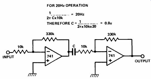
Fig.3c. AC coupling can be used to produce the final offset
in audio applications.
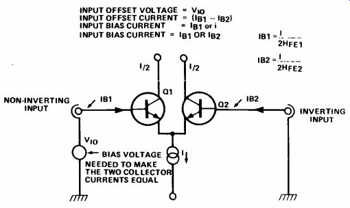
Fig. 4. Typical differential opamp input.
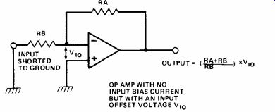
Fig. 5. The effect of V10.
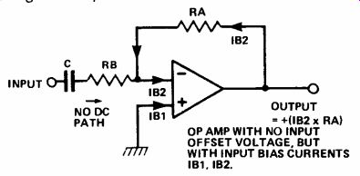
Fig.6. The effect of IB.
Input Offset Voltage and Bias Current
When using op amps as DC amplifiers there are several sources of errors, Fig.4. The input to an op amp is usually an NPN differential pair. To make the device operate, a base current must be supplied (input bias current). Also, to balance the op amp the current through both transistors must be equal. The transistor pair is 'matched' for parameters such as Hfe and Vbe versus ICE. However, small differences are caused by the manufacturing process, resulting in the base currents being different (input offset current) and also the base -emitter voltage parameter input offset voltage). The input offset voltage is multiplied by the closed loop DC gain of the op amp (Fig.5) and the input bias current sets up a DC offset across any resistors it flows through (Fig.6). Typical parameters for the 741 op amp are; 2 mV (V10), 80 nA (IB) and 20 nA (1131 -I132). These parameters vary from device to device and from manufacturer to manufacturer. The purpose of successful design is to produce circuits that are insensitive to these variations. Generally, for audio designs, the DC offsets may be eliminated by AC coupling and other methods (Fig.7). Note that the DC output offset may be reduced by inserting a resistor from the non-inverting input to ground. Without that resistor the DC offset may well have been ± 26 mV (1B2 x RA) as opposed to ± 6.6 mV ((I131-1132)xRA).
A DC voltage on the output would generate a disturbing crackle when the level pot is adjusted.
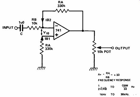
Fig.7. An amplifier with a gain of 30 dB.
Voltage Swing, Power, & Bandwidth
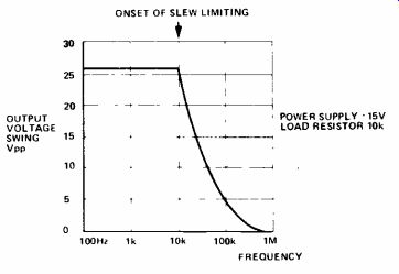
Fig. 8. Typical power bandwidth for a 741 op amp.
The voltage swing at the output of an op amp is limited in many ways, Fig. 8. Most op amps can only swing within a few volts of either supply rail. Also, the speed at which the output voltage can move is limited by the slew rate of the device, which is typically 0V5 per microsecond for a 741. This is the limiting factor in designing amplifiers for high level large signal voltages.
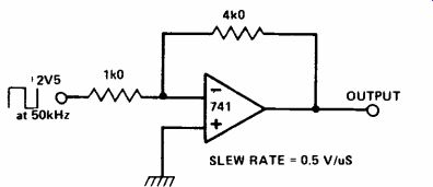
Fig. 9. The difference in slew rate between a 741 and a TL081.
Design Example
Q. Design an amplifier with a gain of 4 to amplify a 50 kHz 5 V squarewave.
A. First try a 741, Fig.9. The required output swing is ± 10 V. The 741 can only move at 0V5/uS and so in the half period of the square wave, it can only move 5 V. If the 741 is replaced with a faster device, the TL081 (13 V/uS) then a `square' wave is produced. The TL081 would take approximately 1.5 uS to travel the 20 V distance, thus generating a rise and fall time of 1.5 uS. Note, that if the resistors were increased in value to say 250k and IMO, then the squarewave output would ring. This is because the feedback would have to charge-up the stray capacitance at the inverting input, thus generating a lag between the output and the feedback, which in turn would generate an overshoot.
Noise
Noise is always a problem in electronics. The presence of noise degrades the quality of the signal we are interested in.
Every time we amplify, process, transmit, record or replay a signal, noise is introduced thus worsening the signal to noise ratio. Some common signal to noise ratios are shown below.
Telephone 20 to 40 dB
Cheap cassette player 30 dB
Good tape recorder 60 dB
Professional studio equipment 80 dB
The calculations of noise produced by electronics is complex, but with a few short cuts it is possible to get some useable calculations.
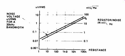
Fig. 10. Thermal noise generated by a resistor.
All resistors generate noise due to thermal agitation (Fig.10). Noise is also generated when a voltage is applied to them. Manufacturers generally express this latter noise in uV/V typically 0.1 uV/V for metal film devices. For most purposes resistor noise is not a dominating noise source although low level amplifiers perform slightly better with metal film devices. Keeping the resistor values low, helps to obtain low noise operation.
An op-amp has several sources of noise generation, Fig.11.
there are two noise current generators which both generate noise by flowing through the resistors in the circuit. The resistors themselves generate noise and there is an input voltage noise generator. The total output voltage
Eo is given by ...
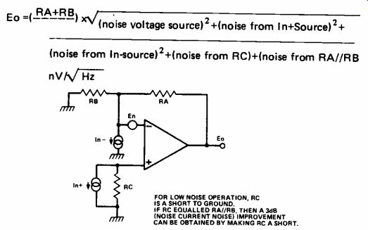
Fig.11. Model of op amp noise generation.
The noise performance curves for a low noise op amp, the SE5534, are shown in Fig.12a,b,c. Graph a shows the input noise voltage density, En (ie total RMS noise in a 1 Hz band width at that particular frequency), as a function of frequency. To convert this input noise voltage, (4nV/N/FiT ) into an equivalent input noise generator, we must define the bandwidth of interest. As the noise spectrum is relatively flat above 100 Hz then we can say,
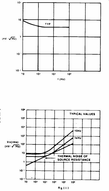
Fig.12a.The SE5534 low noise op amp input noise
voltage density.
Fig.12b. The variation in total input noise density with source resistance for two frequencies.
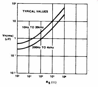
Fig.12c. The equivalent input noise voltage for two bandwidths
as a function of frequency.
The equivalent input noise voltage
Ein (En2xbandwidth2) For 20 kHz bandwidth Ein = (En2 x20,0002) Ein = (En x 141) nV RMS But En = 4nVN/f7IT
Therefore Ein = 4x141 = 0.564 uVRMS (20 kHz)
Design Example
Q. Calculate the output noise in a 20 kHz bandwidth for the circuit in Fig.13. Assume the voltage and current densities have a flat spectrum (which is not too far from the truth!).
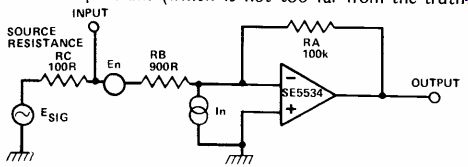
Fig.13. A low noise amplifier.
A. Calculate the individual noise sources.
Resistor Noise Effective resistor is RA//(RB+RC) 1 kO
Therefore thermal noise (from Fig.13b)= 3 nVW-H-z Noise Voltage a = 4 nV/N./H7
Noise Current
c = 0.5pA/V-Hz which sets up a noise voltage through (RB + RC).
This noise voltage is 0.5pA x 1 kO = 0.5 nV/VHZ
Therefore the total noise voltage Eo = ( RA+RB+RC ) x J (4)2 + (0.5)2 + (3)2 RA+RB
= 101 x/16+0.25+9
= 101 x\/25.25 500 nV/VHz
For 20 kHz bandwidth, the output noise = 500 x 141
= 70,500 nVRMS
= 70.5 uVRms
A 7 mVRMS input signal from, say, a low impedance micro phone would result in a 700 mVRMS output signal and give a S/N ratio of 20 Logo s ) 80 dB Note that most dominant source in this circuit is the noise generator En. As long as the input impedance levels are kept low, then it is the noise generator En on its own that can be used as a rule of thumb for calculating absolute and comparative noise performance. For high input impedance applications a FET op amp (with virtually no input noise current) should be used.
Noise Measurements
The noise current voltage spectrums of Fig.12 were measured using a mobile analyzing filter (1 Hz bandwidth) plus an RMS meter. A simpler measurement can be performed using the system shown in Fig.14. This will measure the equivalent input noise in a specified bandwidth. The low pass filter should be high order device with a steep roll off slope. If a single pole low pass filter is used, then the RMS reading should be corrected by the following equation,
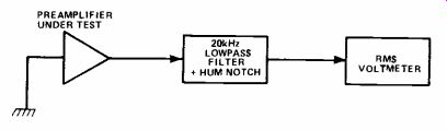
Fig.14. Noise measurement.
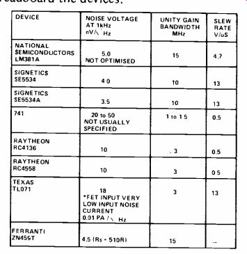
Fig.15. Opamp performance.
'True' RMS noise (for a one pole lowpass filter) measured RMS noise 1.57 (An RC 20 kHz low pass filter would be made from an 820 ohms resistor with a 10 n capacitor to ground).
Sometimes the signal to noise ratio is quoted in dBA.
This means that the noise measurement has been modified by an A weighted curved.
A short chart of op amp performance has been drawn up in Fig.17. It is difficult to compare device performance merely from the noise voltage at one frequency in the spectrum, as the noise spectrum shapes are different from device to device.
It is best to refer to the manufacturing data sheet and then to actually breadboard the devices.
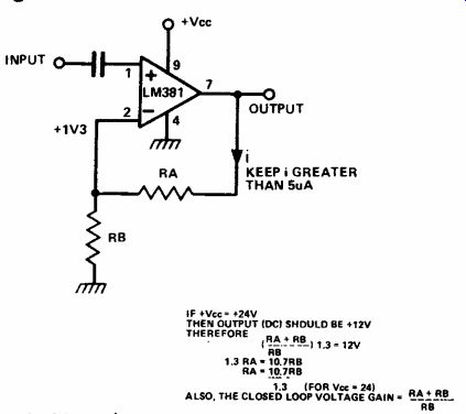
Fig.16. Biasing the LM381 (differential mode).
The base of Q1 is held at +1V3 by a pair of diodes. This preamplifier is often run from a single supply rail and a simple resistor network can be used to bias the output voltage to 1/2 Vcc (Fig.16). Also a single ended amplifier can be constructed (Fig.17). The resistor pair RA, RB determines the DC output level and gain. To increase the AC gain resistor RB can be shorted to ground with a series R,C network.
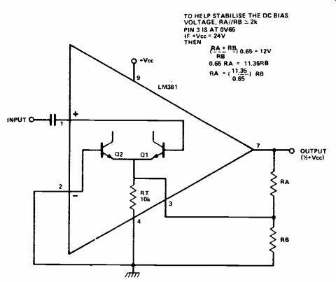
Fig.17. Single -ended biasing.
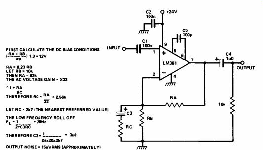
Fig.18. A 30 dB amplifier.
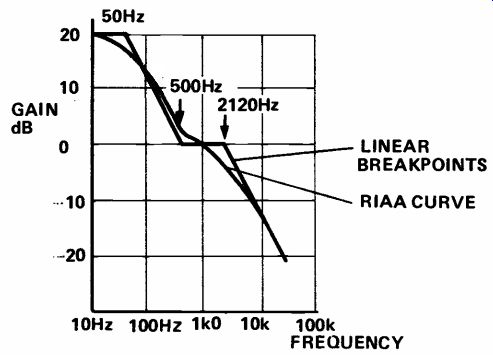
Fig.19. RIAA equalization.
Design Example
Q. Design a preamplifier using the LM381 with a gain of 30 dB and a low frequency roll off of 20 Hz running from a +24 V power supply.
A. The design calculations are shown in Fig.18.
Record Preamplifier
When replaying a record from a magnetic cartridge it is necessary to have a preamplifier with an RIAA playback equalization (Fig.19). A magnetic pick up generates a voltage that is proportional to the velocity of the sideways movement of the stylus. So high frequencies produce large outputs and vice versa. Also, to assist replay electronics, the recording is given a 12 dB de-emphasis from 500 Hz to 2120 Hz. Thus, to restore a flat output it is necessary to equalize the signal from the pick up with an RIAA curve. As a rule of thumb, a typical magnetic pick up will generate 5 mVRMS at 1 kHz, although the recording level and make of pick up will effect this figure.
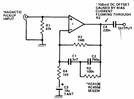
Fig. 20. An RIAA-equalized preamplifier.
Low-frequency gain = R4 = 60 dB Low frequency rolloff =
1 50 Hz breakpoint 2irR4C3 2/r R2C1 - 15 Hz
The gain drops at --6 dp/octave beyond this point 500 Hz breakpoint 27rR3C1 Now the gain remains constant until the next breakpoint AC gain at 1 kHz = R3 = 40 dB R4 1 2120 Hz breakpoint 2irR3C2
The gain now falls at -6 dB/octave beyond this frequency.
A 5 mVRMS signal at 1 kHz will result in a 500 mVRMS (1V4 pp) at the preamplifier output. If the amplifier is powered from ±12 V, then there is an overhead margin of ( maximum output swing = 20 V) = 14, typical swing = 1V4 which is 23 dB. The noise spectrum of the op amp will be multiplied by the RIAA curve which would complicate any noise performance calculations. However, an op amp with an equivalent input noise of 0.5 uV should give a signal to noise performance of better than 76 dB which is superior than that of the disc itself. Because of the large low frequency gain care must be taken to avoid mains hum pick up. Keep the input wiring away from the mains cables and transformers, use low noise screened cable and wire this cable as close as possible to the preamplifiers.
Problems
Often a preamplifier will pick up radio signals. Usually, the radio signal is picked up by the input wiring to the pre amplifier and is rectified by the transistor input stage. Then it is amplified by the rest of the audio amplifier and you end up with permanent broad band radio reception. There are several solutions that can be tried, Fig.21. A low pass filter made from an LC or an RC section will attenuate the 'pick up' interference. These devices must be physically close to the op amp. If possible use a PCB ground plane. Also, a conductive metal screen (metal foil is often used) surrounding the preamplifier will help.
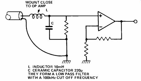
Fig. 21. Removing RF interference.
Hum can also be a problem. If the hum is at 50 Hz then the source of it is probably magnetic. Check the wiring to see if any signals pass near to the mains section. Magnetic screening is difficult to implement. The best design solution is to put as much distance between the sensitive input and the mains section as possible. If it is possible try rotating the mains transformer (using a gloved hand, the other hand in your pocket). Often the size of the hum can be reduced by re-orientating the transformer. If the hum is 100 Hz, then the source is either the supply rails or the power supply layout. A larger smoothing capacitor will reduce the power supply ripple. If the hum has a sharp buzz then the problem is probably the charging current pulses in the power supply. If the layout is bad, these current pulses generate voltage pulses that get added into the ground reference voltage, thus causing the hum.
Gain When designing an audio system it is necessary to know what the normal signal level at any point will be and also the signal gains and attenuations of various units. It has been found that the most useful way to describe levels and gains is with the logarithm decibel, Fig.22. Signal gains in dB are additive. That is, a signal passing through a series of gains of +10, +20, -30, +6 dB will end up with an overall gain of +6 dB.
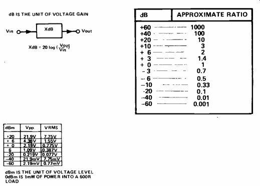
Fig. 22. The dB and dBm story.
A typical audio system is shown in Fig.23. A low impedance microphone might typically give a -50 dBm output signal which will have to be given a 56 dB (x 600) gain to bring it up to line level (about +6 dBm). The line driver should be capable of driving +20 dBm into 600 ohms at 20 kHz without generating significant distortion. Some line drivers are, in fact, capable of driving 30 ohm loads, but these units are small high quality power amplifiers.
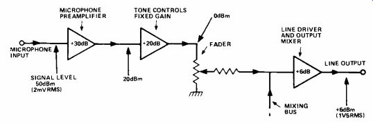
Fig. 23. One channel of a mixing desk.
+++++++++++++++++++
2. LARGE SIGNAL, OR POWER, AMPLIFIERS
A power amplifier must deliver power into a load without generating significant distortion or bursting into oscillation or burning itself out. Power amplifiers are, however, prone to all these effects and great care is needed during their design.
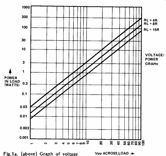
Fig.1a. (above) Graph of voltage against power.
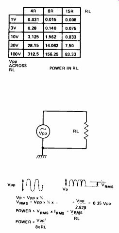
Fig.1b. (left) The power dissipated in a load against drive
voltage.
Fig.1c. (left) The measurement of power.
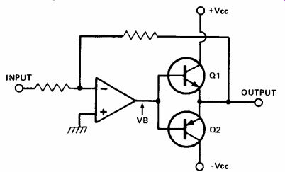
Fig. 2. A simple power amplifier.
Power
Power is measured in watts and is defined as the product of VRMS x IRMS (Fig.1c), where RMS is the equivalent DC value. That is, a 2 Vpp sinewave has the DC value of 0V7. The 2 Vpp sinewave will generate as much heat in a load as a 0V7 DC voltage. The chart in figure lb shows the power dissipated in a load against drive voltage. If you have an amplifier that has a maximum output voltage swing of ±10 V, then the maximum power output will be 12.5 watts into a 4 ohm load (from Fig.1 a). Note that the amplifier must be able to deliver a peak current of 2.5 Amps. Whilst dumping power into the load, the amplifier will be dissipating heat itself. Most monolithic devices are documented with design graphs of output power versus amplifier dissipation of power efficiency. These will enable you to determine the amplifier's maximum power dissipation. As a rule of thumb, this equals the maximum sinewave power that can be dumped into the load. A 10 watt amplifier may have to dissipate a maximum of 10 watts of heat, although this level of dissipation would not be normal in general use. Manufacturers information usually gives the thermal resistance of the junction to case. If this was say 3°C/watt then a 10 watt dissipation would raise the junction temperature by 30° above ambient (25° raising to 55°C).
This is only true if the case temperature remains at ambient temperature, that is if the case is contact with an infinite heat sink. The heatsink may be anything from nothing (free air dissipation) to near infinite. It is important that the amplifier chip junction does not get very hot (above 100°C). The power chips of the amplifier age very quickly at elevated temperatures suffering from deteriorating characteristics and a short life time. This is why power amplifiers and power supplies are common failures in equipment. When the chip is heated up it expands. The chip is glued to its case and so by expanding it stresses the glue and eventually causes it to fracture. This thermal cycling increases the thermal resistance of the chip to the case and so the chip ends up operating at an even higher temperature.
Other heatsinking materials are used in the construction of power devices such as heat conducting plastics and pastes (Beryllium oxide). Manufacturers often provide design graphs of maximum dissipation versus temperature for various heatsink thermal resistances. These help to select an acceptable heatsink. Often if you are using the chassis as a heatsink it is impossible to calculate the temperature rise and it has to be done by trial and error. (As a rule of thumb I am satisfied if I can place my finger on the device for 5 seconds indicating that case temperature is no more than 80°C).
Distortion
A simple power amplifier is shown in figure 2. An op amp provides the voltage gain and a NPN, PNP transistor pair forms a current amplifier. Any distortions or nonlinearities are ironed out by the surplus loop gain of the op amp. The transfer characteristic of Q1, Q2 shows that there is a dead zone of ±0V6 where neither transistor is ON. If a low frequency sinewave is connected to the input (the op amp having a surplus loop gain of 1000 at this frequency) then the output will be a sinewave with a small amount of crossover distortion. The distortion level will be ± 0V6 = ± 0.6 mV.
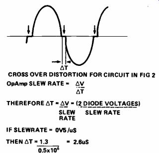
Fig. 3. The effect of slew rate at higher frequencies.
However, as the frequency is increased, the surplus loop gain will decrease causing the distortion to rise. At higher frequencies the slew rate of the op amp becomes noticeable (Fig.3). When the input signal crosses 0 V the output of the op amp has to change from +0V6 to -0V6. If the slew rate is 0V5/uS then the time taken to travel the 1V2 distance is 2.6 uS. Thus a 2.6 uS chunk of the signal is missing out of each half cycle. The problem may be overcome by biasing the two transistors so that they are both conducting. Then the crossover distortion becomes reduced to a reasonable level.
The slew rate still needs to be considered. An amplifier delivering a 40 Vpp sinewave at 20 kHz has a fastest slew rate of 2V5/uS (this represents a power of 25 watts into 8 ohms).
If the amplifier has not enough slew rate the output will become distorted. Manufacturers generally provide graphs of distortion (THD) versus power output and frequency (Fig. 4). For the power curve, the onset of distortion is caused by the amplifier clipping at its power rails, whereas for the frequency curve the distortion rises as the surplus loop gain falls.
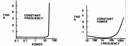
Fig. 4. THD versus power and frequency.
Distortion is measured at various power levels and frequencies using the equipment shown in figure 5. A deep notch removes the test sinewave leaving behind the distortion products.
Generally 0.1% THD is common for monolithic amplifiers.
Stability Power amplifier performance is very similar to that of op amps. They have a large open loop gain that is stabilized by resistive feedback (Fig.6). Note that the amplifier described in this graph is normally inverting (180° DC phase shift) but that it suffers a phase shift as the frequency increases. The phase shift at the unity gain frequency is shown as the phase margin. If the phase margin falls to zero anywhere before the unity gain frequency then the amplifier will oscillate. This is simply because the loop phase shift will be zero at a loop gain of greater than unity, which are the conditions for an oscillation. A large phase margin is desirable.
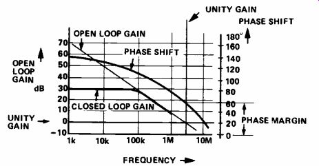
Fig. 6. Gain and phase response.
Various techniques are available for preventing instability.
Often a series RC network is connected from the amplifiers output to ground. This reduces the high frequency gain and thus reduces the unity gain frequency. Local power supply decoupling should be used. Current loops, whereby the output current generates a voltage in the signal ground wire which gets fed back to the input can cause bursts of high frequency oscillation. Also high input impedances can capacitively pick up the output signal and burst into oscillation. Increasing the closed loop gain may prevent some forms of instability, swearing will not! Figure 7 shows some typical instability problems.
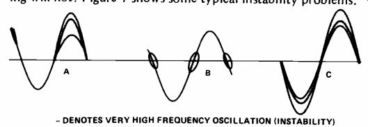
Fig. 7. Instability; A, on one half cycle; B, at crossover;
C, at all points.
(a) The sinewave oscillates on one half cycle. Really a power amplifier is two amplifiers, one half handling positive signals, the other, negative signals. Thus it is quite possible that the amplifier can be stable for negative signals but not positive ones.
(b) The sinewave is unstable at crossover. This may be caused by the loss of feedback at crossover. Increasing the bias current may eliminate it. Alternatively it might be caused by slew limiting manifesting itself as an extra phase shift.
(c) The amplifier is never stable. Check the layout for current loops, increase the gain, increase the output CR loading, even try removing it, reduce the impedance levels.
You may not hear the effects of high frequency oscillation but it does cause RF interference and generates waste power. It can burn out output stages and even loudspeaker crossovers.
The following five design examples demonstrate how to produce a solution to an amplifier problem. It is now possible to buy an amplifier for most general purpose uses. A wide selection of monolithic devices and modules cover the 0.25 to 100 watt power range. It is rare to have the time or the ability to improve upon this range. The art of designing is to select the most suitable solution on the basis of size, cost and performance.
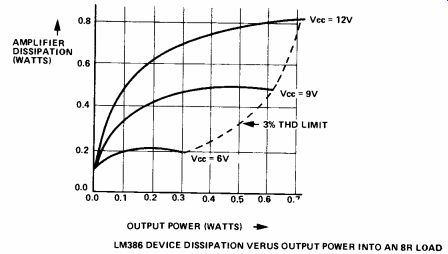
Fig. 8. Low voltage, low power battery operated amplifier.
The LM386N operates over a supply range of 4 to 12 V. It can
deliver 0.7 watts into 8 ohms at 12 V, although, at this level,
some heatsinking would be advisable. The typical battery drain
is 4 mA. The voltage can be varied from 20 to 200, as shown
it is 20. An AC short across pins 1 and 8 will increase the
gain to 200. With a resistor in series the gain can be set
to anything from 20 to 200. For gains greater than 20, a bypass
capacitor (100n to ground from pin 7) should be used. Even
with a supply voltage of only 4 V, there is an output voltage
swing of greater than 2 V.
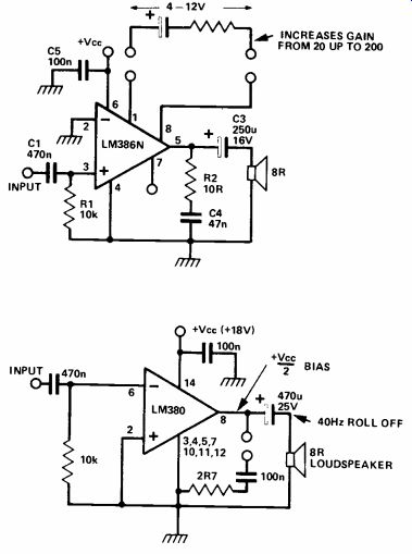
Fig. 9. Medium power audio amplifier. The LM380 will work
with a supply voltage range of 8 to 22 V. It can deliver 4
watts of power into 8 ohms at 20 V, although a good heatsink
is needed for this level. The inputs are ground referenced
and the output is automatically biased to 1/2 Vcc. The voltage
gain is fixed at 34 dB. It also has a short circuit proof output
and internal thermal limiting.
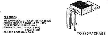
Fig.10. 9 to 14 watt amplifier. The TDA2030 is a Hi-Fi audio
amplifier which has short circuit protection and thermal shutdown.
It can operate from supply rails of ± 6 to ± 18 V. At a ± 14
V supply the guaranteed output power is 12 watts into 4 ohms
and 8 watts into 8 ohms.
Harmonic and crossover distortion is low being typically 0.05% at 1 kHz for 7 watts of power output. The recommended closed loop gain is 30 dB. The two diodes protect the amplifier from back EMF voltages from the speaker.
+++++++++++++++++++
3. OSCILLATORS
It seems to be a fact of life that amplifiers oscillate and oscillators won't! Generally there is little difference between the two. Both devices are amplifiers with feedback.
The conditions for stable sinusoidal oscillation are shown in Fig.1. The higher the Q of the resonator the more stable is the resonant frequency, and the purer the sine wave. To stabilize the signal level an automatic gain control circuit is used. This can be anything from simple diodes or thermistors to elaborate AGC systems. The smoothness with which the AGC works will determine the sine wave purity. A thermistor circuit might well introduce distortion at low frequencies by changing its resistance during one half cycle of oscillation. Very pure sinewave oscillators (better than 0.001% distortion) employ slow acting AGC systems to control the loop gain.
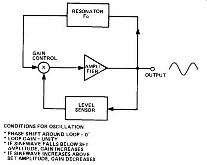
Fig.1. Conditions for a stable sine wave oscillator.
Wien Bridge
The well known Wien Bridge oscillator is shown in Fig.2a.
A frequency sensitive feedback network is constructed from R1, C1 and R2, C2. This network has a peak in its amplitude response which also corresponds to zero phase shift. At this frequency the attenuation is x1/3 and so to ensure oscillation the amplifier must have a voltage gain of at least x3.
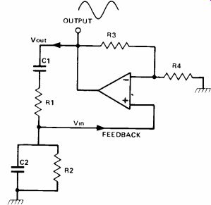
Fig.2a. A Wien Bridge oscillator.
Fig. 2b. To stabilize the amplifier a thermistor is used in
the op amp feedback loop.
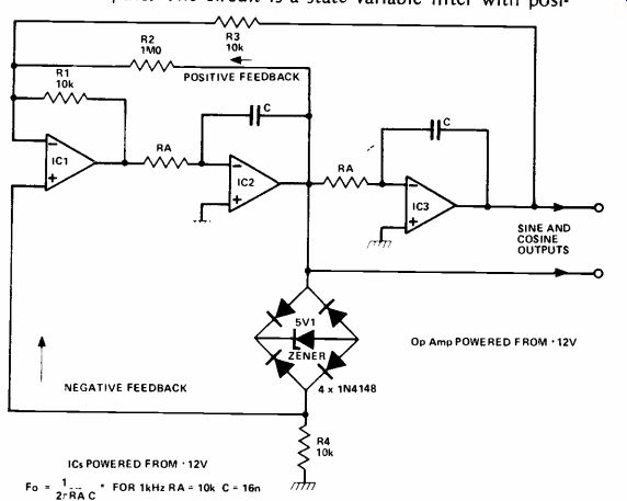
Fig. 3. A state variable sine/cosine oscillator.
To stabilize the amplitude a thermistor is used in the feedback loop of the op amp. As the oscillation amplitude increases, the thermistor heats up, drops in resistance and so reduces the gain. The circuit suffers from amplitude bounce when the frequency is altered. Also, the op amp phase shift, which increases with increasing frequency, must be taken into consideration when designing this oscillator. Another sine wave oscillator is shown in Fig.3. This generates both sine and cosine outputs. The circuit is a state variable filter with positive feedback (R2) to ensure oscillation and amplitude limiting (the diode bridge) to stabilize the sine wave level. The distortion may be trimmed by adjusting the amount of positive feedback. The oscillation frequency is set by RA and C.
A triangle/square wave oscillator may be constructed from a pair of op amps (Fig.4). IC1 is an integrator, the output of which ramps up and down between the hysteresis levels set by the Schmitt trigger, IC2. If the output of IC2 can swing to ± 10 V then the hysteresis level will be ± 10 x RA - volts RB
The oscillation frequency and triangle symmetry is linearly proportional to the output swing of IC2. If a variable frequency oscillator is wanted, then resistor R can be connected to the wiper of a potentiometer fed from IC2 output.
Design Example
Q. Design a triangle oscillator with a 2 Vpp triangle output, oscillation frequency of 1 kHz, operating from ± 12 V power supplies, using circuit in Fig.4.
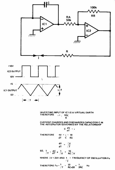
Fig.4. A triangle/square wave oscillator.
A. Assume an output voltage swing at IC2 of ± 10 V.
For ± 1 V Hysteresis, RA = RB 10 Let RB = 100k, then RA = 10k Fo = 1 kHz =
1 10 AT iAv Cx Rx 4
Therefore CR =
10 4x1000
= 2.5 x 10⁻³ Let C = 100n
Then R 2.5 x 1°-3 = 25k 10^-7
AV
Note that Af is 4000 V/sec.
When designing this type of oscillator the slew rate of the integrator and Schmitt trigger need to be considered, although tin this case virtually any op amp will be OK.
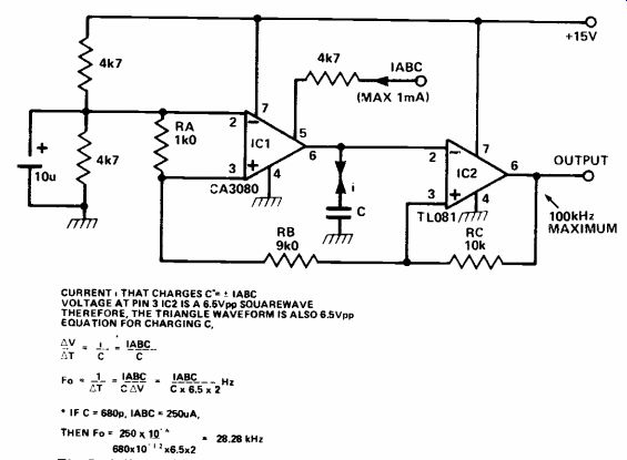
Fig.5. A linear VCO.
Linear VCO
A linear voltage controlled oscillator (VCO) is shown in Fig.5. This again is a triangle square wave oscillator although the squarewave is the only buffered output. The CA3080 is used as a current source for charging and discharging C. The charging current is equal to !ABC, which is true for several decades of current. The Schmitt trigger uses a TL081 which has a slew rate of 13 V/uS. As the squarewave output voltage is 13 V then the rise and fall times are 1 uS each. This enables the VCO to run at frequencies up to 100 kHz. As this frequency is approached the VCO loses its linearity, due to time delays in the circuits.
Another VCO is shown in Fig.6. This has two buffered outputs, a triangle and a square wave. Again, the oscillation frequency is dependent on the output voltage swing of the Schmitt trigger, IC2. However, if a stabilized power supply is used this circuit behaves very well. Superior performance can be obtained by replacing Q1 with a switching FET. The aberrations caused by saturation voltage and storage time are then removed. Also fast FET op amps will improve high frequency performance.
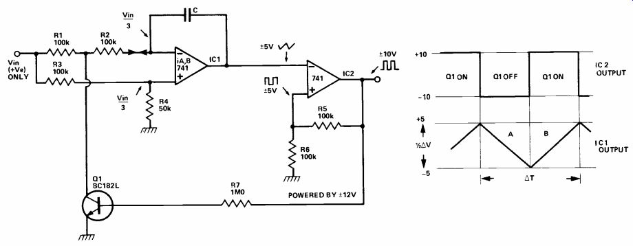
Fig. 6. A linear triangle/square wave VCO.
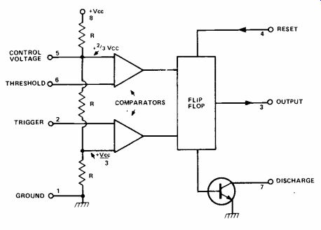
Fig.7. The timer chip.
The 555
The 555 timer chip (Fig.7) can be used as an oscillator (Fig.8). Capacitor C is charged up via RA and RB. When the voltage at pin 6,2 reaches 2/3 Vcc the discharge transistor is turned ON. When the voltage falls to 1/3 Vcc the discharge Vcc
transistor is turned OFF and the charging process repeats itself. As power supply voltage terms appear in both the numerator and denominator of the charging equation, it drops out and so the oscillation frequency is hardly effected by supply voltage changes (typically 0.3%V). Also the temperature stability is good, typically 50 ppm/°C.
A low power 555 oscillator is shown in Fig.9. This employs a CMOS version of the chip which consumes a mere 120 uA. Capacitor C is slowly charged by current i and rapidly discharged by Q1.
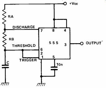
Fig. 8. A simple oscillator based on the 555.
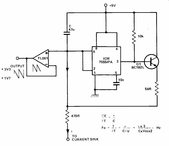
Fig. 9. A linear VCO built around the ICM7555, the CMOS 555.
(adapted from: Electronics Digest (Vol. 2 No. 3--WINTER 1981))
NEXT: