AMAZON multi-meters discounts AMAZON oscilloscope discounts
PART 1
GOALS:
1. Demonstrate an understanding of reactance, resonance, transformers and transfer and the practical application of these components and circuits
2. Demonstrate an understanding of semi-conductor devices, displays and transducers and the practical applications of these components.
Sine wave driven circuits
Capacitors and inductors in direct current ( d.c.) circuits cause transient current effects only when the applied voltage changes. In an alternating current (a.c.) circuit this is a continuous process. Capacitors in such a circuit are therefore continually charging and discharging, and inductors are continually generating a changing back-electromotive force (emf). Circuits containing resistors, capacitors and inductors are described as complex circuits and an alternating voltage will exist across each component proportional to the magnitude of current flowing through it so that a form of Ohm's law still applies.
In the explanation that follows, the symbols V' and I' are used to mean peak a.c. values (FIG. 1) of alternating signals. Root mean square (r.m.s.) values are represented by Vrms and Irms; that is, I' rms = I' __/2 . The symbols v and i represent instantaneous values of a.c. signals and V and I will have their usual meaning of d.c. values. So, we may write v = V’ sin (2 pi ft).
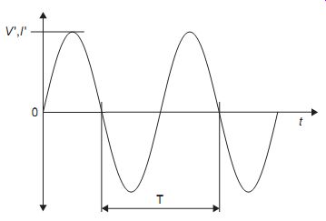
FIG. 1 The peak value and period of a sine wave of voltage or current
_ _
For a resistor in an a.c. circuit, V_ _ R _ I_ and the value of resistance found from the variant form of this equation, R= V'/ I' , is the same as the d.c. value, V/I. In a capacitor or an inductor, the ratio V'/I' is called reactance, with the symbol X. Because this is a ratio of volts to amperes, the same units Ω (O, ohms) are used as used to express d.c. resistance, but it must be remembered this is a frequency-dependent reactance and not a resistance.
A capacitor may, for example, have a reactance of only 1 KO at a given frequency, but a d.c. resistance that is un-measurably high. An inductor may have a d.c. resistance of 10 ohms, but a reactance of 5 KO or more. The reactance of a capacitor or an inductor is not a constant quantity, but depends on the frequency of the applied signal. A capacitor, for example, has a very high reactance to low-frequency signals and a very low reactance to high frequency signals, as indicated in FIG. 2.
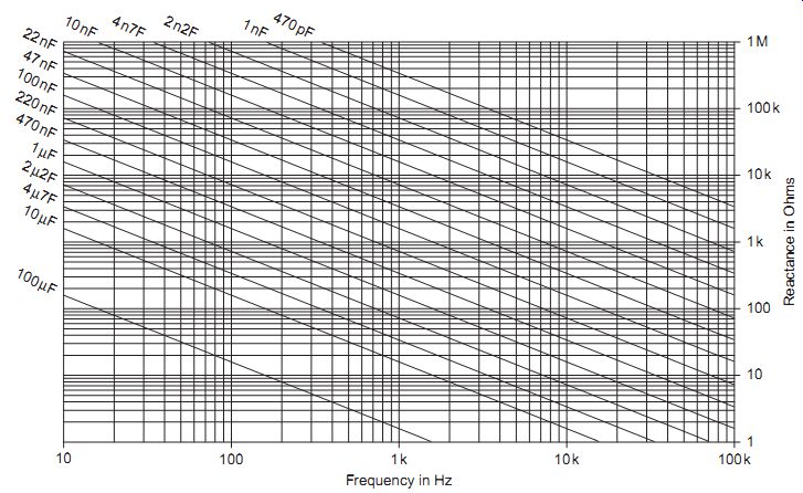
FIG. 2 Chart of capacitive reactance at audio frequencies
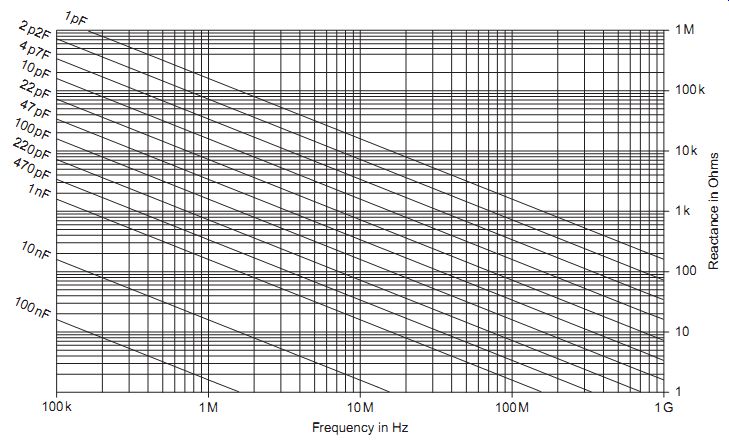
FIG. 3 Chart of capacitive reactance at radio frequencies
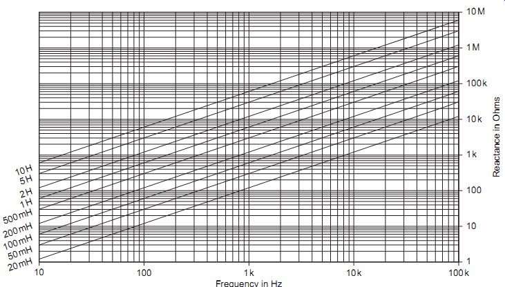
FIG. 4 Inductive reactance at audio frequencies
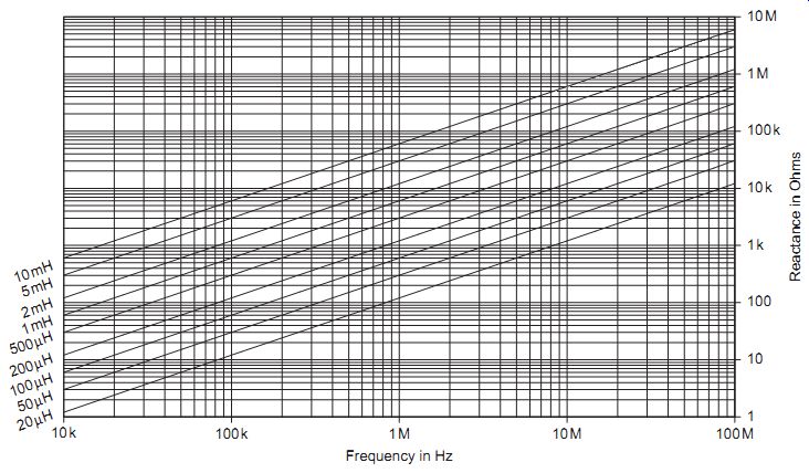
FIG. 5 Inductive reactance at radio frequencies
The reactance of a capacitor V'/I' can be calculated from the equation:
Xc= 1 /2 pi fC ohms
where f is the frequency of the signal in Hz and C is the capacitance in farads. Figures 2 and 3 show the values of capacitive reactance for a range of different capacitors calculated for a range of frequencies. These charts are intended as a guide so that you can quickly estimate a reactance value without the need to make the calculations.
The reactance of an inductor varies in the opposite way, being low for low-frequency signals and high for high-frequency signals. Its value can be calculated from the equation:
XL _ 2 pi fL ohms
where f is the frequency in Hz and L is the inductance in henries. Figures 26.4 and 26.5 show the values of inductive reactance which are found at various frequencies.
Note: inductors are now less common in circuits other than power sup ply and radio (transmission and reception) applications. The increasing use of integrated circuits (ICs) and digital circuitry has made the use of inductors unnecessary in a very wide range of modern applications.
---------------------
EXPERIMENT 1
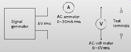
FIG. 6 Circuit for practical
Connect the circuit shown in FIG. 6. If meters of different ranges have to be used, changes in the values of capacitor and inductor will also be necessary. The signal generator must be capable of supplying enough current to deflect the current meter which is being used.
Connect a 4.7 µF capacitor between the terminals, and set the signal generator to a frequency of 100 Hz. Adjust the output so that readings of a.c. voltage and current can be made. Find the value of V_/I_' at 100 Hz.
Repeat the measurements at 500 Hz and at 1000 Hz.
Tabulate values of XC _ V_/I_ and of frequency f.
Now remove the capacitor and substitute a 0.5 H inductor. Find the reactance at 100 Hz and 1000 Hz as before, and tabulate values of XL _ V_/I_ and of frequency f.
Next, either remove the core from the inductor or increase the size of the gap in the core (if this is possible), and repeat the measurements. How has the reactance value been affected by the change?
--------------------------
There is another important difference between a resistance and a capacitive or inductive reactance and this can be demonstrated as follows. With the aid of a double-beam oscilloscope, the a.c. waveform of the current flowing through a resistor and the voltage developed across it can be displayed together (FIG. 7). This shows that the two waves coincide, with the peak current coinciding with the peak voltage, etc. If this experiment is repeated with a capacitor or an inductor in place of the resistor, you will see from the figure that the waves of current and voltage do not coincide, but are a quarter-cycle (90º) out of step.
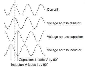
FIG. 7 Phase shift caused by a reactance
Comparing the positions of the peaks of voltage and of current, you can see that:
• For a capacitor, the current wave leads (or precedes) the voltage wave by a quarter-cycle.
• For an inductor, the voltage wave leads the current wave also by a quarter-cycle.
An alternative way of expressing this is that, for a capacitor, the voltage wave lags (or arrives after) the current wave by a quarter-cycle, and for an inductor, the current wave lags the voltage wave by a quarter-cycle.
The amount by which the waves are out of step is usually defined by the phase angle. The current and voltage waves are 90º out of phase in a reactive component such as a capacitor or an inductor.
A useful way to remember the phase relationship between the current and voltage is the word C-I-V-I-L, meaning C-I leads V; V leads I-L. The letters C and L are used to denote capacitance and inductance, respectively.
If we take a few measurements on circuits containing reactive components we can see that the normal circuit laws used for d.c. circuits cannot be applied directly to a.c. circuits.
Consider, for example, a series circuit containing a 10 µF capacitor C, a 2 H inductor L and a 470 ohm resistor R, as in FIG. 8(a). With 10 V a.c. voltage, V_ at 50 Hz applied to the circuit, the a.c. voltages across each component can be measured and added together: V' C+ V' L+ V' R. You will find that these measured voltages do not add up to the voltage V' across the whole circuit.
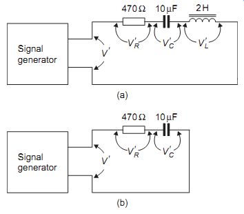
FIG. 8 Series circuits: (a) RLC, and (b) RC circuit for practical
example
---------------------
EXPERIMENT 2
Connect the circuit shown in FIG. 8(b). Use either a high resistance a.c. voltmeter or an oscilloscope to measure the voltage V_ R across the resistor and the voltage V_ C across the capacitor. Now measure the total voltage V' and compare it with V' R + V' C.
-----------------------
The reason why the component voltages in a complex circuit do not add up to the circuit voltage when a.c. flows through it is due to the phase angle between voltage and current in the reactive component(s). At the peak of the current wave, for example, the voltage wave across the resistor will also be at its peak, but the voltage wave across any reactive component will be at its zero value. Measurements of voltage cannot, however, indicate phase angle. They can only give the r.m.s. or peak values for each component, and the fact that these values do not occur at the same time cannot be allowed for by meter measurement. The result is that straight addition of the measured value will inevitably give a wrong result for total voltage, because of the time difference.
Phasor diagrams (often also called vector diagrams) are one method of performing the addition so that phase angle is allowed for. In a phasor diagram, the voltage across a resistor in an a.c. series circuit is represented by the length of a horizontal line drawn to scale. Voltages across reactive components are represented by the lengths of vertical lines, also drawn to the same scale. If all the lines are drawn from a single point, as in FIG. 9(a), the resulting diagram is a phasor diagram that represents both the phase and the magnitude of the voltage wave across each component.
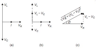
FIG. 9 Phasor diagrams for complex series circuits: (a) relationship
between V and I for a series RLC circuit, (b) combining VL and VC, and
(c) finding the total voltage across the circuit.
To represent the opposite effects that capacitors and inductors have on the phase, the vertical line representing voltage across an inductor is drawn vertically upwards, and the line representing voltage on a capacitor is drawn vertically downwards. By convention, an inductive reactance and the voltage across it are considered to be positive. A capacitive reactance and its voltage are considered to be negative.
The phasor diagram can now be used to find the total voltage across the whole circuit. First, the difference between total upward (inductive) and total downward (capacitive) voltage is found, and a line is drawn to represent the size and direction of this difference. For example, if the inductive voltage is 10 V and the capacitive voltage 7 V, the difference is 3 V drawn to scale in the direction of inductive reactance. If the inductive voltage were 10 V and the capacitive voltage 12 V, the difference would be 2 V drawn to scale downwards in the capacitive direction.
The net reactive voltage so drawn is then combined with the voltage across the resistor in the following way. Starting from the point marking the end of the line representing the voltage across the resistor, draw a vertical line, as in FIG. 9(b), to represent the net reactive voltage in the correct direction, up or down. Then connect the end of this vertical line to the starting point (FIG. 9c). The length of this sloping line will give the voltage across the whole circuit, and its angle to the horizontal will give the phase angle between voltage and current in the whole circuit.
The total voltage can be found by Pythagoras' rule, since the phasor relationship is that of a right-angle triangle, so the total voltage is
V'T= √(VVVV TRLC _ _ 222).
A complex circuit which contains both resistance and reactance possesses another characteristic which is of great importance. This characteristic is known as impedance, symbol Z. Impedance is measured in ohms, and is equal to V'/I' for the whole circuit. Its value varies as the frequency of the signal varies.
When impedance is present, the phase angle between current and voltage is less than 90º in either direction. This phase angle can be found most easily by using the phasor diagram in a slightly different way, to form what is known as the impedance triangle.
In a phasor diagram constructed this way (FIG. 10), separate lines are drawn to represent the resistance R, the reactance X and the impedance Z. In a series circuit, the length of the horizontal line represents the total value of resistance in the circuit, and the vertical line its net value of reactance upwards as before, for predominantly inductive reactance (a), and downwards for predominantly capacitive reactance (b).
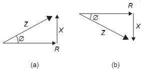
FIG. 10 Impedance triangle: (a) predominantly inductive, and (b) predominantly
capacitive
With the values of R and X known and the angle between them a right angle, the Z line can be drawn in, representing the impedance value of the whole circuit. The angle of this line to the horizontal is the phase angle between current and voltage in the circuit.
Another way of working out the relationships between R, X and Z in a complex circuit is to express them by two algebraic formulae:
ZXX R XXR LC LC ___ __ () )/ 22 and tan ( ?
where Z _ total impedance, XL _ inductive reactance, XC _ capacitive reactance, ? _ phase angle, and R _ the resistance of the circuit as a whole.
A pocket calculator covering a reasonably full range of mathematical functions can now be used to work out the values of circuit impedance and phase angle.
Filters
Filters are circuits that are designed to separate out a range of frequencies of interest that are present in any waveband. Because these are frequency dependent, the circuits must contain at least one reactive component.
In the low-pass filter (LPF) shown in FIG. 11(a), the inductor has a low series reactance at low frequencies so that these pass easily to the output and are developed as the output signal Vout. In FIG. 11(b), the capacitor has a very high reactance at low frequencies and acts as the load to develop the output signal Vout. At high frequencies the low reactance of C effectively short-circuits the output signal.
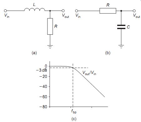
FIG. 11 Low-pass filters: (a) LR, (b) CR, and (c) typical response
FIG. 11(c) shows the amplitude of the output signal plotted against
frequency for both the LR and CR circuits and this also represents the
variation of circuit impedance with frequency. The _3 dB or half power
point of the frequency response represents the break point where the circuit
reactance is equal to its resistance value. This point is defined by the
formula f _ 1/(2pCR) Hz or f _ 1/(2p(L /R)) Hz and is therefore dependent
on the circuit time constant.
For the high-pass filters (HPFs) shown in FIG. 12(a, b), the resistors and reactors are interchanged to produce the opposite effect. FIG. 12(c) again shows the attenuation effects and the variation of circuit impedance, with the break point calculated as before.
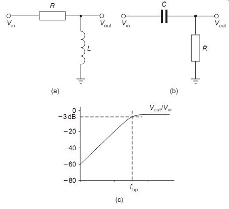
FIG. 12 High-pass filters: (a) LR, (b) CR, and (c) typical response
For both of the first order LPF and HPF circuits with a single pair of components shown above, the straight part of the attenuation slope falls away at 6 dB per octave (a doubling or halving of frequency).
----------------
EXPERIMENT 3
For an LPF and an HPF as shown in Figures 11 and 12, set up a circuit so that the signal current through the filter can be plotted against frequency. How do these results compare with the shape of the attenuation characteristics?
------------------
A circuit that selects a band of frequencies is described as a band-pass filter (BPF) and one such circuit can be constructed as shown in FIG. 13.
This is effectively a cascade of an LPF and an HPF and its attenuation characteristic is shown in FIG. 13(b). The attenuation slope at both ends is still _6 dB per octave. The two _3 dB break points of the individual low- and high-pass sections are calculated from the equations
f1f _ 1/(2pC1R1) Hz and fhf _ 1/(2pC2R2) Hz
and if the stages did not load each other the bandwidth of the circuit would simply be the difference between these two frequencies. This is rarely the case for practical values and in effect the high- and low-pass corners are pulled towards each other by the loading effects. This type of filter can suffer from quite large in-band insertion losses, particularly if the RC sections are chosen to minimize load effects; it is often useful to put a buffer amplifier in between the stages to restore the losses and isolate the stages from each other.
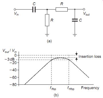
FIG. 13 (a) Band-pass filter circuit, and (b) typical response A
band-stop filter (BSF), which has the opposite characteristic of the BPF,
cannot be conveniently constructed using the cascading principle shown
above.
For these circuits it is more usual to use second order filters as shown in FIG. 14(a). This particular circuit is referred to as a twin or parallel T device, where the ratios of the component values are chosen as:
C2 _ 2C1 and R1 _ R2/2 so that the maximum attenuation occurs at f _ 1/(2pR1C1) Hz.
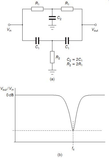
FIG. 14 Band-stop filter (twin-T): (a) circuit, and (b) typical response
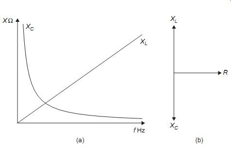
FIG. 15 Resonance in a series LCR circuit
Resonance
The values of capacitive reactance, XC, and inductive reactance, XL, are frequency dependent but have opposite slopes. At low frequencies, XC is large and XL small, a situation that becomes reversed at high frequencies. There must therefore be some frequency at which XC _ XL. This frequency is called the resonant frequency, or the frequency of resonance, of the LCR circuit in question. Its symbol is fr.
A phasor diagram drawn for a series LCR circuit at its resonant frequency will clearly have a zero vertical component of reactance (FIG. 15). The impedance of the circuit will therefore be simply equal to its resistance. The same conclusion can be reached by working out the impedance formula:
ZXX R LC ___ ()22
At its resonant frequency, therefore, an LCR circuit behaves as if it contained only resistance, and has zero phase angle between current and voltage.
-----------------
EXPERIMENT 4
Connect the circuit shown in FIG. 16 with component values as follows: R _ 1 K, C _ 0.1 µF and L _ 80 mH. The resonant frequency of the circuit is about 1.8 kHz. Set the signal generator to 100 Hz, and connect the oscilloscope so as to measure the voltage across the resistor R. This voltage will be proportional to the amount of current flowing through the circuit, because V _ R _ I. Now increase the frequency, watching the oscilloscope. The resonant frequency is the frequency at which current flow (and therefore the voltage across R) is a maximum. Note this frequency, and the value of the amplitude of the voltage across R at the resonant frequency. Measure the voltages across L and across C by connecting the oscilloscope across each in turn. Note the value of these voltages. Finally, use the oscilloscope to measure the voltage across the whole circuit. Construct a phasor diagram for the voltages across R, C and L and confirm that this produces an answer for the total voltage. (Remember that the oscilloscope itself will disturb the circuit to some extent, and that the resistance of the inductor has not been taken into account in your calculation.)
----------------
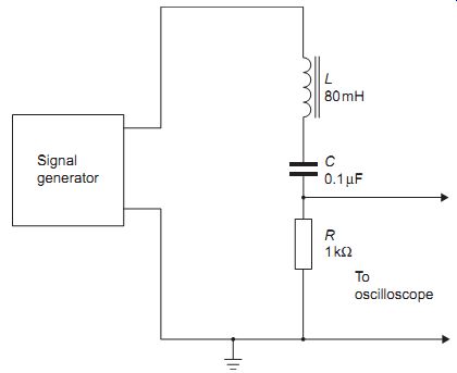
FIG. 16 Circuit for practical exercise, series resonance
In a series-resonant circuit, the current flow at resonance in the circuit will be large if the voltage across the whole circuit remains constant. Therefore, a large voltage will exist across each of the reactive components. In general, the voltage across both the capacitor and the inductor will be greater than the voltage across the whole circuit at the resonant frequency.
The ratio V_ X/V_ Z, where V_ X is the voltage across a reactor and V_ Z is the voltage across the whole circuit, is called the circuit magnification factor, symbol Q, which can be very large at the frequency of resonance.
The frequency of resonance for a series circuit can be calculated by using the formula:
f LC
_ 1 2p
where L is the inductance (henries), C the capacitance (farads), and f is the frequency (hertz).
Example: What is the resonant frequency of a circuit containing a 200 mH inductor and a 0.05 mF capacitor? Solution: Substitute the data in the equation, taking care to reduce both L and C to henries and farads, respectively.
Use L _ 200 _ 10^-3
_ 0.2 H and C _ 0.05 _ 10^-6
_ 5 _ 10- 8 F.
Take 2p as being approximately 6.3.
Then:
fr _
__
_ _ 1 63 02 5 1587 (. . ) 10 Hz 8
Find (in MHz, to two decimal places) the resonant frequency of the series combination of a 220 pF capacitor and a 15 µH inductor.
A circuit consisting of inductance, capacitance and resistance in parallel will resonate at a frequency given approximately by the same equation that was used for series resonance. However, in a practical circuit, the resistive component is more likely to be the inherent resistance of the inductor; in which case the circuit now consists of C in parallel with L plus a series resistance R that represents this component's losses. The frequency of resonance for this circuit is given by:
f LC R L
__ 1 2 1 2 2 p
If R is small, as is usually the case, the R2/L2
component can be neglected and the resonance frequency formula reverts to that for series resonance. The lossy term R2 /L2 is related to the Q factor (or quality factor, Q _ 2pfL/R) of the inductor, so that if Q is higher than about 50 the simplified formula is accurate enough for most applications.
At the frequency of resonance, a parallel resonant circuit behaves like a high value of resistance, L/CR, which is called the dynamic resistance or impedance. Again, at resonance, the phase angle between voltage and current is zero.
---------
EXPERIMENT 5
Connect the parallel resonant circuit of FIG. 17 to the signal generator. Find the frequency of resonance, which for the component values shown will be about 2250 Hz, and note that at this resonant frequency, the voltage across the resonant circuit is a maximum. Now connect another 0.047 µF capacitor in parallel with C, and note the new frequency of resonance. Remove the additional capacitor, and plot a graph of the voltage across the resonant circuit against frequency, for a range of frequencies centered about the resonant frequency. Observe the shape of the resulting curve, which is called the resonance or response curve. Now add a 10 K resistor in parallel with the resonant circuit, and plot another resonance curve, using the same frequency values. What change is there in the shape of the curve? Repeat the experiment using a 1 K resistor in place of the 10 K one, and plot all three graphs on the same scale.
---------------
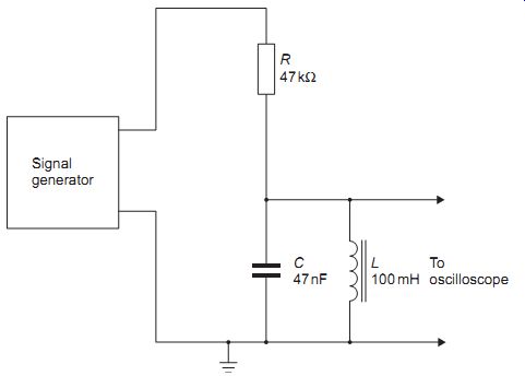
FIG. 17 Circuit for practical exercise, parallel resonance
Bandwidth
The results of these experiments will show that the addition of either capacitance or inductance to a parallel resonant circuit causes the frequency of resonance to become lower. The addition of resistance in parallel has little effect on the frequency of resonance, but a considerable effect on the shape of the resonance curve. The effect of adding a small value of resistance is to lower the peak of the resonance curve, as might be expected because the sum of two resistors in parallel is a net resistance smaller than either. In addition, however, the width of the curve is increased.
A resistor used in this way is called a damping resistor or de-Quing resistor, since it reduces the Q of the circuit. Its effect is to make the resonant circuit respond to a wider range of frequencies, but at a lower amplitude.
A damping resistor therefore increases the bandwidth of a resonant circuit, making the circuit less selective of frequency. When a parallel resonant circuit is used as the load of an amplifier, the tuned frequency is the resonant frequency of the parallel circuit, and the amount of damping resistance used will determine the bandwidth of the amplifier (FIG. 18).
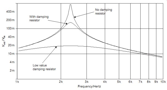
FIG. 18 Effect of adding a damping resistor to a parallel resonant
circuit
Using LCR circuits allows us to construct band-pass and band-stop filters which are more efficient than those described above. The simple LC parallel or series circuits can have resistors added to dampen the resonance so that the resonant effect is reduced but spread over a wider range of frequencies, providing a simple band-pass or band-stop action according to where the resonant circuit is placed.
For many purposes, however, these circuits do not provide a sharp enough distinction between the pass and the stop bands and much more elaborate filter circuits have to be devised. Band-pass and band-stop characteristics are often plotted on a linear scale of frequency so that the bandwidth is easier to read from the graph, but the attenuation is always plotted in terms of decibels.
Calculations on such filters are very difficult. Standard filter tables are published which reduce the design effort to scaling for the impedance and frequency, and computer programs such as SPICE can be used to graph the response for any combination of components. FIG. 19(a) shows a BPF, using a combination of series and parallel circuit to determine the band pass mid-frequency. The graph in FIG. 19(b) shows the response of this circuit for the component values shown. It should be noted that there is significant insertion loss and ripple in the pass band. The ripple and losses can be minimized by careful design taking account of factors like the d.c. resistance of the inductors and tolerance of all the components, but this is beyond the scope of this guide.
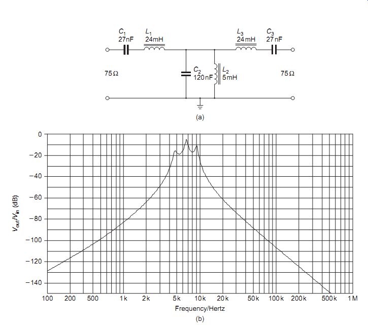
FIG. 19 (a) Circuit, and (b) computed response curve for a band-pass
filter
QUIZ
1. In a series circuit made from a resistor and a capacitor the voltage across the resistor is 100 V and the total circuit voltage is 141.4 V. What is the voltage across the capacitor?
(a) 50 V
(b) 75 V
(c) 100 V
(d) 150 V.
2 In the circuit in question 1 the current is 1A. What is the value of the resistor?
(a) 1 O
(b) 10 O
(c) 100 O
(d) 1000 O.
3 In the circuit in question 1 the current is 1 A. What is the value of the capacitor if the source frequency is 50 Hz?
(a) 16 µF
(b) 32 µF
(c) 64 µF
(d) 100 µF.
4 An RC low-pass filter uses a 47 kO resistor and a 33 nF capacitor. What is the frequency at which the output voltage is _3 dB relative to the input?
(a) 97.4 kHz
(b) 645 kHz
(c) 103 kHz
(d) 155.1 kHz.
5. A parallel circuit consisting of a variable capacitor and a 160 µH coil is used in a radio receiver to select a station whose frequency is 1215 kHz. What value will the variable capacitor have when the station is correctly tuned?
(a) 75.9 pF
(b) 107.2 pF
(c) 151.8 pF
(d) 300 pF.