Thermocouple simplifies temperature controller
By V. J. H. Chiu National Research Council, Division of Chemistry, Ottawa, Canada
Virtually all the designs for low-noise, high-temperature controllers of the type that use zero-crossing switches have thermistors in the sensing circuit--an impractical configuration in many cases because of the size requirements and availability of the thermistor itself. To over come these inconveniences, this simple circuit substitutes an ordinary thermocouple for the thermistor, yet works as well as a thermistor-based one-for instance, it controls the environmental (furnace) temperature from room temperature to 1,100°C to within ± 2%.
In general operation, the furnace is heated from the ac line through a triac, triac driver A1, and the CA3079 zero-voltage switch A2. The CA3079, in turn, switches on when the output differential from the thermocouple drops below a value corresponding to a given furnace temperature. Switching occurs because the amplified thermocouple voltage, VT, at the output of A3 falls below the user-preset reference potential, VR, at the input to A4. Note that in addition, the CA3079 must be biased so that potential V13 is initially less than the comparator's output, V9, in order that the circuit containing RL of the furnace will be completed and current will flow when the furnace is cold.
The thermocouple voltage is linearly proportional over its entire range to the temperature in the furnace; consequently, if potentiometer R1 is linear, it can be directly calibrated in terms of temperature. For optimum switching, the voltage V13 should be set at half of the LM324's supply voltage.
As for cost, the prototype circuit was built for an outlay of less than $20.
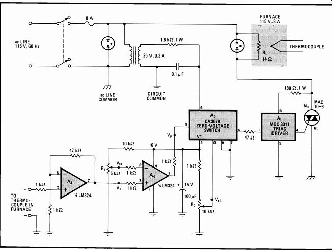
--------------- Hot-wired heater. Chromel-Alumel thermocouple eases
design of zero-crossing-switched temperature controllers. Potentiometers
R,-R2 set the reference voltage for switching on furnace from CA3079
switch without the need for setting up a complicated reference scheme.
Linear response makes it easy to calibrate R, as a direct function of
desired temperature. Circuit works to 1,100°C, is accurate to within
± 2%.
Lamp dimmer fades in equiluminous steps
by Mark E. Patton Sanders Associates, Nashua, N. H.
This programmable light dimmer will serve particularly well as an intensity-control source for vision response testing and in theatrical lighting systems, where it can provide, as perceived by the human eye, a virtually linearly stepped increase or decrease in luminous output (the Munsell curve).' Using readily available chips, it can be built for less than $20.
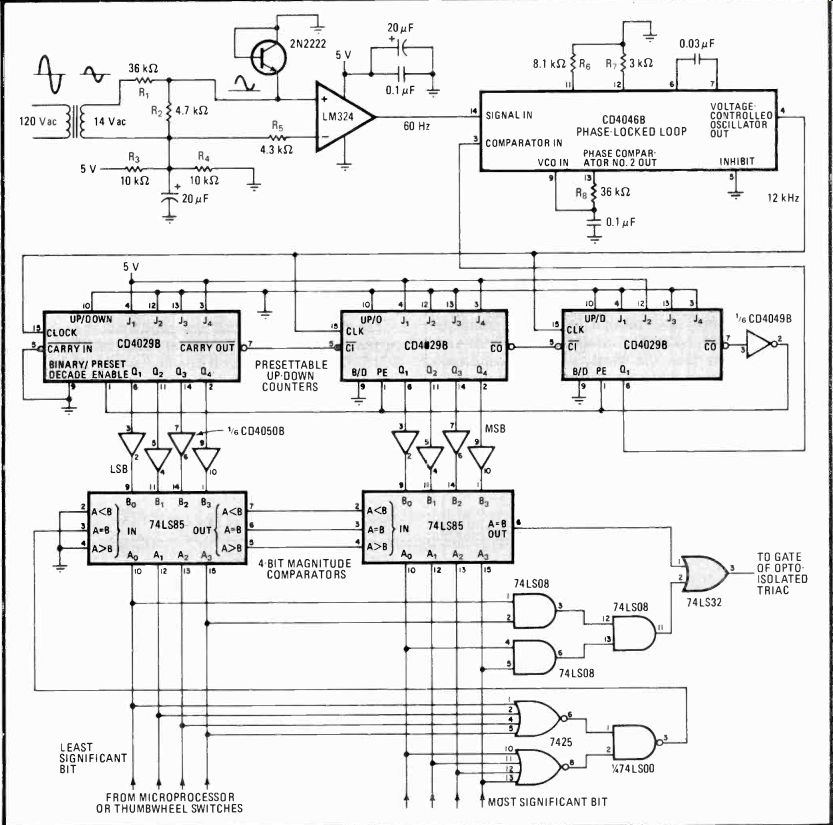
-------- Linear lighting. Programmable lamp dimmer can provide intensity
increments and decrements in near-linear steps (as perceived by human
eye), virtually meeting Munsell curve specifications. BCD control word,
derived from microprocessor, sets switching point on 80-Hz line input.
In operation, a triac-driven lamp is triggered by the 60-hertz line input once during each half cycle, at a point determined by an eight-input binary-coded decimal control word derived from a microprocessor or a thumb-wheel switch. Thus the lamp brightness may be easily selected and accurately maintained, or alternatively, it can be gradually diminished or increased as desired.
As shown, the LM324, biased to operate from a 5-volt dc supply, works as a comparator to provide 60-Hz square-wave pulses to the CD4046 phase-locked loop and as a buffer to suppress line transients. The PLL and the 4029 up-down counters working together act to multiply the line input by 200, so that the counters decrement from 99 toward 0 at a 12-kilohertz rate. This rate permits the selection of 12,000/(60 x 2) = 100 brightness levels.
Meanwhile the two-digit BCD control word is introduced to the 74LS85 4-bit magnitude comparators, where it is compared with the output of the counters.
When the line-synchronized output of the counter becomes equal to the control word, the opto-isolated triac, which is connected to the ac line, is fired.
The triac should be heavily filtered to prevent switching noise on the line from reaching the logic circuitry.
Also, to increase circuit stability near the zero and maximum-voltage switching points of the 60-Hz input signal, the outputs of the 74LS85s are gated for a loaded BCD code of 99 and are disabled for a code of 0.
References
- GTE Sylvania, GTE Sylvania Lighting Handbook, 5th ed., 1974.
Zero-crossing controller heats beakers noiselessly
by Gerald D. Clubine East Texas State University, Fine Instruments Shop, Commerce, Texas
Present-day low-cost heater/dimmer controls of the type used to warm the contents of laboratory beakers and flasks are primarily modeled after the hot-plate burners in electric stoves. Consequently, they feature thermal switches that generate unwanted electronic hash and noise spikes because of the make-and-break operation of the device under a varying thermal load. This circuit controls heat by varying the duty cycle of the heater coil-but it switches the coil on and off during the zero crossings of the 115-volt ac power line, thus eliminating all types of noise. In addition to offering solid-state reliability, it costs no more than the old hot plate. And it is far less costly than the widely used but unnecessary closed-loop controls that use a sensing element.
The heart of the circuit is the CA3059 zero-crossing trigger, At, which controls the solid-state switch, triac Q2. As shown, the ramp output of the unijunction oscillator Q1 is applied to the on/off sensing amplifier at pin 9. The ramp has a peak amplitude of 2/3 Vc and a time constant of R7C3, which is long compared with the 60-hertz line rate but relatively short with respect to the thermal response time of the hot plate.
A user-set reference voltage is applied to the other input of the sensing amplifier at pin 13. Potentiometer R2 thus sets the temperature by control of the duty cycle, for when \ire' is greater than the instantaneous ramp voltage, A1 and Q2 are turned off, and vice versa. Note that the control calibration will be linear to the degree that the ramp voltage is linear. Power is applied to the heater coil during the zero crossings of the line input and removed during these times, too; as a result, switching is achieved at the zero power level, and no noise can be generated.
The choice of the triac will depend upon the amount of current required by the heater coil. In this case, a SC has been used, as the heater coil demand was only 6 amperes.
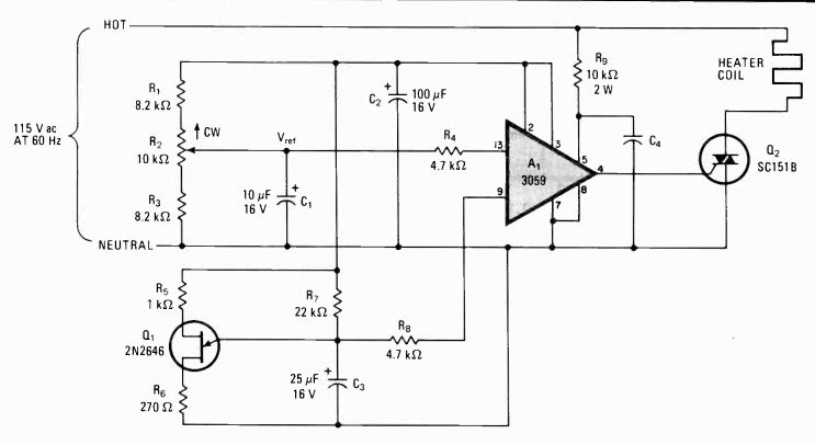
-- Selective radiator. A triac fired by this controller applies power
to and removes power from heater coil of hot plate during zero crossings
of the 115-V ac power line, thus eliminating unwanted electrical hash
and noise formerly caused by mechanical-type thermal switches. User sets
temperature with duty-cycle control F12, which turns on A, and triac
when V,e, is less than the instantaneous ramp output of oscillator Q,.
One-chip tachometer simplifies motor controller
by Henrique Sarmento Malvar Department of Electrical Engineering, University of Brazilia, Brazil
Setting and stabilizing the angular velocity of a dc motor by means of a charge pump and a servo-amplifier, one-chip tachometers such as National Semiconductor's LM2917 serve well as a simple but elegant motor-speed controller. Such an arrangement is preferable to the widely used scheme in which both positive and negative feedback is utilized to keep the motor's back electromotive force, and thus its speed, constant by generating a voltage that is proportional to a given load.
As shown in the figure, a magnetic pickup coil detects the angular velocity of a motor-driven flywheel and feeds the low-amplitude pulses, whose frequency is proportion al to the motor speed, to the LM2917's charge pump. As a result, the pump generates a current, II, whose average value is directly proportional to the input frequency.
The operational amplifier that follows compares this voltage to a user-set reference and, through power transistor Q1, generates a voltage for the motor's armature of VA = (R2/R1)(Vrei- I1R1). Thus, potentiometer R6 sets the motor's speed, for when V1 . V,er, voltage VA decreases, and vice versa.
In this application, the gain of the operational amplifier, determined by resistors R1 and R2, has been set at approximately 150. The greater the gain, the lower the variation of motor speed with changes in load resistance. However, the setting of very high gains should be avoided, because there will be a reduction in the gain and phase margins-that is to say, a loss of stability in the feedback control loop.
As for the selection of other components to meet any particular application, note that capacitor C1 serves a double purpose: it integrates pulsed current II, thereby performing a smoothing function, and it sets a low-frequency pole for the amplifier, thereby ensuring stability. C2 sets the conversion factor of the tachometer and should be increased for low-speed motors. R3 minimizes the offset due to the amplifier's bias currents at pins 4 and 10. Finally, C3 functions as a noise filter.
As seen, the LM2917's tachometer conversion factor will be almost independent of its supply voltage, as a consequence of the zener diode connected at the device's supply port. The supply voltage should not fall outside the range of 10 to 15 volts, however.

----- Setting speed. LM2917J tachometer, which is basically a frequency-to-voltage
converter, sets and stabilizes motor speed. Few RC components are required,
thereby simplifying circuitry. Power transistor Q1 is the only external
active element needed.
On/off timer maintains precision over wide range
by Alfred C. Plnchak, Cleveland Metropolitan General Hospital, Department of Anesthesiology, Cleveland, Ohio
This circuit improves in several ways upon available designs for timers whose on and off periods are selectable. Specifically, it provides more precise control of those periods, a wider range over which the time base can be set, and a more flexible range that the supply potentials may assume. The circuit, which if implemented mostly in complementary-mos, draws a maximum of 20 milliamperes at 5 volts, including relay power.
As shown, the HD4702 bit-rate generators, A1 and A2, provide a crystal-controlled clock signal for the ICM7240 timer-counter chips, A3-A6. Clock periods of from approximately 100 microseconds to 4 seconds are ordered by AI and A2. The timer-counter outputs are wire-ORed together and are weighted in a binary fashion, with each position increasing in a 1, 2, 4, . . . 32,768 sequence. Thus by adjusting each dip switch appropriately, the on and off periods of the output signal can be independently set over the range Tc-c T.<65,536Tc, where T6 is the clock period and T. = Toff.
A3 and A4 form a one-shot that determines the off (low) period. Similarly, one-shot pair AS sets the on (high) period. Because the output of each one-shot (points A and B) are tied back to its own reset terminal and also to the trigger port of the other one-shot pair, the output at A is inverted with respect to B.
The 4702 time-base generators provide a direct clock signal for A3 and AS, with A4 and A6 driven by pins 8 of A3 and A5, respectively. A3 and As, through transistors Q1 and Q2, also are part of the wired-OR network. Thus, all portions of each timer chip can be utilized to set the high and low periods. This feature is in contrast to previously published designs that cascade 2240 timers but restrict the Toff time to an integral multiple of 128TH.
Unfortunately, because of the wired-OR arrangement, the amplitude of the output signals at points A and B does not increase proportionally with supply voltage. In order to increase the effective range of the supply voltage, Q3 is added to provide a level-shifting function. This extends the maximum supply voltage range from approximately 5.5 to 12 v.
The minimum supply voltage for an electronic output is approximately 3.8 v. However, the actual minimum voltage in cases where a relay is used will depend on the particular relay chosen. In this case, the minimum sup ply voltage was about 4.6 v.
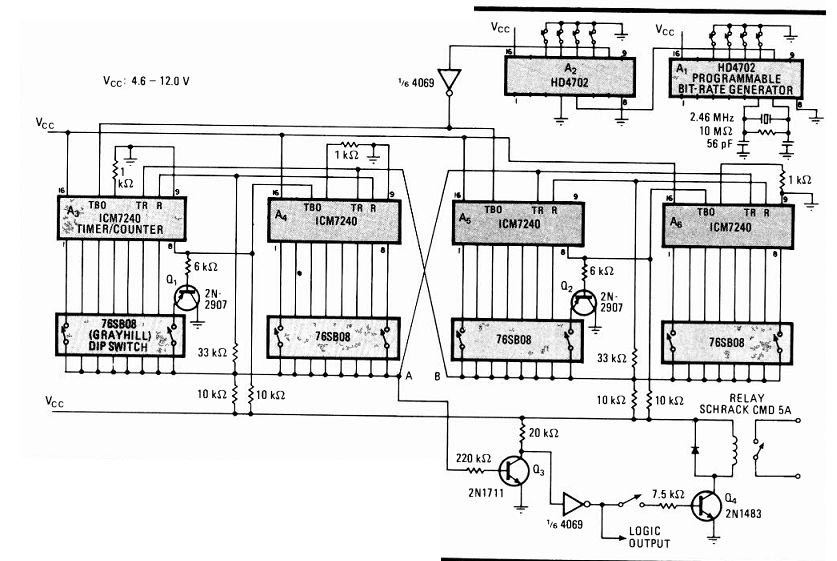
----- Improved. Timer, generating clock intervals ranging from 100
A is to 70 hours, allows for individual setting of on and off times in
100-µs-to-4-second steps over entire range. Level-shifting transistor,
03, ensures that output amplitude of wired-OR network is proportional
to supply voltage. Device draws a maximum of 20 mA at 5 V.
Voltage-controlled resistance switches over preset limits
by Chris Tocci Halifax, Mass.
Using two field-effect transistors as switches, this voltage-controlled resistor network can order up any value of resistance between two preselected limits. It is unlike other circuits in that it does not employ the drain-
to-source resistance of matched FETs, whose Rd, characteristics are usually proportional to a control voltage. As for circuit linearity, it will far exceed that of convention al networks using a single FET in various feedback configurations.' In operation, oscillator A1-A2 generates a 0-to-10-volt triangle wave at 100 kilohertz, which is then compared with the control signal, V at A3. During the time that the control exceeds switching voltage VT, FET Q, is turned on, and resistor R, is placed across resistance Rout (disregarding the Rd, of Q1). At all other times, FET Q2 is on and resistor R2 is placed across Rm. Thus Rout is equal to an average value proportional to the time each resistor is placed across the output terminals, with the actual resistance given by R55t = (R,- R2)V,/10 + R2, for R1 >R2. This relationship will hold provided any potential applied to the Rest port from an external device is less in magnitude than the supply voltages; that any signal processing at R., be done at a frequency at least one decade below the 100-kHz switching frequency; and. that the upper and lower resistance limits, R, and R2, are much greater than the on-resistance of Q1 and Q2, respectively.
Potentiometer R1, adjusts the baseline of VT to zero so that with V, = 0, Rotun = R2, where n is a constant.
Further calibration can be carried out by trimming R, and R2 to precise values.
This circuit is readily adapted to many applications, such as a one-quadrant multiplier. This is achieved by connecting a voltage-controlled current source into the R,, port to build a dc-shift amplitude modulator whose carrier frequency is the switching frequency. The audio information or data is taken from V5, but with the signal offset by 5 volts. Thus the dynamic range of the circuit will be 10 v.
References
1. Thomas L. Clarke, "FET pair and op amp linearize voltage-controlled resistor," Electronics, April 28, 1977, p. 111.
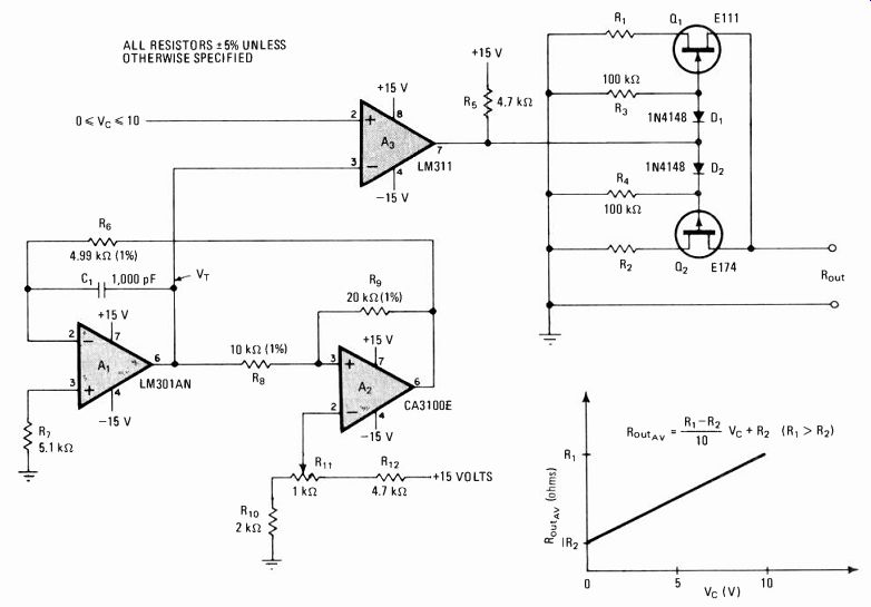
----- Ohmic linearization. FET switches in voltage-controlled resistor
network place maximum-minimum resistors R1 and R2 across Roo, so that
the resistance is proportional to the average time each Is across output
port. Switching technique ensures piecewise-linear operation. This circuit
lends itself to many applications, such as a-m modulator, by placing
voltage-controlled current source across Rout.
Divider sets tuning limits of C-MOS oscillator
by Henno Normet Diversified Electronics Inc., Leesburg, Fla.
Useful as it is, the square-wave RC oscillator implemented in complementary-mos has one shortcoming setting its maximum and minimum frequencies of oscillation independently while also maintaining accuracy is extremely difficult. By placing a voltage divider in the feedback loop of the conventional three-gate circuit, however, a one-time trimming adjustment can accurate ly set the maximum and minimum frequency excursion and will force the ratio of the upper to the lower limit of oscillation to approach a value virtually determined by the resistors used in the same divider.
The standard RC oscillator generates a frequency of f r-t10.482/R1C, where R1 = R2, as shown in (a). Gener ally, it is not practical or economical to use a variable capacitor for C. A potentiometer could be substituted for R1 to tune the frequency, but slight differences in inte grated-circuit parameters will preclude predicting the maximum and minimum frequencies of oscillation with any degree of accuracy for a particular chip. The only other method for setting the upper and lower frequency limits is to parallel several capacitors across C, a tedious procedure at best.
Alternatively, R1 can be a potentiometer that is placed virtually in parallel with voltage divider Ra-R5 through C (b). In this way, capacitor C is no longer charged from the fixed-voltage output of the middle gate in (a), but from the voltage divider across the output. R1 is thus used to change the circuit's time constant without affecting the potential that is applied to C.
The upper and lower limits of oscillation are deter mined by the position of R4's wiper arm and by the values of R4 and R5. With the tap at point A, the circuit will oscillate at a frequency given by f = 1/2.2R IC.
With the wiper at point B, the frequency will be f = 1/1.39RIC. The frequency ratio to be expected is thus 2.2/1.39 = 1.6. The actual frequency change measured with the particular chip used for breadboarding was 56%, which is thus very close to the intended value. The ratio will increase as R4 is made larger with respect to Rs.
The circuit has only one small disadvantage--the load presented by R4 and R5 does increase the power-supply drain by approximately 0.5 milliampere.
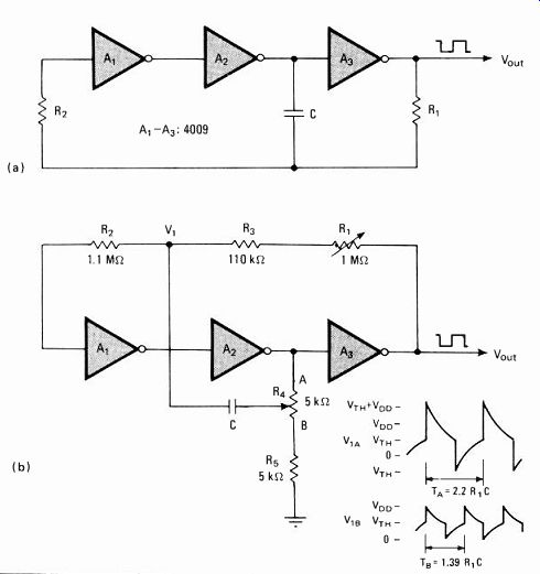
--- Calibrate. IC anomalies, inherent circuit imbalance, and the
expense of making C variable preclude setting upper and lower oscillation
limits of typical RC oscillator (a) with any accuracy. Placing R, virtually
in parallel with voltage divider (b) through C gives circuit one-knob
frequency control, with upper-to-lower oscillation ratio in effect determined
by R. and R5.
Multiplier increases resolution of standard shaft encoders
by Frank Amthor School of Optometry, University of Alabama, Birmingham
The resolution that can be attained by two-channel shaft encoders of the type used in speed controllers and optical-positioning devices may be increased by employing a digital frequency multiplier to derive a proportionally greater number of pulses from its TTL-compatible outputs. In this way, an up/down counter, which is normally driven by the encoder in these applications, can position the shaft more accurately and is more responsive to changes in speed and direction. Only two one-shot multivibrators and several logic gates are needed for the multiplier circuitry.
The circuit works well with a typical encoder such as the Digipot (manufactured by Sensor Technology Inc., Chatsworth, Calif.). In this case, the 128 square waves that are generated per channel for each shaft revolution (with output from the other channel in quadrature) are transformed to 512 bits per cycle.
When the shaft rotates in a clockwise direction, the output from port A of the encoder always leads the output from port B by 90°, and the logic will generate pulses only to the up input of the counter on both edges of both channel outputs. Thus, four pulses per square wave are generated. Rotation speed is limited by the duration time of the positive-edge-triggered one-shots, which should be kept to a few microseconds or less. Note that both the count-up and the count-down inputs of the counter are normally held high.
On the other hand, when the shaft's rotation is in a counterclockwise direction, the output of B leads that of A by 90°. In this case, four pulses per square wave are presented to the down input of the counter.
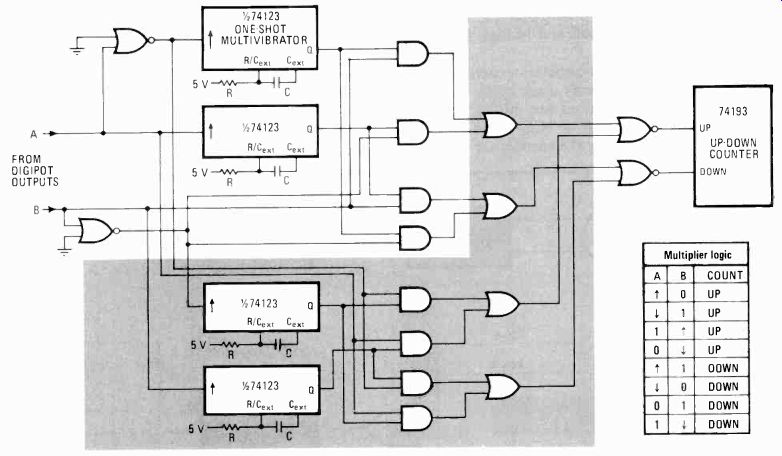
------51 Increments. Pulse multiplier yields 512 count-up or-down bits
for 128 square-wave cycles (one revolution) from two-channel shaft encoder,
for more resolution in speed controllers and optical positioning systems.
Eliminating tinted area yields 256 bits per revolution.
Simplified multiplier improves standard shaft encoder
by Michael M. Butler Minneapolis, Minn.
The pulse multiplier proposed by Amthor [Electronics, Sept. 11, p. 139] for increasing the resolution of a standard shaft encoder may be simplified, and improved as well, with this low-power circuit. Using only three complementary-mos chips to derive a proportionally greater number of pulses from the encoder's output for a positioning up/down counter, it is relatively insensitive to encoder phase errors, uses no temperamental one-shots, and can detect the occurrence of illegal transition states generated by the encoder or circuit. It will serve well in electrically noisy industrial environments.
As in Amthor's circuit, the multiplier (a) used to drive the counter produces four pulses for each square-wave input of the two-phase encoder, whose outputs are displaced 90° with respect to one another. In this circuit, however, two 4-bit shift registers, three exclusive-oR gates, and an eight-channel multiplexer (b) derive the pulses. Previously four one-shots and 16 logic gates were required for the same task.
As seen, the clocked shift registers generate a 4-bit code to the multiplexer for each clock cycle. To ensure that no shaft-encoder transitions are missed, the clock frequency should be at least 8 NS, where N is the number of pulses produced by the encoder for each shaft revolution and S is the maximum speed, in revolutions per second, to be expected. A clock frequency of 1 megahertz or less is recommended for optimum circuit operation.
The code is symmetrical, and so only three exclusive OR gates are required to fold the data into 3 bits. These bits are then applied to the control ports of the three input multiplexer, which will generate the truth table shown.
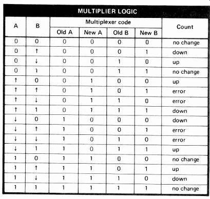
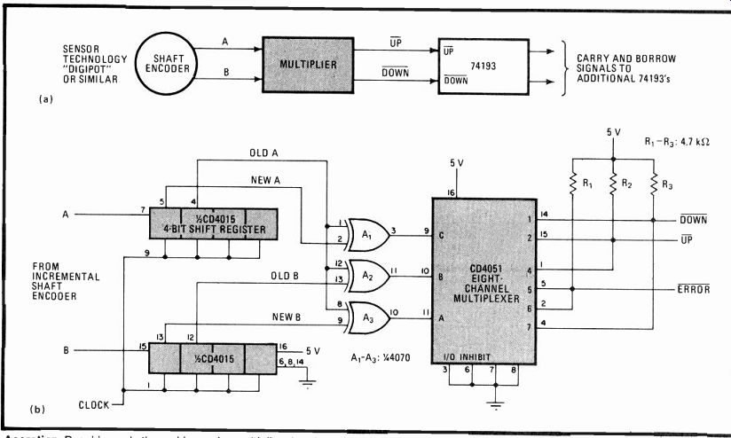
--- Accretion. Requiring only three chips, pulse multiplier
gives better resolution to optical positioning systems that are driven
by a shaft encoder. Low-power circuit is relatively insensitive to encoder
phase errors. Stability is high because no one-shot multivibrators are used.
Fewer parts resolve shaft encoder data
by Bill McClelland Digicomp, Darien, Conn.
This circuit achieves the same resolution as the circuit proposed by Amthor [Electronics, Sept. 11, 1980, p. 139] but requires only one integrated circuit, instead of seven, and half the number of discrete components.
A standard shaft encoder has two ports, A and B, each generating a square wave as the shaft encoder is turned.
The square wave from port A will either lead or follow port B's square wave by 90°, depending on the direction of the rotation of the encoder (a).
To get the maximum resolution out of the shaft encoder, every change of state for both A and B must be counted. Depending on the direction of rotation of the shaft encoder, the counter will count up or down. By exclusive-NOR-ing square waves A and B at gate Az, a square wave that changes state whenever there is a change of state of either A or B can be obtained. The output of exclusive-NOR gate A3 is high except when a change of state at gate A2 occurs. Whenever the output of gate A2 changes state, the two inputs of gate A3 will be of opposite state for a time determined by R2 and C2, generating a short, low-going pulse. By using complementary-mos exclusive-NOR gates, the pulse at the output of gate A3 will have about the same duration for both the positive and negative transitions of gate A2. The trailing edge of this pulse is used to clock the counter, allowing setup time for the up-down control (b).
The up-down control is generated by R1, C1, and gate A,. R, and C, act as a latch, holding the value of B prior to a change of state of A or B during the clock pulse at gate A3. Exclusive-NOR-ing the value of A just after a change of state in A or B, with the value of B set just prior to a change of state of A or B, achieves the proper up-down control.
The operation of gate 1 can be demonstrated as follows: square waves A and B are out of phase with each other by 90°. Adding - 90° to B would change the phase shift to 0° or - 180°, depending on the direction of rotation of the shaft encoder.
As a result, the output of exclusive-NOR gate AI would be high when A and B are in phase and low when A and B are 180° out of phase. Since the only concern is the output of gate AI when the counter is clocked, R, and C1 give enough time lag to phase-shift B for the duration of the clock pulse at gate A3. For this reason the time constant R/C, is greater than R2C2.
The polarity of the up-down control may be inverted by swapping the A and B wires or by using the fourth exclusive-NOR gate in the 4077 integrated circuit as a selectable inverter-buffer. If the clock signal needs to be inverted for another type of counter, the entire 4077 exclusive-NOR-gate package can be changed to a 4070 exclusive-oR package. If standard c-mos rise and fall times at the A and B inputs cannot be guaranteed, it becomes necessary to buffer the A and B inputs with Schmitt trigger, such as a 74C914.

Resolved. A shaft encoder output, shown as pulse trains A and B, is
split into clocking and control signals for driving a counter (a). Any
transition in either of the encoder outputs results in a clocking pulse
to the counter, while the sequence of the encoder outputs deter mines
whether the count is up or down (b).
Train speed controller ignores track resistance
by Stephen H. Burns U. S. Naval Academy, Electrical Engineering Department, Annapolis, Md.
Because it keeps the voltage applied to any universal motor constant and independent of line resistance for a given line voltage, this circuit will be especially attractive for use with model trains, for which it will maintain speed independently of the resistive joints in the tracks.
No modification of the speed-controlling transformer used with the trains is required.
This circuit rides within or near the locomotive and is inserted in the electrical path between the motor and the track pickup and return. Thus it is necessary to connect the ac input of this circuit to the track pickup and frame of the locomotive and to connect the dc output of the circuit across the motor windings. This way the circuit develops a constant average voltage across the motor for a given transformer setting.
This is accomplished with a four-section circuit, with block A containing the supply for powering the unit.
Blocks B and C derive a gate pulse inversely proportional to the magnitude of the input voltage and a control voltage proportional to the input signal so that motor speed can be set. Block D handles the power-switching function.

---------- Rail tamer. Controller keeps driving voltage to model
trains independent of the resistance in the track joints. Output voltage
is derived from pulses whose widths are inversely proportional to the
ac input, generated at zero crossings so that load variations on the
line are disregarded. Timing diagram details the operation.
Diode bridge 111, diodes D1 and D2, capacitor C1, and Norton amplifier AI constitute block A, which is actually a three-stage supply. B: provides full-wave rectified dc for power stage Q3 and DI and C1 extract and filter power for A1-A4. Zener diode D2 and A1 provide a regulated 5 volts for current source Q1 and to establish a switching reference voltage for amplifier A2.
In operation, B1 and Q3 electrically disconnect the motor from the power source near each zero crossing of the ac input. At this time, a pulse is developed at the output of A2, its width equal to P = 2V,/wV,, where V, is the switching reference voltage, w is 120 pi radians/sec, and V, is the input voltage (see timing diagram). Note that by sampling near the zero crossings, the width of the pulse is made independent of the load on the ac line. One sense diode, D3 or D4, reference diodes D5 and D6, and one bridge diode set the switching threshold, V,. This reference voltage is thus equal to four diode drops, or approximately 2V.
A3, Q1, and Q2 develop from the pulse a control voltage, Vc, whose average value can be expressed as Vc = irIoRV,/(2V,). A3 and Q1 constitute a 0.3-milliampere (10 constant-current source. A total resistance of 52 megohms placed in series between Vcc and the inverting input of A3 was found best to compensate for changes in Lo versus supply variations.
The power switching stage includes feedback capacitor C3, amplifier A4, isolation diode D7, damper diode D8, and Q3. C2 and C3 were selected so that Q3 switches efficiently under all load conditions. Smaller values of C2 result in more efficient switching but increase output resistance. Larger values of C3 will result in greater overshooting in response to a transient.
With a source voltage of from 7 to 25 v rms and a load of 10 ohms, the circuit will generate an output of from 3 to 12 v. Increasing the line resistance from 0 to 4 C1 will cause a typical change in output voltage of only 0.1 v for a line drop of several volts.
Power-up relays prevent meter from pinning
by Michael Bozoian Ann Arbor, Mich.
Sensitive micro-ammeters with d'Arsonval movements are still manufactured and used widely today, but surprisingly, there has been little attempt to correct one defect in their design-they are still very prone to pointer damage from input-signal overload and turn-on/turn off transients. Although ways of protecting the meter movement from input signals of excessive magnitude are well known and universally applied, no convenient means of preventing the pointer from slamming against the full-scale stop during power-up or power-off conditions has so far been introduced or suggested in the literature. However, the problem may be easily solved by the use of a 555 timer and two relays to place a protective shunt across the meter during these periods.
Basically, the 555 timer closes reed relay A's normally open contacts on power up and puts shunt resistor R across the meter for 5 or 6 seconds until the turn-on transients have subsided, as shown in the figure. The normally closed contacts of relay B are also opened at this time.
On power-down, relay B reintroduces the shunt to protect the meter from turn-off transients. Such a scheme is more effective than placing a diode across the meter, as is often done and is much more elegant and less bothersome than manually activating an auxiliary mechanical switch for placing R across the meter each time it is used.
R has been selected for a meter movement having a full-scale output of 200 microamperes and an internal resistance of 1,400 ohms. The complete circuit may be mounted on a 2-by-21A-inch printed-circuit board. The only design precaution is to ensure that relay B is energized from a source that has a fast decay time during power-off conditions. Here, the voltage has been tapped from the meter's power-supply rectifier.
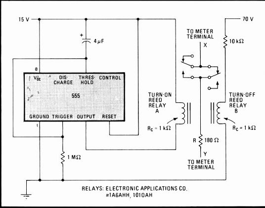
--Shunted. Reed relays and 555 timer prevent d'Arsonval movement
from slamming against microammeter's full-scale stop during power-up
and power-down conditions by introducing shunt resistor across meter
terminals until transients die out. Method does not degrade meter's accuracy
or its transient response to input signals.
Opto-isolated line monitor provides fail-safe control
by Eric G. Breeze and Earl V. Cole General Instrument Corp., Optoelectronics Division, Palo Alto, Calif.
Because of the degree of isolation they provide, optically coupled ac-line monitors serve well as a small, reliable low-power interface in ac-to-dc control applications, where status information of the ac line is crucial. When a type is used that is TTL- and microprocessor-compatible-like the MID400, which performs the basic monitoring function on a single chip-a circuit can be built that ensures fail-safe control under the most difficult monitoring assignments. And when combined with a 555 timer, the monitor will have improved drive capability, more precise control of the turn-on and turn-off delay times, and better noise immunity than units that are typically available.
As shown in Fig. 1, two gallium arsenide infrared light-emitting diodes connected back to back and optically coupled to an integrated photodiode and high-gain amplifier make up the MID400, which is encased in an eight-pin dual in-line package. In operation, each LED conducts on alternate half cycles of the ac-input wave form, together producing 120 pulses of light per second.
Thus the photodiode periodically conducts, causing the amplifier to drive the npn transistor at the output to its on state. As the amplifier's switching time has been designed to be slow, it will not respond to an absence of input voltage lasting a few milliseconds; therefore it will not respond to the short zero-crossing period that occurs each half cycle.
The MID400 operates in one of two basic modes: saturated or unsaturated. It operates in the saturated mode when the input signal is above the minimum required current of 4 milliamperes root mean square and the photodiode pulses keep the output of the MID400 low. It operates in the unsaturated mode if the input current drops below 4 mA rms. Under these conditions, a train of pulses will appear at the output. In this way, a clean clock generator, devoid of power-line transients because it is isolated, may be realized.
If the input current drops below 0.15 mA, the device turns off. This causes the output of the MID400 to remain high.
Adding an external capacitor, C, to pin 7 of the device produces a time-delay circuit. The amount of delay on power-up is short because the photodiode has a low impedance when conducting. When ac is removed, however, the delay is long because the capacitor must discharge through the leakage resistance of the amplifier and photodiode. The larger the capacitor, the longer the delay.

--- 1. Control chip. Opto-isolated power-line monitor on single IC
provides hash-free driving signals for ac-to-dc control applications.
When united with 555 timer, circuit provides precise control of on and
off delay times, improved driving capability, and good noise immunity.
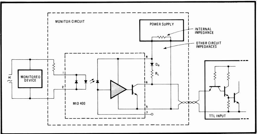
---- 2. Immune. Monitor is easily modified for fail-safe control tasks,
such as are required in industrial applications. Diode prevents component
failures from creating output glitches. MID400's output circuit design
inherently prevents generation of glitches caused by supply anomalies.
In lieu of capacitor C, the use of a 555 timer also provides pulse shaping by yielding faster rise and fall times at the output. Here, the 555 is used as a Schmitt trigger with well-defined thresholds, the high state being 2/3 v., and the low state being 1/3 V. Besides providing noise immunity, use of the 555 also minimizes oscillations that might occur if a TTL device were to drive a minicomputer.
Timing elements Rx and Cx set the delay. With appropriate choice of the time constant, the circuit can be made to respond to, or to ignore, one or more ac input cycles. Diode Dx permits the fast charge and slow discharge of Cx or, if the diode's polarity is reversed, the slow charge and fast discharge of the capacitor. The actual delay time will depend on the operating mode of the MID400.
For industrial, military, or medical applications in which fail-safe operation is important, the circuit's response must also be considered for the cases where either the ac input or the MID400 supply is removed.
Fortunately, the MID400 has been designed so that its output transistor is on (low) only when both the ac input voltage and the supply voltage are present, thus simplifying the problem of providing a valid fail-safe control signal. Consider the case where the MID400 is powered by a separate 5-volt supply and the monitor drives a TTL-compatible interface through a twisted-pair line (Fig. 2). Normally, the inherent truth table of the device will prevent an erroneous output to the TTL interface circuit. Should RL fall below 1 kilohm for one reason or another, however, and the power supply be off, the TTL input of the minicomputer will appear low because of excessive current flow through RL. Diode Da in series with RL blocks any reverse current, eliminating the problem.
Stepper resolves motor's angular position to 0.1°
by Jaykumar Sethuram Electronic Associates inc., West Long Branch, N. J.
One-chip digital comparators and counters simplify the design of this controller, which resolves the position of a stepping motor to 0.1°. Using complementary-MOS circuitry, the unit is low in cost and power consumption is minimal.
The set of four binary-coded decimal numbers, D1 to D4, introduced to the cascaded 40085 4-bit comparators, are the command signals that order the motor to the desired bearing expressed in hundreds, tens, units, or tenths of a degree, respectively. The range of the input set is thus 0000 to 3600. With the aid of the comparators and sequential logic, the 40192 up/down counters track the position of the stepper at every instant, updating its count and thus rotating the motor until its contents match the setting of D1-D4.
As can be seen, the sequential logic circuitry deter mines the direction of rotation of the stepper and counter by monitoring the A = B, A> B, and A <B outputs of the output comparator. The logic is designed to rotate the stepper from its current position to the desired position in the minimum number of steps. Thus, if the motor's present position is at 5° and the intended position is 300°, the stepper will automatically be rotated in a counterclockwise direction.
The circuit can be easily modified for applications where the input data is available for only a very short time. In such cases, it is only necessary to add input latches to capture the data.
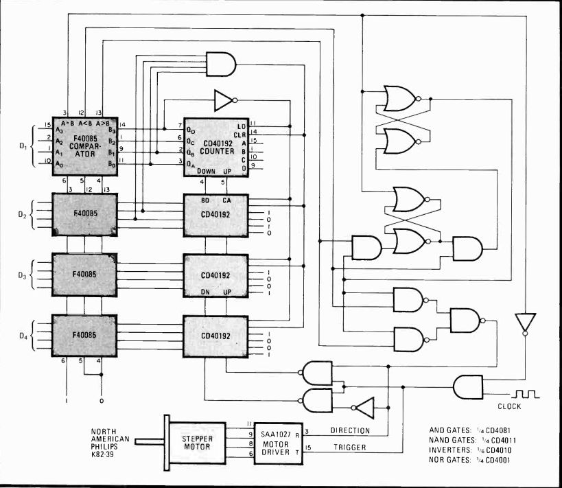
--------- Move a bit. Stepping motor is rotated into desired position
with comparators and sequential logic that minimizes the difference between
the 4-bit command set D,-D., and the output of the up/down position-tracking
counter. Angular position is resolved to 0.1°.
Serial-data interface eases remote use of terminal keyboard
by Robert Nixon Nixon Engineering Co., San Jose, Calif.
A keyboard that can be detached and operated at a distance from its terminal is often desirable in a computer-based system, but the job of developing the proper cable and connector can be hard and time-consuming.
The interconnecting wire count can be reduced to just two leads, however. The trick is to choose a keyboard that generates a serial output for each keystroke and use it with the current-modulating interface shown. A minor modification will adapt the circuit to the RS-232 bus.
Here, the microprocessor-based keyboard is the Micro Switch 103SD24-2, which delivers the serial ASCII data at 110 bits per second. Power to the keyboard, which requires only 5 volts, is provided by the 12A7812 voltage regulator. This device also serves as a current limiter, protecting the interface against damage caused by shorts in the connecting cable. A second regulator, the µA.7805, smoothes out the small variations in voltage generated by the current modulator.
During the mark states of the data stream, transistor Q, is held off because the keyboard output is active-the total current through R1 and the keyboard is 360 milli amperes, which represents the difference between the supply voltage and the keyboard's optocoupler output stage. During the space interval of the serial data stream, the keyboard output is inactive, and Q1 is turned on. The total supply current then becomes 610 ITIA.
Diodes D1 and D2 allow for the small voltage drop between the Darlington-coupled output of the keyboard, ensuring that Q, is switched properly. Capacitors C1 and C2 aid in stabilizing the ALA7805 regulator during modulation.
The two-state current variation is detected on the receiver side by Q2, and associated resistors R3-R5.
During the mark state, the drop across R3 is about 550 millivolts, which is not enough to turn on the transistor.
During the space state, however, the additional current produced will switch on Q2 and generate a positive voltage level at the output. Note that R4 and R5 prevent the transistor from being damaged by a short circuit.
For TTL compatibility, the output signal should be introduced to a Schmitt trigger to eliminate hash and ill-defined switching levels. To interface with the RS-232 bus, it is only necessary to increase R7's value to 3 kilohms and connect its lower end to-12 v instead of ground.

--- Interim link. Two-wire serial interface makes it simple to remove
keyboard from computer terminal for remote use. ASCII output from keyboard
is current-modulated by Ch. Two-state output is recovered by Q2. Minor
modification makes board compatible with RS-232 bus.
One-chip alarm scares auto thieves
by Andrei D. Stoenescu Bucharest, Rumania
Most of the burglar alarms that have been designed in recent years to discourage automobile thieves contain too many parts (thus raising doubts about their reliability) need special parts, draw too much current, or cost too much. Actually, a circuit that provides the very same features as most alarms now available can be built around only one integrated circuit and a power transistor. Such a circuit is shown here. Its power drain is only 6.2 milliamperes in the idle state, and its cost can be held to under $10.
Once activated by a hidden switch inside the car, the alarm, which uses the LM2900 quad amplifier:
Will be inhibited for a few seconds to enable the driver and passengers to exit from the vehicle.
Will sound 10 seconds after the opening of any door and remain on independently of the position of any door.
Will time out after about 400 seconds unless a door is open, in which case the alarm will continue to sound.
When the circuit is initialized, capacitor C1 begins to charge and turns the NOR gate A1 on after a period equal to R1C1. After this time, during which the driver leaves the car, a door switch closure to ground is required to set bistable multivibrator A2 low. The circuit is thus armed.
Opening any door sets the output of the bistable device high, thus allowing capacitor C3 to charge through resistor R3. Unless The circuit is disarmed through the hidden switch, the alarm will sound after 10 seconds because the voltage across C3 will be sufficient to turn on the AND gate A3, passing the control output of pulse generator A4 through to the horn relay.
The R2C2 combination determines the bistable multi-vibrator's reset time, which in this case is approximately 400 seconds. Thus the bistable will again be set high if any door is open, and the horn will continue to sound.
Of course, the same logic functions as are needed for this alarm could also be designed using a quad comparator, such as the LM239. The circuit would then require an idling current of only 0.8 mA. Several additional resistors would have to be added, however.

----------- Sedan sentry. This simple alarm uses only two active devices--an
LM2900 quad amp and a power transistor-yet performs as efficiently as
some of the more complex and expensive circuits. The circuit is activated
only after the owner leaves the car and can be disarmed before sounding
after he returns. For an intruder, the horn sounds after 10 s and remains
on for 400 s. The device can then retrigger.
Dual tones advance slides automatically
by J. A. Connelly and Douglas Martin Georgia Institute of Technology, School of Electrical Engineering, Atlanta, Ga.
This circuit generates dual audio tones that are recorded on a tape so a slide projector will advance whenever both tones are present during playback. Two LM567 tone decoders are the heart of the circuit and the individual voltage-controlled-oscillator frequencies are set by R1, C1 and R2, C2.
For the circuit shown, f1 = 1/(R1C1) = 10 kilohertz and f2 = 1/(R2C2) = 7.7 kHz. The highest frequencies that the recorder can reliably reproduce were chosen to minimize possible annoyance to the listener. Two phase locked-loop tone decoders prevent false triggering that would allow music or voices to be recorded with the tones.
The vco frequencies from pin 5 of both tone decoders are summed at the base of Q3, which buffers the output tones. This prevents any recorder loading from changing the vco frequencies. When the vco frequency is present at the pin 3 inputs, the PLL locks and an internal transistor saturates, shorting pin 8, an open-collector output, to ground. The outputs at pin 8 of the two PLLs are diode-OR-ed, so that only when both vco frequencies are present at the input does the transistor Q2 switch off.
This action switches Q, on, also turning on relay K1.
One set of the contacts of K1 are used to advance the projector. The other set of contacts serves to turn on a light-emitting diode that provides a visual indication of when the tone is received. This same LED is also connected with switch S2 so that it indicates when the tones are being recorded onto the tape. This switch, which is used during recording, is pressed for about 1 second at each point on the tape at which it is desired to advance the slide projector.
Switch S1 prevents feedback between the output and Input tones. If both are connected to the recorder at the same time, the outputs at pin 8 will oscillate as the LM567s try to track their own vco frequencies.
The tone-output-attenuating resistors, R3 and R4, should be chosen so that when the tones are recorded at normal levels for music and voice, their playback level is close to 200 millivolts peak to peak. This level will assure reliable phase lock by the PLLs.
The circuit draws a small standby current of 17 milliamperes and can therefore run off a battery.
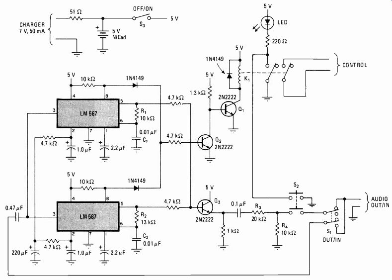
----------- Double duty. Two tones are simultaneously recorded onto
a cassette tape when switch 52 is pressed. The LM567 tone decoders, which
generate the tones, also decode them from the tape and trigger Q2 to
energize relay K,, which in turn advances a slide projector.
Current mirror linearizes remote-controlled timer
by George Hughes and S. A. Hawley Eye Research Institute, Boston, Mass.
Although setting the pulse duration of timers of the 555 variety by remote means is most conveniently done with a single control such as a potentiometer, often there is an undesired nonlinear relationship between wiper-arm set ting and output width because of the simple methods employed to achieve control. Adding a current mirror and feedback loop to the basic circuit solves the problem of linearity with little additional complexity or cost.
In general, any current passing through the pot's wiper should be minimized and the pot placed as close as possible to the circuit's interfacing operational amplifier, especially in remote-control applications, where the effects of stray coupling from various processing circuits can be considerable. A typical configuration is shown in (a). In this type of circuit, however, difficulties arise because the op amp's output voltage supplies charging currents to the one-shot's timing capacitor through a fixed resistor. As a result, the pulse capacitor width will be inversely proportional to the current driving CT and will not be a linear function of the wiper-arm position.
Adding the current mirror and the feedback loop to the circuit, as shown in (b), overcomes this drawback.
Here, the mirror's charging current is made a constant whose magnitude is proportional to only the voltage at the amp's noninverting input, V,, and hence to the potentiometer's setting. In the feedback loop, the average value of the timer's output is compared with a voltage that represents the wiper-arm position, where current injected into timing capacitor CT is such that the difference is kept small by the virtual-ground properties of the op amp. The average value of the timer's output is itself a linear representation of pulse duration, so that overall linear control is maintained.
This circuit will function with any TTL timer. Parts values are not critical and can be varied to suit a wide range of triggering rates and pulse durations. Substitution of matched dual transistors or packaged current mirrors is recommended to improve the circuit's temperature stability.
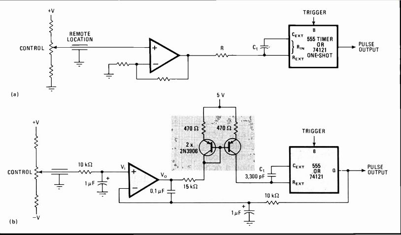
------ Current correspondence. A typical single-control pot arrangement
for setting the on-time of a one-shot (a) has a nonlinear relationship
of duration to wiper position because the current-driving capacitor,
CT, is proportional to V,(R + R1N). Adding a current mirror and feedback
loop to the circuit (b) linearizes the relationship by generating a constant
current set by V,. The values shown are for 8 <T0,,, <50 As.
Low-cost controller stabilizes heater-type cryostats
by S. K. Paghdar, K. J. Menon, R. Nagarajan, and J. Srivastava, Tata Institute of Fundamental Research, Bombay, India
Controllers for maintaining small objects at a low temperature use either complicated gas-flow techniques, that regulate gas pressure or costly commercial units that are built for general applications and must be modified to suit a particular need. Finger-type cryostats, in contrast, which control a heater on the principle of error-sensing and feedback techniques, are extremely simple, easy to implement, and inexpensive. As for stability, this circuit holds the temperature to ± 0.2 'IC over 24 hours (short-term variation is ± 0.01 K) in the range of 80 to 200 K.
As shown in the figure, the circuit may be built around an 0C23 or other power transistor, that has a fairly linear base-current-to-collector-current characteristic, eliminating the need for the additional amplification usual in circuits of this type. Error signals from a Wheatstone bridge are applied to the 741 operational amplifier act as the temperature control. The signal is then amplified by transistor Q1 and passes to Q2, which drives a resistive load and associated container that, placed inside the liquid-nitrogen-filled cryostat, heats the environment.
Thermal changes are sensed by a copper resistance thermometer, also located inside the cryostat. This element, placed in one arm of the Wheatstone bridge, reflects changes in the equilibrium temperature between the container and environment and in effect acts to cancel the original error signal applied to the op amp.
This part of the circuit serves only to correct tempera ture variations and does not set the temperature of the cryostat. Potentiometer R1 fulfills this task by setting the bias current at the output without affecting the base-driving circuit of the power transistor.
To calibrate the system, switch S1 is placed in the manual position and R1 adjusted to obtain the desired cryostat temperature. Next, the Wheatstone bridge should be balanced by adjusting the standard resistor, whose value will be determined by the center value of the circuit's copper resistance thermometer.
The gain of the amplifier stage, R3/R2, should be matched to the response of the cryostat. A nominal value might be 1,200, as in this circuit.
The system can handle heater currents of up to 850 milliamperes. Above this value, however, the current gain of the power transistor begins to fall, so that the circuit will not function effectively in the specified temperature range.
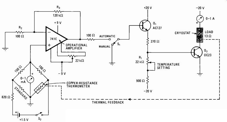
---- Cold copper. A thermal-feedback controller using a copper resistance
thermometer in a Wheatstone bridge simplifies temperature stabilization
in heater-type cryostats. This circuit holds temperatures to within ±0.2
K over 24 hours over the range of 80 to 220 K.
Noise-immunized annunciator sounds change-of-state alarm
by K. Soma Singapore Electronic & Engineering Ltd., Sembawang, Singapore
To determine the status of a multi-channeled telemetry receiver, relays are usually employed to activate lamps or light-emitting diodes set in the face of a remotely sited operator panel. However, if the call annunciator must sound an alarm each time a change occurs in the receiver's state, it often becomes vulnerable to noise pickup from external sources and produces false alarms. This circuit immunizes the receiver panel against the effects of that noise.
The simplest way to sense a change in status would be to link 39 capacitors at points P1 through P39 in the figure and to connect their common output to the gate of a thyristor at point J. Indeed, this method is often used.
But although the circuit will work, it is extremely susceptible to noise pickup from such sources as an electrical drill because all 39 capacitors form a series-parallel network that filters out most of the 12-volt pulse switchover signal when a lamp changes from green to red or vice versa. Thus, only about 100 millivolts of the original pulse is picked up at point J to trigger the thyristor.
A better method is to use transistor switches, as shown, for capacitor-to-thyristor storage and isolation to ensure that a sizable spike-not just a minor glitch from an external noise source-will trigger the alarm. A standard versatile transistor such as the 2N3904 may be used as a switch.
The standby current contributed by each transistor is less than 3.5 microamperes, and the peak current during switch-on is as much as 1 milliampere, which is sufficient to drive most current-gated thyristors- for example, the C103YY.
Note that each lamp in the display panel is effectively monitored by a transistor. Each capacitor is wired so that at least one transistor is momentarily energized only if there is a change in the lamp display input. The capacitors should have a fairly high value, which in this case is specified at 10 microfarads.
Because the currents that flow are momentary, the alarm can be canceled by pressing the spring-loaded push button. As for the system's performance, no false alarms were generated even when it was installed in a factory.
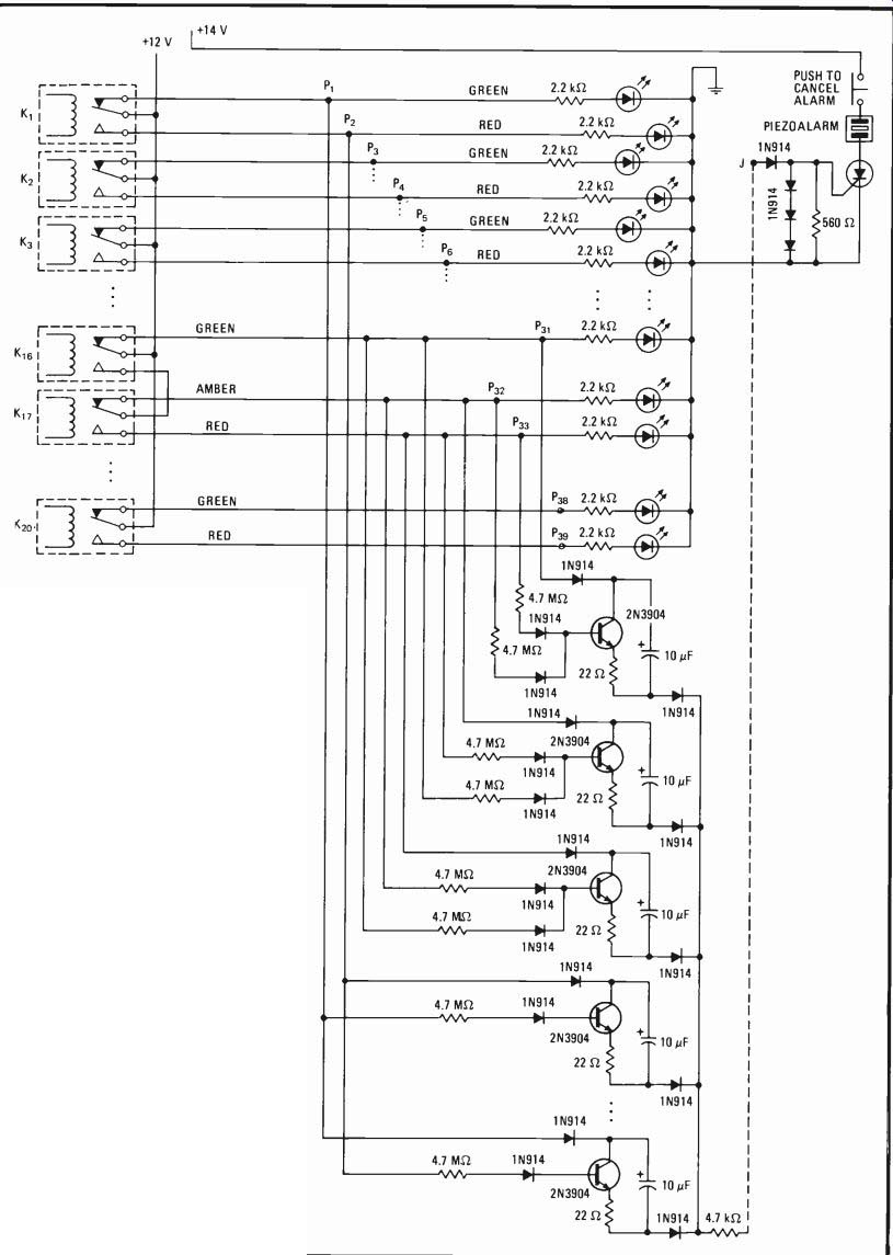
--- Noise margin. Transistor switches in a 20-channel telemetry receiver
replace a simple capacitively coupled annunciator, ensuring that external-noise
spikes do not generate false alarms in a remotely sited display panel
when there is a change in the status quo at the receiver. Transistors
ensure delivery of no less than a 6-V spike to a thyristor alarm, well
above the 100 mV from electrical noise that would normally trigger it.
MOS FETs sequence power to sensitive op amps
by J. E. Buchanan Westinghouse Electric Corp., Baltimore, Md.
Though hardly mentioned, even in application notes, operational amplifiers with double-diffused input devices often require-like many other integrated circuits powered by bipolar supplies-the simultaneous or sequential application of positive and negative voltage. This is to prevent device degradation or burnout due to forward biasing of various input-circuit diodes and transistors.
One simple and' low-cost means to meet these requirements can be achieved by using mos field-effect transistors, which have high input impedance and low output impedance, to apply power to one terminal of the op amp after sensing the presence of power at the opposite terminal. Such an arrangement is not only more reliable than any using double-pole relays, but uses less power and takes up less space as well.
The basic circuit shown in (a) ensures the simultaneous application of plus and minus voltage to a MC1556 op amp. The p-channel, enhancement-mode MOS FET in the positive supply line requires a negative gate voltage to turn on and the n-channel unit in the negative supply line requires a positive gate voltage to turn on. Therefore, this cross-coupled configuration does not allow the application of positive voltage unless a negative voltage is present, and vice versa. If one supply fails, power applied from the other supply is removed.
The FET5 are selected such that the threshold, or turn-on, voltage is roughly equal to the difference between the positive and negative supply rails. Thus both supplies must be near their rated values before either FET can turn on.
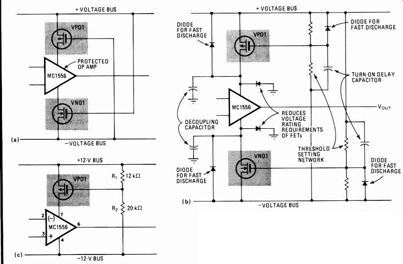
----- Millizap. Two MOS FETs protect sensitive op amps against input-circuit
damage (a) by ensuring simultaneous application of bipolar supply voltages.
Practical circuit configuration (b) includes various capacitors and diodes
for controlling turn-on delay and for transient protection. Only one
MOS FET is required for applications where the plus and minus voltages
are to be supplied in sequence (c).
In actual operation, the gates of the FETs will have to be biased via resistive voltage dividers in order to match their individual threshold requirements, and other sup porting circuitry is needed as well, as shown in (b). The addition of a capacitor at the divider will allow the turn-on time to be selected. The capacitor can also be used to compensate for a relatively slower FET in one leg or for differences in supply turn-on times.
The delay in applying the voltages to the op amp is determined by the RC time constant formed by the equivalent resistance of the divider and the turn-on delay. The decoupling capacitor is also useful for noise suppression and in supplying peak (transient) load currents. A diode may be required across the mos switch, as shown, to ensure the rapid discharge of the switched nodes when the system's supplies are turned off.
A basic circuit that will apply bipolar voltages in sequence is shown in (c). This circuit ensures that the positive supply is not turned on unless the negative supply is established. A similar arrangement is used for positive-supply predominance, except that an n-channel device is placed in the negative-supply lead.
Use of the Supertex VPO1 p-channel MOS FET (and the n-channel VN01) is ideal for all applications. They have a specified on-resistance of about 10 ohms, which is low enough to ensure that there is little voltage drop across them when they are on; in this case, the drop is only 50 my for a supply current of 0.5 mA, and it will not increase greatly despite rather heavy current flow.
Again, voltage divider R1-R2 is selected so that the VP01 will be fully on with minimum operational supply levels. Circuitry as seen in (b) is also needed.
Audio-visual controller synchronizes museum display
by William S. Wagner Northern Kentucky Unversity, Highland Heights, Ky.
A synchronized sound-and-transparency show that may be placed in any convenient area of a museum or science building can be created with this interface. Built entirely with off-the-shelf components, the cost of the circuit is below $20.
The interface controls a cassette player and a display having several illuminated panels. Each panel contains a color transparency and a source of light (in this case, a light bulb). The circuit causes these transparencies to light in sequence, while advancing the cassette tape, which contains a recorded message for each panel. Pairs of recorded audio tones control panel sequencing and thus synchronize the audio-visual display.
When the show ends, a second pair of audio tone's shuts the entire display off. Because a continuous tape loop is used, the show may be restarted by pressing a start button. A pause button is included to extend the viewing period of any panel.
As for circuit operation, when the start button is pressed, the 4043 reset-set flip-flop sets, turning on the 2N2222 transistor and pulling in the double-pole, double-throw relay. Its normally open contact closes, turning on the cassette player's motor. At the same time, the relay's normally closed contact opens, allowing the audio signal to reach the LM324 amplifier. A 667- and a 1,200-hertz tone combine to form the initial sound heard and to activate their respective 567 phase-locked loops.

---- Show and tell. This interface synchronizes sound with illuminated
panels and can be used in museum or science building displays. Cassette
tapes hold recorded segments corresponding to information seen on illuminated
display panels. When the circuit detects a chord preceding a given segment
of text, the following panel is illuminated. Also, the interface has
an automatic shut-down feature.
This causes pin 3 of the first 4001 NOR gate to go high and advance the 4017 ring counter.
When pin 2 of the counter goes high, the 2N3904 and 2N3906 transistors turn on and the triac fires, causing the first light bulb to illuminate the first transparency.
Then the recorded message corresponding to that transparency is played. At the end of the message a second pair of recorded tones (667 and 1,200 Hz) causes the 4017 counter to advance to pin 4, turning off the first light and turning on the second with its appropriate interfacing transistors and triac.
This process is repeated until all transparencies have been displayed and described. At the end of the show, recorded tones at 850 and 1,200 Hz activate their respective PLLs and the 4017 is reset so that all lights are turned off. The 4043 R-S flip-flop is also reset and turns off the 2N2222, which deactivates the relay and turns off the cassette player.
[source: ISBN 0-07-606808-0 Copyright© 1982 by McGraw-Hill, Inc. ]