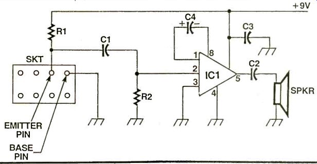
HIGH FREQUENCY TRANSISTOR CHECKER
For experimenters into building single transistor VHF FM transmitter circuits, this circuit idea could save you wasting hours of time trying to debug an apparently dead circuit. Common general purpose NPN transistors are often specified as being suitable for FM transmitters in the 88 to 108 MHz region. Sometimes these transistors can be purchased in bulk with perhaps no identifying part number. Through trial and error it has been found that not all of these 'unmarked' devices will oscillate at around 100 MHZ.
The circuit shown below checks transistors for noise emission, since it has been empirically found that devices which are good noise emitters also make good VHF oscillators. Devices which emit no noise at all, have been found not to oscillate at all. Although transistors can be DC checked, this might not be good enough to verify their `oscillatory' capability.
IC1 is an LM386 audio power amp, configured in a very basic mode, since it is only intended to amplify short term duration noise. There is no need, therefore, to waste time building a high quality audio amp. The speaker is a small 8 ohm unit. An 8 pin DIL IC socket is used to allow transistors to be quickly and easily checked. Resistor (R1) biases the transistor under test (reverse) with capacitor (C1) coupling the noise signal out to the input pin #2 of the LM386. R2 is the signal load. Capacitor (C2) AC couples the output to the speaker. C3 is required for the LM386 to operate correctly. C4 boosts the IC's gain.
To use, plug a transistor into the test socket, taking care that the emitter and base are connected as shown. Use only NPN devices. Good transistors will generate a noise output, rejects are silent!
PARTS LIST FOR THE HIGH FREQUENCY TRANSISTOR CHECKER
IC1 LM386 audio power amp
R1-1M resistor
C1-0.01 uF capacitor
R2-100K resistor
C2-10uF capacitor
C3-100uF capacitor
C4 10u F capacitor
Spkr-8 ohm mini-speaker
Sk-t-8 pin DIL IC socket
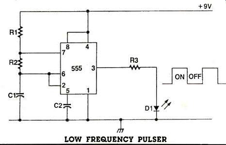
LOW FREQUENCY PULSER
For the newcomer to digital electronics, a slow pulse train source, is a very useful circuit to build. The slow speed will allow you to easily watch the high to low transitions taking place. The 555 timer is shown in the astable mode. Approximately similar "on" and "off" periods are obtained with the values given. Duration in either the "on" or "off" state is a few seconds. The output LED (D1), fed through current limiter (R3), turns on when the output goes high. Timing components (R1, R2, & C1) control the pulse frequency and "on" to "off" periods. C3 is a standard required capacitor for correct operation of the 555.
PARTS LIST FOR THE LOW FREQUENCY PULSER
IC1-555 timer R1 10K resistor R2-100K resistor R3-1 K resistor Cl-22MFD capacitor C2-0.01 MFD capacitor D1 LED, (any type)
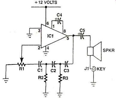
CODE PRACTICE OSCILLATOR
Here is a simple code practice oscillator you can build. It consists of an amplifier and a three stage RC feed back phase shift network R1, C1, R2, C2 and R3, C3 designed to produce an 180 degree phase shift at 655 Hz. This network couples the output of the amplifier to the inverting input of the amplifier integrated circuit. The gain of the amplifier is greater than the approximately 29 required for oscillation. Capacitor C4 increases the gain of IC1 from 20 to 200 which is greater than the required 29 to produce oscillation.
The frequency may be changed by solving the relationship f = 1/(15.3 R C). The values computed are for one of the three stages of the network and apply to the other two stages as well. The output is coupled to a small speaker in series with the code key. Capacitor C5 adjusts the volume to a listening level less than the 400 milliwatts possible.
Adjust R1 for oscillation and good tone and keying characteristics. All of the components are available from Radio Shack.
PARTS LIST FOR THE CODE PRACTICE OSCILLATOR
IC1-Audio amplifier LM 386
R1-10K potentiometer
R2, R3-10K resistors
C1, C2, C3-0.01 microfarad capacitors
C4-4.7 microfarad capacitor
C5-3.3 microfarad capacitor
J1--Phone jack SPKR-8 ohm speaker
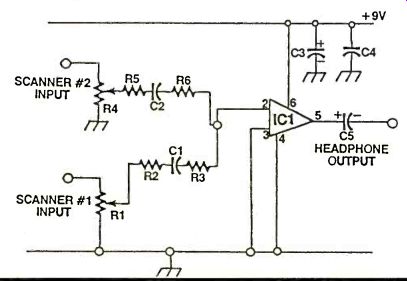
TWIN SCANNER MONITOR
Dedicated scanner radio enthusiasts are more likely to own more than one scanner (unlike the casual scanner listener). Late night monitoring through headphones limits you to one scanner only. Here's a neat circuit for monitoring, quietly and privately, through headphones, two scanners or a scanner and ham band radio. We use as the main integrated circuit, the LM 386 audio power amp. Since there is a ton of audio power available from the source scanners, the gain for the IC is set to x20 only. Two separate volume controls give you much more versatility. Current drawn in minimal (less than 10 mA) from a 9 volt battery.
IC1, is the audio power amplifier IC, driving a pair of headphones. The input from scanner #1 goes to volume control R1. Buffer components, R2, C1, R3 coming off the wiper terminal feed into Pin #2 of IC1. The second scanner #2, feed, comes from potentiometer R4. Similar buffer components, R5, C2, R6 feed the signal also to pin #2. Capacitors C3 and C4 are needed across the supply line for the IC. Finally, capacitor, C5 ac couples the output to headphones. There's plenty of drive for regular 8 ohm or 32 ohm headphones.
Set both volume controls, R1 & R4, say 1/2 way up, and then adjust both scanner volumes to give about the same sound output. Now, both channels can be individually controlled, without having to go back to the scanners every time.
PARTS LIST FOR THE TWIN SCANNER MONITOR
Resistors are 5% 1/4 w and electrolytics are 25V rating
IC1LM 386 audio IC R1-100K potentiometer R2-100K resistor R3 100K resistor R4 100K potentiometer R5-100K resistor R6-100K resistor Cl-0.1 uF ceramic disc capacitor C2-0.1 uF ceramic disc capacitor C3-100uF electrolytic capacitor C4-0.1 uF ceramic disc capacitor C5-100uF electrolytic capacitor.
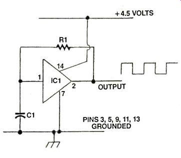
SYMMETRICAL SCHMITT OSCILLATOR
To get a pretty good approximation to a 50% duty cycle square wave oscillator, the Hex Schmitt Invertor will take some beating. Apart from the IC itself, there are only two other components! Even the ever popular 555 timer needs more than 2 components to do a similar task. The frequency is controlled by the component values for the resistor, R1 and the capacitor, C1 and the frequency set by f=1/CR (approximately). When you change the frequency, by varying either R or C, the duty cycle remains constant. This is a real advantage over the 555 which irritatingly (in spite of all its good points), changes its duty cycle as the frequency changes. Duty cycle is the ratio of either the 'on' or 'off' period to the total period.
The supply voltage has to be kept to +4.5 volts. If you're using a stock 9 volt battery, then a simple potential divider will produce 4.5 volts (e.g. two 10K resistors across the supply line). There are 6 identical devices in this IC and all unused inputs must be grounded to keep the operation reliable. Leave the output pins as is. The device used here is the SN74HC14 and the pinouts refer to this IC. There are other hex Schmitt types, but check for pin compatibility and supply requirements before using an alternative. For the components values given, R1 =10K and C1 = 0.01 uF, the frequency is 10K with a duty cycle close to 50%.
PARTS LIST FOR THE SYMMETRICAL SCHMITT OSCILLATOR
IC1-SN74HC14 hex Schmitt invertor
R1 10K resistor
C1=0.01 uF capacitor
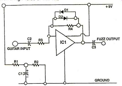
GUITAR FUZZ EFFECT
If you're a guitar player and electronics hobbyist at the same time, chances are you've most likely built a guitar amplifier, using something like the ever popular LM 386 audio power integrated circuit. To add some gusto to the basic sound, fuzz or distortion can be very easily achieved. Commercial guitar amplifiers always have a fuzz option, as guitar players consider this effect a `must'. The Rolling Stones `Satisfaction', is often named as one of the best examples of the first use of fuzz in the swinging mini-skirted 60's. The fuzz circuit produces heavy distortion by boosting the input signal by a huge amount. Typically a gain of 1000 will be sufficient to generate the desired distortion.
IC1 is a regular ac op-amp pre-amplifier, running off a single 9v battery, with a split resistor bias supply. R1 and R2 are equal in value, hence provide the Vcc/2 bias. Capacitor C1, decouples the ac signal path to ground. Regular coupling capacitors C2 and C3, appear at the input and output. Gain, for this non-inverting mode amplifier, is given by the ratio of R4/R3. R4 is the feedback resistor and is given a high value of 1 M. The input resistor has a low value, 1K, in order to produce a very high gain of 1000. Normally, of course if a clean sound was needed, the gain would be nowhere as high as this-more like around 10. The excessive gain of 1000 causes the signal to clip heavily. The balance of the fuzz effect is produced by the shunt silicon diodes, D1 and D2. These go across the feedback resistor, with opposite polarities and cause the output signal to clip at 0.6 volts in each direction.
PARTS LIST FOR THE GUITAR FUZZ EFFECT
LM 741, op-amp
R1--100K resistor
R2--100K resistor
R3--1K resistor
R4--1M resistor
C1-100uF electrolytic
C2--0.47uF ceramic disc capacitor
C3--0.47 ceramic disc capacitor
D1--1N4148 silicon diode
D2--1N4148 silicon diode
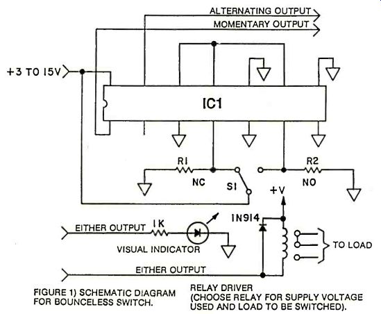
SIMPLE SWITCH DEBOUNCER
By C. R. Fischer
While the speed of digital electronics makes it possible to do things that the relatively slow human being can't touch, sometimes this quickness can be a problem. For example, if we were to hook up an everyday pushbutton to the clock input of a counting circuit, we would find that the counter would jump through random numbers rather than counting one step at a time as we would want.
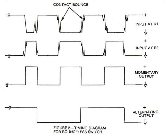
The problem is not with our counter, but is actually within the switch itself. Whenever the switch is opened or closed, the contacts may make and break several times before coming to rest. This phenomenon is known as contact bounce, and it causes problems when digital circuitry interprets each bounce as a separate switch closure.
One simple and inexpensive solution is shown in figure 1. To eliminate any bounce, we use a SPDT momentary switch to set or reset a flip-flop. Since the state of the flip-flop is set by the positive edge of the signal, any other noise is ignored. When the switch is depressed, the flip-flop is set high, and when the switch is released, the output goes low again (See Fig. 2). Since the chip is a dual flip-flop, we can use the other half for a second switch, or for an alternating output by wiring it as shown. The top half is connected as a binary divider, which goes high and low on subsequent clock pulses. This allows us to use a momentary pushbutton as a regular on/off switch, with a minimum of hardware. By using the IC to drive a relay or SCR, we can control loads much greater than the small amount of current we would put though a small pushbutton.
This is a very simple circuit, and it can be powered from DC supplies of 3 to 15 VDC. If the chip is not being used to drive an active part like an LED, it can be powered from batteries with very low power consumption. This would make the circuit attractive for remote controls and similar applications, Finally, note that the IC is a CD 4013, and is a CMOS device. For this reason, be sure to use a socket and avoid handling the IC until the circuit is finished. For now, give it a try and see how many uses you can find for it!
PARTS LIST
IC1--CD 4013 Dual D Flip-Flop
S1--SPDT momentary switch
R1, 2--100k 1/4W resistors
Misc.-14 pin socket or Molex Soldercons, breadboard or perfboard, hookup wire, Etc.
Also see: All About Robots
adapted from: Electronics Handbook Vol. X