By Conrad Persson
---------
Information, photos and illustrations on which this article was based were provided by B & K Precision.
The introduction of integrated circuits a few years ago created a revolution in electronics. The immediate result was a reduction in the size of electronic products, an increase in their speed of operation and reduction of power consumption. That revolution has continued at breakneck speed since then, with the result of an array of products that couldn't even have been dreamed of before: laptop computers, Walkman-type stereo equipment, compact disc audio and laserdisc video, electronic watches, credit card calculators. The list could go on and on.
Besides the obvious effects on size and performance on every type of electronics equipment, the introduction of ICs had a number of other effects on the electronics world. Standard logic ICs, such as the 74 series, allowed circuit de signers to begin designing by using functions rather than voltage/current relationships. For example, a circuit designer who wanted to include AND gate into a design didn't have to study how they worked and design them. He simply could go out and buy a 7408 quad 2 -input AND gate and - as long as his circuit provided the gate with the proper source voltages and logic inputs-it would work.
The effect of ICs on servicing
The effects of ICs didn't stop at the design engineer and consumer levels. ICs also had a profound effect on servicing technicians. For instance, technicians often enhance their understanding of a circuit by tracing the circuit visually, taking voltage readings at strategic points in the circuit and following the logic of the design. Trying to do that in a circuit containing ICs can be an exercise in frustration. You can trace the circuit up to the IC's pins but if you want to know what's going on inside, you have to obtain the literature of the ...
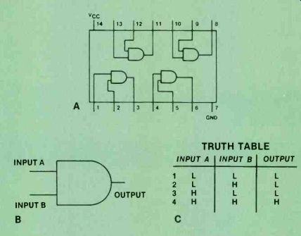
Figure 1. Quad 2 -Input AND gate, 7408, is simply an IC that contains, on
a single chip, four AND gates, each with two inputs.
... manufacturer and study it. And as often as not the circuitry will be shown as functions rather than actual electronic components.
This has introduced additional mystery into a subject that is already surrounded by mystery, making it increasingly difficult to comprehend.
Then comes the question of testing ICs, especially logic ICs.
Because with logic ICs you're frequently dealing with data that's flowing at high rates, you can't just probe with the usual test equipment: DMM, oscilloscope and so forth. Some specialized equipment is needed: logic probes, logic pulsers, IC testers.
Testing ICs
You can proceed to test ICs in a number of ways. For starters there is the old standby, the DMM.
It will reveal a lot of things about ICs. Of course, there are also a lot of things it will not reveal. For example, with power to the board un der test turned off if you suspect a specific IC, you can probe its pins with the meter set to the OHMS scale. This approach will reveal certain classes of problems like opens or shorts. With power applied to the device under test, the meter can be switched to DC VOLTS and used to probe do levels.
An oscilloscope likewise can be used to diagnose certain types of faults in IC circuits.
For most effective trouble shooting of logic ICs, though, you need to use test equipment specifically made for the purpose. The specific types of IC test equipment you'll need will depend on the amount and complexity of the digital equipment you'll be servicing.
Here's a list of some of the IC test equipment that's readily available from test equipment manufacturers and distributors you're familiar with:
- Logic probe
- Logic pulser
- Logic test clip
- Logic timing analyzer
- Logic state analyzer
- IC tester
Logic ICs
Before proceeding with the theory and operation of the test equipment, let's take a look at some of the circuitry it's designed to test. Figure 1 is a logic representation of a quad 1 -input AND gate. The standard semiconductor industry designation for one of these ICs is 7408. For those of you unfamiliar with the concept of design and operation of these devices, here's a review.
As you know, computers and computer -based equipment use a lot of logic gates. In the early days of integrated circuits, before an entire computer could be fabricated on a single IC chip, semiconductor manufacturers recognized that if they fabricated several gates on a single IC chip, computer designers could design their circuits based on these ICs. Given the state of the art of IC fabrication at the time, multiples of gates in a chip made sense.
A quad 2-input AND gate, then, is simply one IC package that contains four AND gates, each of which has two inputs.
Figure 1B shows a single AND gate. Its truth table is shown in Figure 1C. If no input signal is present at input A or B, there is no output. If there is an input signal present at either input A or input B, but not at both, again there is no output. Only if there is an input signal present at both A AND B is there an output. That's why it's called an AND gate.
With the right test equipment it's a piece of cake to test one of these devices during trouble shooting. First check to see that VDD and Vss are present. If not, there's a problem somewhere, but not necessarily in this IC. If those two supply voltages are present, it remains to check the operation of each of the four individual gates.
Note that one gate has as inputs Pins 1 and 2, and its output is Pin 3. Another gate has Pins 5 and 6 as inputs and Pin 4 as output. The third gate has Pins 8 and 9 as in puts and Pin 10 as output, and the fourth gate has Pins 12 and 13 as inputs and Pin 11 as output. To test this IC, once you have checked for the presence of the correct sup ply voltages, you simply need to check each gate to see if its characteristics correspond to its truth table. We'll discuss that in detail when we get into the IC testers portion of this article, but basically, it's just a matter of monitoring the output of each gate one at a time while you apply, first, no signal at both inputs, then a signal at each output alternately, then a signal at both inputs. If you get an output signal when there is a signal present at both inputs, but not signal otherwise, the gate is operating properly.
The OR gate Logically enough, the 74 series of ICs also includes a quad 1 -input OR gate, 7432 (see Figure 2). Not surprisingly, the source voltages are at the same pins as on the 7408, Pins 7 and 14. In addition, inputs and outputs to each of the gates are at the same pins.
Testing the 7432 proceeds in a similar manner to testing the 7408. First, verify that the correct source voltages are present at Pins 7 and 14. Assuming that these signals are present, you can proceed to testing the individual gates. No signal at either input to any of the gates will result in no signal at the output of that gate if the gate is operating properly. A signal at either input or at both in puts to either gate should result in an output.
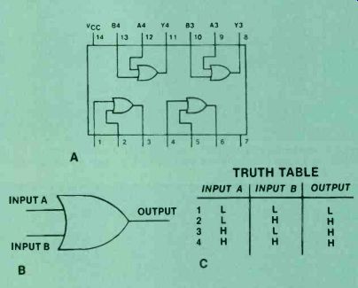
Figure 2. Quad 2 -Input OR gate, 7432, contains four OR gates, each with
two inputs.
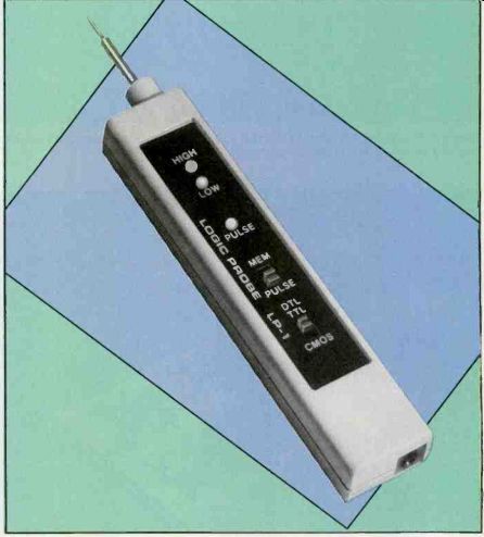
Figure 3. A logic probe can be used to determine if a given logic IC pin
is at a HIGH logic level, a LOW logic level, or if it is pulsing.
The logic probe
The logic probe, Figure 3, indicates the logic state of point being tested, whether it is at a logic HIGH or LOW. A sophisticated probe will have indicators to show if the test point is HIGH or LOW or exhibiting pulses. Some will even have a memory or pulse stretcher that will show the presence of a 1 -shot pulse that is of duration so short that either it's in sufficient even to light the indicator, or lights it too briefly to be recorded by the human eye.
The indicators used on these logic probes to show the logic state of the pin being tested are usually LEDs. In some cases a single LED is used to indicate any of the conditions: HIGH, LOW or pulsing, while in other cases, individual LEDs are used for each indication.
Let's say you're doing troubleshooting using a sophisticated logic probe that is capable of testing a number of different kinds of logic circuits: TTL, DTL, CMOS. You would connect the probe's power input to the power supply from which the circuitry being tested derives its power. Connecting the probe in this manner will indicate the approximate value of signal voltage that constitutes a logic LOW or HIGH. For example, the power supply voltage for a CMOS logic circuit is 18V. A logic LOW in this circuit would be about 30% of that value or 5.4V.
A logic HIGH in this circuit would be about 70% of 18V or approximately 12.6V.
If you suspect a specific IC, it would make sense once you have the logic probe connected into the circuit's power supply to go directly to that IC. Otherwise, use the time-tested method of starting approximately in the middle of the circuit, and let the results at that point guide you upstream or down stream a half -circuit at a time.
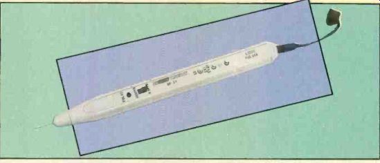
Figure 4. A logic pulser may be used to infect pulses, or trains of pulses,
at inputs to logic ICs. Used in conjunction with a logic probe, it can help
pinpoint problems.
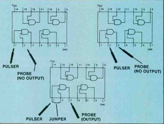
Figure 5. By pulsing and probing the appropriate inputs and outputs of a
logic IC, you can determine if it is operating properly or if it's defective.
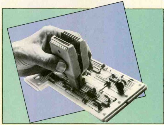
Figure 6. A logic monitor clips over the leads of an IC to be tested. LEDs
read out the logic level of all pins simultaneously.
The logic pulser
The logic pulser, Figure 4, is the active counterpart to the logic probe. When its tip is placed against an IC pin and you push the button, it will inject a pulse, or a train of pulses, into the IC.
Here's how you might test a 7408 quad 2 -input AND gate, using a pulser and probe (Refer to Figure 5). Starting with one of the gates, say the one with input Pins 1 and 2 and output Pin 3, connect the probe to Pin 3 for the duration of the test. Then apply a pulse, using the pulser at Pin 1. There should, of course, be no output.
Then apply a pulse at Pin 2. Again, there should be no output. Then, observing precautions to avoid circuit damage, place a jumper across Pins 1 and 2 and apply a pulse to both pins simultaneously. If the gate is working properly, a pulse should appear at Pin 3 and be ob served on the logic probe.
To make sure that the complete IC package is good, place the logic probe at Pins 4, 10 and 11 in turn and pulse input Pins 5 and 6, 8 and 9, and 12 and 13, just as you did Pins 1 and 2 to check each of the other gates.
By applying logic properly, or simply by following the circuit's truth table, you can use the logic pulser and probe in combination to test any other similar logic IC.
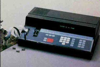
Figure 7. If you plan to troubleshoot a lot of digital logic circuitry, you
might want to use an IC tester.
Logic monitors
Another inexpensive test device for logic ICs is the logic monitor, Figure 6. This a unit that clips right over the IC to be tested. The monitor features an LED for each of the pins on the IC that reads out at any time what the logic level is at that pin.
IC testers
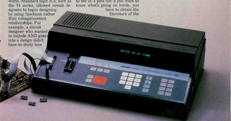
If you don't test a lot of digital ICs, the logic probe and pulser and possibly the logic monitor will probably be all the logic test equipment you'll ever need. If, however, you plan to troubleshoot a lot of digital logic circuitry, you might want to have available an IC tester (See Figure 7), one that you can connect to an IC and receive an immediate display of that IC's condition. With one of these units, you don't have to pulse or probe, and you don't have to interpret the condition of one or more LEDs. You simply set the device up for the IC to be tested, plug the IC into the tester's socket and test it.
Conventional IC testers test chips by generating test patterns that exercise all possible input -state combinations of the chip being tested. For example, the NAND gate shown in Figure 8A has a maximum of four input -state combinations. These four possible input combinations yield four test patterns that the tester must carry out to completely test this device. When the four test patterns and the resulting output of the device for each of the test patterns and the resulting output of the device for each of the test patterns (1) through (4) (Figure 8B) are arranged in a table, a truth table is developed.
As noted by the name, the truth table represents response that should be obtained for test patterns (1) through (4).
IC testers produce each of the test patterns (1) through (4), apply one pattern at a time to the inputs; and check the output result for each test pattern. The correct results for a given chip are known and are held in memory. The tester checks the results obtained from the chip under test by executing each test pattern, and then decides if the results match the predetermined correct results. If all of the results agree, the chip is declared good. If any of the results do not match with the predetermined correct results, the tester declares the chip defective.
Figure 9 shows the truth tables and comparisons between a good device (chip No. 1) and a defective device (chip No. 2). Note how a chip No. 2 test pattern (4) does not match the predetermined result.
The tester notices the error and declares the chip as defective.
Limitations to conventional testing Conventional functional tests are perfectly suited for all out -of -circuit device tests. In out -of -circuit testing conditions, the tester is free to toggle each input of the chip HIGH or LOW, thereby executing all patterns of the chip's truth table.
For many in-circuit applications, inputs to the chip are wired in ways that prevent the tester from executing the predetermined test pattern that corresponds to the chip's truth table. Called hard wiring, this is commonly used.
Figure 10A shows again a 2 -input NAND gate with its inputs free from imposed states. In this case, the expected customary truth table can be executed and, as expected, the gate output exactly matches the response required by the tester (designated "TESTER REQUIRES" in all truth tables shown).
Figure 10B shows the same 2 -input NAND gate wired with in put A tied to Vcc (+5V). This is a very common in -circuit configuration. Assume that the gate is functional. Now we'll attempt conventional functional testing of the gate. Notice what has happened to the test patterns. During the execution of test patterns (1) and (2), input A of the chip was prevented from going to the LOW (0V) state.
Most important, notice what happened during test pattern (2): The tester tried to pull input A low.
However, input A is tied to+ 5V.
During test pattern (2) this condition prevented the expected test pattern from being executed.
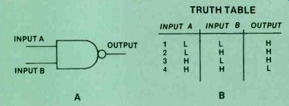
Figure 8. An IC tester applies a pattern of signals to the input pins of
a logic IC and tests for the response. If the response is different from that
expected, the IC is declared to be defective.
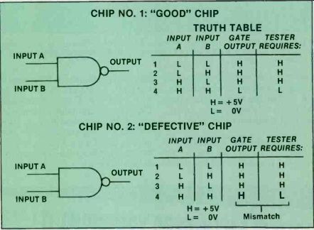
Figure 9. The input/response pattern of chip No. 1 is the pattern expected,
so chip No. 1 is labeled "good." The pattern for chip No. 2 does
not match the expected pat tern, so it is branded "defective." Therefore,
in this case the expected output was not produced.
Instead of the chip outputting a HIGH during this test pattern, the chip outputted a LOW, causing the tester to declare the chip "defective" even though it is good.
Figure 10C shows the same 2-Input NAND gate wired as an inverter; both leads are tied together. This is another very common configuration that will be encountered during in -circuit testing. Again assume that the gate was previously checked and is known to be good. Here's what happens if you attempt conventional functional testing of the gate. Again, notice what has happened to the test patterns. During test pattern (2), input A is expected to go HIGH; but the jumper connecting the two inputs together make opposite states on each input impossible. During test pat tern (3), the opposite input state orientation occurs; but again the jumper connecting the two inputs makes this impossible. During test patterns (2) and (3), an invalid result is outputted from the gate.
The tester will certainly give a "defective" result during test pat - tern (2) or (3), or both. Again, due to the unexpected nonstandard in put wiring, the tester will declare the chip as "defective" even though the chip is known to be good.
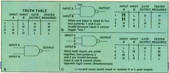
Figure 10. The Truth Table for the NAND gate in A, which has its inputs from
imposed states, is the correct Truth Table. In B, Input A is tied to Vcc.
and in B the inputs are hard -wired together. A NAND gate in either of these
configurations will test "defective" on a conventional tester. When
both inputs are wired together, test patterns 2 and 3 are invalid because
Input A and B cannot attain opposite logic states simultaneously. When input
is one wired to Vcc test patterns 1 and 2 are invalid because Input A cannot
toggle "low." I =Invalid state; could result in random H or L gate
output.

Figure 11. An IC tester with COMPARE mode can store the Truth Table input/output
patterns of a hard-wired IC and use this "new" pattern as a criterion
for testing similarly wired ICs. Rejecting test patterns 1 and 2 ,compare
Testing only considers...
valid patterns 3 and 4 ...
These patterns yield the "new" Truth Table. The "new" patterns 1 and 2 will be used by the Model 560 Compare Mode to test additional "Figure 7" circuits.
IC testers that can learn
Some IC testers are able to circumvent the problem of nonstandard configurations by including a learning or storage mode. Using this mode, the IC tester exercises the input of a gate that is known to be operating properly in a non standard configuration with the normal set of input signals, but in stead of declaring the nonstandard output to signify a defective IC, it accepts the output to be proper for that configuration and stores it.
Take, for example, the con figuration we've discussed before shown in Figure 11. Because one of the inputs of the NAND gate is tied back to Vcc, the response of this circuit will not be that of a standard NAND gate. When the IC tester is placed in the compare mode, now the obtained gate output represents the "new" function of the NAND gate as wired in this example. This new gate output (response) develops a new truth table for the NAND gate. The new truth table, shown beside the circuit of Figure 11, becomes the criterion against which other circuits wired in the same way will be tested.
Testing ICs, the same only different
Troubleshooting methods for electronic circuits have changed considerably since the advent of ICs, yet the object of the exercise is the same: stimulate a circuit segment with a known signal and observe the response. If the response is different from what was expected, you strongly suspect that the defect lies there and test some more.
The broad range of IC test equipment sophistication allows the servicing technician to choose between spending more time with relatively simple, inexpensive test devices, or to save time with more sophisticated, but more expensive, test equipment.
It's important also to keep in mind that because of the huge numbers of different kinds of ICs being manufactured, no programmed tester could possibly test them all. So even if it makes sense to own one of the sophisticated testers, it still will be necessary to maintain skills with logic pulsers, probes and similar testers to test the logic ICs that haven't been programmed into the high-dollar testers.
Also see:Test your electronics knowledge