By John A. Ross -- Ross is a technical writer and a microcomputer consultant for Fort Hays State University. Hays, KS.
Editor's note: Previous articles in this series discussed the evolution of memory devices that led to the configurations currently found in memory cards, as well as the "adjacent" circuitry found on the Zenith memory card -- circuitry that provides multiplexing and timing signals. Part VI describes the operation of the computer's memory circuits and some troubleshooting steps you can take when the unit is not working properly.
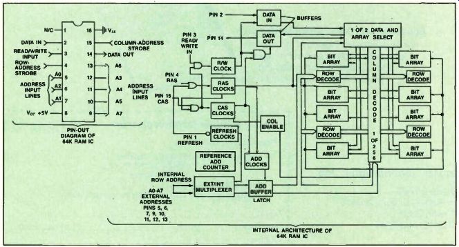
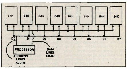
The Zenith memory card contains five banks of memory ICs. Depending on how much memory the owner purchases, each bank contains either nine integrated circuits or nine sockets that allow the addition of more ICs. Figure 1 shows the pill-out connections of the memory IC and a block diagram of the internal structure of the IC. Figure 2 shows a block representation of the eight data information storage ICs connected without the extra parity IC. The first eight ICs in the bank work sequentially as the actual storage devices; the last chip serves as a parity storage device.
When dealing with the operation of the memory circuitry, keep in mind that you will find the same types of signals at the individual pins of each IC in the working bank. Figure 3 shows a sample bank of memory and a byte of information that might typically be stored in it. In this example, the typical Zenith numbering system will show that ICs U412 through U419 serve as the addresses and that U411 serves as a parity storage.
U419 gives the least significant bit and U412 supplies the most significant bit for the 8-bit information byte. Any ac cess to the sample bank will cause each chip to contribute either a logic 1 or a logic 0 to the byte.

Figure 1. The Zenith memory card contains five banks of memory ICs Each bank
contains either nine ICs or nine sockets that allow the addition of more ICs.
Figure 1A shows the pin-out connections of the memory IC. Figure 1B shows
a block diagram of the internal structure of the IC.
Address signals
The row-address and column-address signals start the processes that select the proper row and column for forming a byte. During the actual address, the row address signal initially causes each multiplexer in the circuit to choose between a logic 1 and a logic 0. This selection places either group of bits on the multiplex bus. Not surprisingly, this operation fulfills the definition of multiplexing -- the process of alternately putting different signals on the same bus lines.
Through the multiplexing of the row- and column-address signals, the memory device can first latch onto the eight most significant bits and then onto the eight least significant address bits from the input/output address bus. This seemingly simple operation sets up the row and column selection.
To see how this comes into play, we could consider a 64K memory IC as one large 256-by-256 matrix. Remember that each data RAM chip has 256 rows and 256 columns of bits. Multiplying 256 by 256 yields 65,536. One K in the jargon of logic is actually 1,024, not 1,000. Dividing 65,536 by 1,024 yields 64. Thus, a RAM chip that contains a 256-by-256 matrix is a 64K chip. This 64K memory IC stores more than 65,000 single-bit words; the 256K chip (a 512-by-512 matrix) stores almost 280,000 single-bit words.
Row-address strobe, multiplex-timing and row-address signals work together to gate the least significant bits onto the multiplex address bus. Before the signals are applied to a bank, the program address logic (PAL) IC, U455, deter mines the correct bank for an address.
The PAL also acts as a traffic controller for any data information that flows between the address and data-buses of the system and the memory circuitry. By latching onto these bits, the selected bank chooses one of the 256 rows.
After the row selection, the column selection begins. Here, column-address strobe timing, column-address strobe and row-address signals team up to latch the most significant bits onto the multiplex bus. The selected bank latches those bits off the bus and uses them to choose one of the 256 columns of the bit matrix. When the gating occurs and the bits from the selected rows and columns of the eight ICs in the bank combine, the data-information byte forms.
If you look at the RAM IC illustrated in Figure 1, the function of each signal and how it affects the operation of the RAM becomes readily apparent. Once again, the example of one IC represents the functions of eight RAM ICs in the bank. After the address decoder IC uses the I/O address bits to decide which row-address strobe line to enable, the column-address strobe signal arrives.
Decoding the address bits that arrive at pins 4 through 7 of the memory ICs determines the logic needed for the bank selection. A normal read or write condition will cause the row-address strobe signal found at pin 4 of only the memory ICs in the selected bank to go to a digital active low state. Multiplexed ad dress bytes are applied to pins 5, 7, 12, 11, 10, 13, 9 and 1 of the 256K memory devices. In a computer that uses 64K ICs, no multiplexed signal is needed at pin 1. 256K chips will have a signal at pin 1.
As the user of the microcomputer types information on the keyboard, the information becomes data written into the memory banks. The RAMSEL (RAM-select) signal logic must appear as a digital active low for any data transfer to take place. If the RAMSEL signal reaches an active high, the tri-state data buffer, U470, will go to an off state.
An inactive tri-state buffer will block the flow of data from either direction. A digital active low state at pin 3 of the memory devices, the write-enable signal, allows the memory bank to accept written data. In this case, the tri-state buffer gates data from the I/O bus to the system RAM. A digital high state at pin 3 sends the bank into the opposite read state. During the read condition, the tri state buffer gates the information data from the system RAM to the I/O bus.
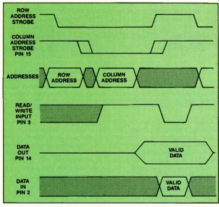
Figure 4 shows the waveforms displayed during the read-write/read-modify-write cycle.

Figure 2. This block representation shows the eight data information storage
ICs connected without the extra parity IC. The first eight ICs in the bank
work sequentially as the storage devices: the last chip serves as a parity
storage device.

Figure 3. This is a sample bank of memory and a byte of information that
might be stored in it. The typical Zenith numbering system will show that
ICs U412 through U419 serve as the addresses and that U411 serves as a parity
storage. U419 gives the least significant bit and U412 supplies the most significant
bit for the 8-bit information byte. Any access to the sample bank will cause
each chip to contribute either a logic 1 or a logic 0 to the byte.
Illustrated at pin 4 of the ICs, a logic zero row-address strobe signal causes the selected bank to latch onto the eight least significant bits found on the multiplex bus. Seen as a logic 0 at pin 15 of the random-access devices, the column-address signal tells the bank that the RAS* has selected to latch onto the eight most significant bits. Data information to and from the RAM banks feeds out through the data-in and data out lines found at pins 2 and 14.
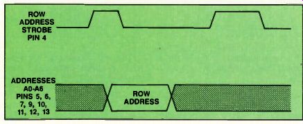
In the October issue, we discussed the refresh cycle for the banks of the system memory. A refresh cycle occurs when an address in the system memory goes into the read state. When speaking of the normal read and write operations, we recognized that only the signal at the selected bank changed. During the refresh cycle, all memory banks are selected. As a result of the interrupt re fresh request or IRQO signals, the RASO through RAS4 signal found at pin 4 of every chip in all the banks goes to a digital active low state. Figure 5 depicts the waveforms seen during the refresh cycle.
Parity In our discussion of memory chip activity, we have only looked at the actual RAM storage and transfer operations.
Several other necessary operations remain. To study those operations, we need to go back to the ninth chip in the bank, the parity storage device. however, let's define parity first. A parity bit does not change the meaning of the computer word. The use of parity essentially gives the microprocessor a simple error-detection device used during memory circuit operation. An odd parity error check detects problems with the 9-bit word consisting of the MDO through MD7 bits plus the parity bit MD8 at pin 14 of the data storage ICs.
Figure 6 gives a pictorial representation of parity-bit generation and checking. Each byte of data information re quires eight bits plus the ninth parity bit.
A parity bit does not change the meaning of the computer word. The use of parity essentially gives the microprocessor a simple error-detection device used during memory circuit operation.
As the microprocessor writes new in formation to the memory, the parity circuit determines the parity of the eight bits and stores that bit in the ninth location. When the processor begins the read sequence for the byte, the parity circuitry again determines the parity and compares it to the already stored parity bit. In any microcomputer system, the chance exists that one bit may change its logic state during the transfer to and from a memory location. If the "beginning and after" parity bits differ, the parity circuit sends an interrupt to the microprocessor. With the interrupt, error messages appear on the monitor display.

Figure 4. These waveforms are displayed during the read-write/read-modify-write
cycle.

Figure 5. These waveforms are seen during the refresh cycle.
Zenith, like most of the microcomputer manufacturers, employs odd parity as a checking method. Odd parity produces a binary word that has an odd number of ones by adding a one to the data information that has an even number of ones. When a technician uses an oscilloscope or a logic analyzer to check the operation of the memory circuit, naturally he looks for some type of change. When odd parity is used to check the quality of the binary word, a change in signal occurs. If the byte contains all zeros, the signal would resemble a line frozen at zero. Odd parity ensures that at least one bit of the word will exist as a one. Unfortunately, the parity bit, whether odd or even, only detects an odd number of errors. Any detection of errors involving the 2, 4, 6 or 8 bits of the word will require more sophisticated diagnostic tools.
Although the circuitry involved with parity generation and error detection seems similar to other circuitry already discussed, some fundamental differences also appear. Most notably, the parity-storage IC, the same type of circuit as the data-storage IC, has pins 2 and 14 electrically separated. In the data-storage memory IC, these pins tie together. Pin 2 provides the entry tie point for the parity bits; pin 14 provides the exit tie point for the parity bits. The data word through the memory data bus is applied sequentially to pins 8, 9, 10, 11, 12, 13, 1 and 2 of the parity genera tor, U451. A digital logic 1 signal appears at pin 4 of the parity generator as the data RAM outputs go to an inactive state and pin 14 of the parity RAM goes to +5V. Here, the parity checking be gins. If an even number of ones appear in the data information byte, a logic 0 or even signal shows at pin 5 of U451.
Figure 7 shows an example of a data word that contains an even number of ones along with the addition of the parity bit. U457, a NAND gate, sees the logic 0 at its pin 4 and inverts the signal to its pin 6. From there, the logic 1 goes to pin 2, the data output, of the all-parity RAMs. If the data string contains an odd number of ones, the opposite digital signals show at the respective pins of U451 and U457. As the selected memory address location stores the 8-bit data word, it also stores the generated parity bit, which guarantees an odd number of one.
If some condition, such as a power supply-induced noise spike or an imperfect data-bit, occurs, U451 senses the mismatch and places a logic 1 signal at pin 5. Remember, the circuitry compares the stored parity bit from the write operation with a recalculated value generated during the read operation.
Figure 6 supplies a block diagram of the parity comparison check. This logic 1 causes the NAND gate to reset a dual flip-flop. U464, a hex inverter, inverts the digital active-high output of the flip flop and applies the signal to the I/O channel check line as an active-low parity error.

Figure 6. In this representation of parity-bit generation and checking during
read/write cycles, each byte of data information requires eight bits plus
the ninth parity bit.
Troubleshooting parity errors
If repeated parity errors occur, the parity circuitry provides an easy-to troubleshoot test point. Not surprisingly, the mention of parity-error detection brings us to circuit diagnosis. When parity errors repeatedly occur, check the data random-access system memory for any possible errors. Connect a logic analyzer to all bits. Then you can manually calculate the correct value of the databit from the data information present and compare the value of the correct parity bit against the value of the generated parity bit. If this step suggests that there are problems in the parity generation and error-detection circuitry, you can then disable that circuitry with I and 0 debugging commands. Working from the Monitor ROM internal test program, a technician uses the 0 debugging value to output a value to the location of 100 hex or the parity disable port. A one will disable the parity check circuitry, a two will disable the parity generation circuitry, and a three will disable both areas. With the use of the debugging command, you can cause a parity read condition to occur, because this command causes the input of data from the port.
The first thing to do is make sure none of the components in the data storage circuitry are defective. Diagnostic software routines can help by writing data to the RAMs, then reading this stored data back out and comparing the read data with the original written data.
A number of diagnostic routines are available. For starters, a built-in set of checks test the memory card. If these initialization tests find an error, they generate an interrupt, a display that gives the defective IC designation (such as U449) and the hexadecimal address.
If repeated RAM errors appear, you can use the unique set of monitor ROM based tests that Zenith supplies. You can access these tests by simultaneously pressing the Ctrl, Alt and Insert keys.
At the prompt, which appears after pressing these keys, type "test," then choose the option for checking the system memory. This test sequence will exercise the system memory, although it is slow.
If the test sequence uncovers a suspected IC, a hexadecimal address will appear at the display. As with the checking of the parity circuitry, you can use debugging commands, such as E for entering a hexadecimal address and F for filling the hexadecimal address at the monitor ROM level. Using these debugging commands, you can force the RAM circuitry to operate as it would if normal operating conditions existed.
With an oscilloscope or a logic analyzer, you can monitor activity at a suspected bank or IC. As the test routine progresses through its checks of the memory circuits, the monitor may display a suspect hexadecimal-based address such as 00E1:20E1. You can convert this hexadecimal code back to its original binary form to find the location of a possible defective memory IC. Each portion of the code helps indicate the location of the address error. The left-hand set represents the segment number; the right-hand set represents the offset. The segment portion of the error message identifies the bank that failed. The off set shows the defective internal address of the defective chip.
If you use the write/read address 00E1 20E1 as an example, a hexadecimal-to binary conversion follows this format:
0/0000 0/0000 E/1110 1/0001 2/0010 0/0000 E/1110 1/0001
Converting the write portion of the error message changes hexadecimal 00E1 to the binary 0000 0000 11100001. Converting the read portion of the error message changes the hexadecimal 20E1 to the binary 0010 0000 1110 0001. The codes given by the write/read operation don't match and show that an error condition exists. The four zeros to the right of the colon indicate a boundary failure.
The technician should check for possible configuration problems. Studying the other four digits of the hexadecimal code, the technician should note where the first digit falls. If the first digit falls between zero and three, the defective IC lies on the first bank. If the first digit has a value higher than three, the defective IC is in the second bank of RAM chips. After concluding which bank contains the possible defective IC, a technician can use the remainder of the code to find the IC slot location. By converting the remainder of the hexadecimal code to binary and then simply counting from the designated zero RAM location, a technician can find and replace the defective IC.

Figure 7. During parity checking, if an even number of ones appear in the
data information byte, a logic 0 or even signal shows at pin 5 of U451. This
figure shows an example of a data word that contains an even number of ones.
-----------
Problem areas in memory-address logic circuitry
Problem:
Wrong bank selection.
Solution:
Replace U455, the program-address logic IC.
Problem:
Repeated error indication at the same memory address
Solution:
Replace U465, U473 and U474 multiplexers.
Problem: A column-address strobe-gate logic error causes wrong addresses.
location.
high-order
Solution:
Replace U467 (OR gate), U468 (dual flip-flop) and U469 (tri- state buffer). Problem:
Data dropout affects system memory.
Solution:
Replace the U470 tri-state data latch.
Figure 8. The repeated display of the same memory address location generally will point to some area of the memory-address logic circuitry. These are the probable suspect areas in that circuitry.
-------------
Commercially available diagnostic test routines also can help service technicians. Available in either 3 1/2-inch or 5 1/4-inch floppy-disk formats, the diagnostic disks contain tests for each section of the microcomputer. The diagnostic test disks are one of the most valuable tools for the technician. Procedures performed in the other simple test routines, such as the monitor ROM and debug routines, work automatically. Considering the memory section, the diagnostic test routines check the parity-generation and error-trapping circuitry and the data RAM circuitry. Each check of the RAMs fills the IC banks so that an operating condition occurs and then initiates the read and write cycles. Systematically running each bank through a series of tests completely exercises each IC and helps to expose the suspect chip.
After isolating the problem to a defective memory IC location, you can substitute a known-good RAM IC for the suspect IC. If you don't have a memory device in stock, you can switch the suspected IC with any good IC in the random-access banks. (Remember to use the proper anti-static precautions. Semiconductor memory devices have a high sensitivity to static.) If the microcomputer again stalls during start up and the same memory address appears on the screen, you know it wasn't the RAM chip, so you can look else where. The repeated display of the same memory address location generally will point to some area of the memory ad dress logic circuitry. Figure 8 lists probable suspect areas in that circuitry.
The memory circuits constitute one of the more complex sections of the microcomputer. Because of technological advances, the look and feel of the memory section has begun to change.
With the advent of new IC technology.
DRAMs have increased in capacity and have diminished in size. Microcomputers with a memory capacity of 4Mbytes have become more common Today, many microcomputers feature single in-line memory modules (SIMMs). Instead of featuring an entire memory card, the microcomputer chassis features each bank of non-removable ICs on a small removable card that plugs into a motherboard. The same criteria that apply to the older style RAMs apply to the newer memory devices.
In Part VII, we will take a look at the video section of the microcomputer, and we will again see a use for the memory circuits.