AMAZON multi-meters discounts AMAZON oscilloscope discounts
LEARNING OBJECTIVES:
Upon studying this section on surface mount technology, the student should be able to:
1. Determine land sizes and footprints for many surface-mounted components and devices.
2. Properly identify the side of a pc board on which surface-mounted and conventional through-hole components can be placed when both technologies are used on a common board.
3. Select, test, and properly apply solder paste to surface-mounted components.
4. Select, test, and properly apply adhesives to surface-mounted components.
5. Be familiar with the wide variety of soldering methods used in surface mount technology.
6. Hand solder surface-mounted components.
7. De-solder surface-mounted components.
0. INTRODUCTION
Surface mounting stems from the technologies of flatpack cases, shown in Sec. 14 Fig. 27, and hybrids where surface-mounted devices are soldered inside a ceramic or plastic package having through-hole leads. For these, it appears that the conventional methods of design and manufacturing have, to a large extent, reached the limit regarding factors of cost, reliability, size, and weight. With the emergence of surface-mounted technology (SMT), the generation of lighter, smaller, and more dense pc boards at lower costs and higher reliability has been realized.
Surface-mounted technology involves the bonding of components and devices directly to the surface of the board and connected directly to the conductor pattern, thus eliminating the requirement of drilling holes in the board.
The sizes of surface-mounted components (SMC) and devices (SMD) are very much smaller than their equivalents made for conventional through-hole installation. Because SMT is relatively new, all equivalencies are not available. In addition, there is a great deal of nonuniformity of standardization among manufacturers of SMT components and device packages. As a result, both conventional and SMT are required to be used on most pc board designs. With the improvement in the technology, more and more board area will be devoted exclusively to surface mounting.
1. CONDUCTOR PATTERN LAYOUT
Recall that in Section 11, the layout of terminal pads for components and devices, together with their orientations, was easily obtained with the use of drafting templates. Unfortunately, surface-mounted conductor pat tern layout does not lend itself to the relative ease of layout experienced with conventional through-hole design. This is largely due to the lack of standardization of SMT package designs and the wide variation in component tolerances in the industry. In addition, land pattern design is process-dependent, which means that the same design can experience different manufacturing defects de pending on the process variables. (Land pattern is the term used in SMT to define the terminal pads to which the device leads are soldered). This is brought about by the fact that each manufacturer has to establish specific land pattern designs that will function with their materials and processes. For this reason the land patterns presented in this section and the techniques for their design serve only as guidelines.
Common land patterns, also referred to as footprints, to be discussed include: ceramic rectangular resistors and capacitors (small outline RC and CC); tantalum capacitors (small outline molded plastic and welded-stub); tubular passive components (metal electrode leadless face or MELFs); transistor chip patterns (small outline transistors or SOTs); small outline integrated circuits (SOICs); small outline J lead devices (SOJ memory and SRAM packages); and chip carriers (plastic leaded chip carrier or PLCC, and leadless ceramic chip carrier or LCCC).
The land pattern design parameters for ceramic rectangular resistors and capacitors are shown in FIG. 1. The dimensions of component length (L), width (W) and height (H) and the termination length of the metal bands (MB) are measured first. To determine the width of the land (A) and its length (B), the following relationships are used:

---FIG.—1 Land pattern design parameters for resistors and capacitors.
For capacitors:
For resistors:

--- TABLE 1 Resistor and Capacitor Land Pattern Dimensions Component/
Dimensions are in decimals of an inch. ---
Resistors are much thinner than capacitors and require a longer land to prevent misalignment due to their lower mass. The space between the lands (G) is the same for both components and is determined as follows:
G =L —2MB —0.02inch
The overall length of the footprint would thus be G + 2B. Two examples of land patterns for ceramic resistors and capacitors are shown in TABLE 1.
The procedure to determine the land patterns required for molded plastic and welded-stub tantalum capacitors is similar to that for ceramic resistors and capacitors, as shown in FIG. 2. Once the dimensional information is obtained for each component type, the following are used to determine the footprint dimensions and spacings:
For molded plastic:
Amp = w + 0.010inch
Bmp = h + MT
G = 1 — 2MT — 0.020 inch W + 0.010 inch
For welded stub:
A= H + MT
G =L—2MT—0.020 inch
Two examples of tantalum capacitor footprints are shown in TABLE 2.
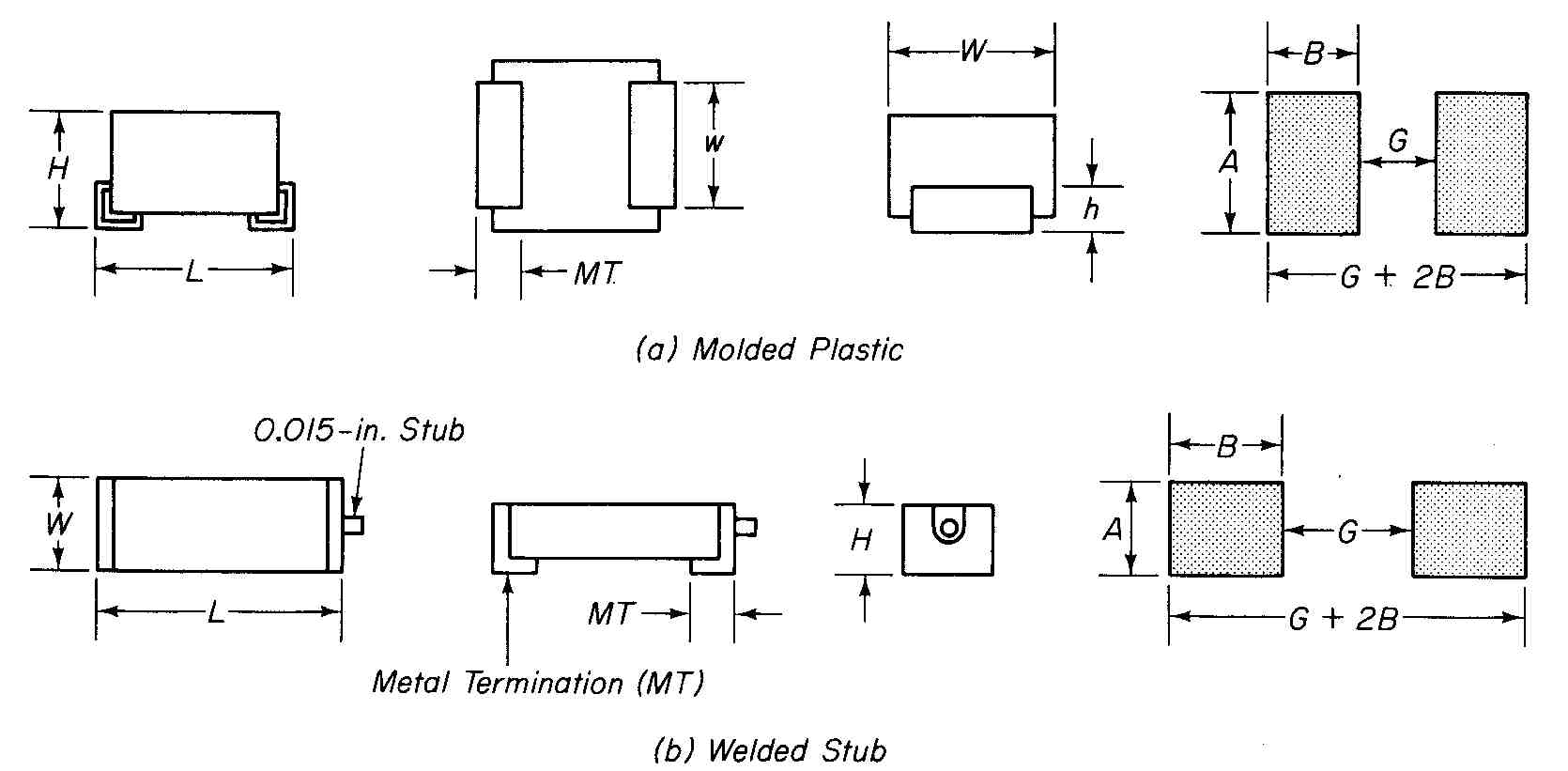
FIG.—2 Land pattern design parameters for tantalum capacitors: (a) molded
plastic; (b) welded stub.

--- FIG.—3 Land pattern design parameters for MELFs.
Surface-mounted tubular passive components (MELFS) are resistors, ceramic and tantalum capacitors, and diodes. These packages have metal end caps that are soldered to the lands. Because these packages are round and there is a tendency for them to roll out of position, a slot must be provided in the lands if they are to be soldered using the vapor reflow method. If the component is to be wave soldered, an adhesive is used which eliminates the need for the slots.
The measurements used for the design of MELF patterns are shown in FIG. 3. The following are used to determine the footprints for this package style:
AMELF = diameter (D) + 0.010 inch
BMELF = diameter (D) + MC
G = L—2MCM—0.020 inch
If a notch is required, notch depth =B/2 and notch width = 0.010 inch. An example of MELF land pattern dimensions is given in TABLE 3.
Some of the most commonly used small outline transistor (SOT) chip pat terns are the S0T23, S0T89, and the S0T143 packages. These footprints are shown in FIG. 4. When designing the land patterns for SOTs, the distance between land centers is generally made equal to the on-center dimensions of the device leads. At the same time, the land should be made 0.015 inch longer than the lead on each of its ends. Many footprints are available from graphic suppliers, such as Bishop Graphics, that will accommodate a variety of designs.
The criteria for selecting commercially available footprints for small out line integrated circuits (SOICs), or R-packs, are much less complicated than for those designs discussed previously. The land width and length should be 0.030 inch and 0.075 inch, respectively. The on-center spacing of the lands is typically 0.050 inch. This will result in about a 0.015-inch space between adjacent lands. To determine the space (S) between rows of lands, the relationship S = body width—0.01 inch is used.

---TABLE 3 Sample of MELF Land Pattern Dimensions
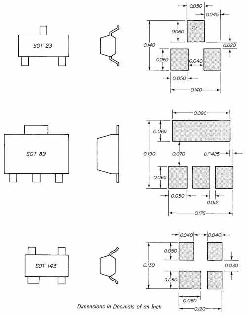
---FIG.—4 Small outline transistor patterns.
The footprint of a SOIC, together with typical dimensions of various other packages with different lead counts, is shown in TABLE 4. The footprint design for plastic leaded chip carriers (PLCCs) and leadless ceramic chip carriers (LCCCs) is shown in FIG. 5. Note that the PLCC chip has leads that turn under the package. This formation is referred to as J leads as opposed to those typical of SOT packages, which are called gull wings. The footprint is determined by the following:
on — center lead spacing = 0.050 inch
land width = 0.025 inch
land length = 0.075 inch
dimension A and B = X + 0.030 inch (for PLCC)
dimension A and B = X + 0.0 70 inch (for LCCC)
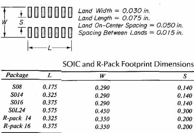
---TABLE 4 SOIC and R-Pack Footprint Dimensions
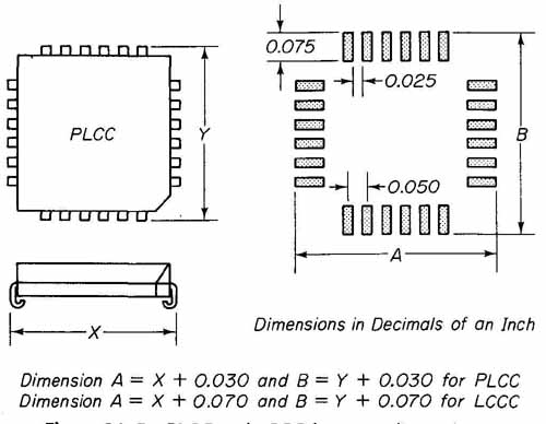
---FIG.—5 PLCC and LCCC footprint dimensions.
Note that for square chip carriers, dimension A = dimension B. This is not true of rectangular packages. These dimensions for a variety of square and rectangular chip carrier footprints are given in TABLE 5.
Surface-mounted components are soldered to the pc board by either vapor phase, solder wave, or infrared processes that are discussed in Sec. 5. Variations in land pattern dimensions may be required for the same component for a different soldering process. One of the common problems encountered is the varied degree of solderability at termination ends. This can cause misalignment of components with fingerprints. Also, components such as resistors and capacitors, instead of remaining flat, may end up in a standing position, called tombstoning. If these components are positioned too close to each other, a large component may shadow a smaller one causing insufficient solder or solder bridges to result. For these reasons, it is essential that all land pattern designs first be evaluated through the processing of test boards.
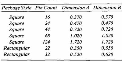
---TABLE 5 Overall Dimensions of PLCC and LCCC Land Patterns
Package Style | Pin Count | Dimension A | Dimension B
Some recommended spacing considerations for SO, SOJ, R-packs, and PLCC packages are shown in FIG. 6. These spacings also take into account automatic assembly and testing requirements.
The following societies may be consulted for additional design information: The Institute of Interconnecting and Packaging Electronic Circuits (IPC), Electronics Industries Association (EIA), and the Society of Manufacturing Engineers (SME).
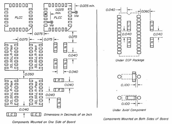
--- FIG.—6 Minimum land-to-land or land-to-pad clearances: (a) components
mounted on one side of board; (b) components mounted on both sides of
board.
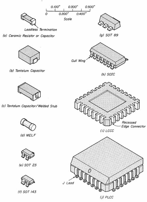
---Fig. 7 Surface mount component and device packages: (a) ceramic
resistor or capacitor; (b) tantalum capacitor; (c) tantalum capacitor/welded
stub; (d) MELF; (e) SOT 23, (f) SOT 143; (g) SOT 89; (h) SO1C; (i) LCCC;
(j) PLCC.
2. SURFACE MOUNT ASSEMBLY
The surface mount packages discussed in the preceding section are shown in FIG. 7. Figures 7a through d show leadless resistor and capacitor pack ages with metal end caps or terminations, and FIG. 7e, f, g, and h illustrate SOT and SOIC packages with gull and modified gull wing leads. A leadless chip carrier with recessed edge conductors is shown in FIG. 7i, arid FIG. 7j is a plastic chip carrier package having J leads.
As mentioned previously, a wide variety of components are not available for surface-mounting applications, resulting in pc board designs incorporating this technology together with conventional through-hole insertion. An exception to this is in the design of memory boards, where all required packages are available for surface mount.
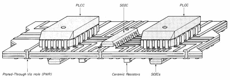
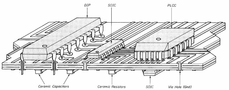
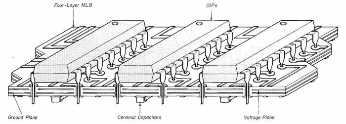
---FIG.—8 Type I, II, and iii SMT assemblies: (a) type I—exclusively
surface mounted components and devices on top or on top and bottom; (b)
Type II—insertion components on top with surface-mounted components on
one or both sides; (c) type III—insertion components on top with surface-mounted
components on the bottom.
As a result of the requirement for a combination of both technologies, SMT assemblies have been divided into three categories which describe their application. These are shown in FIG. 8. Type I assembly contains only surface-mounted components on a single-sided, double-sided, or multilayer pc board. Where components are placed on the bottom side, the tack of the solder paste applied to the lands prior to assembly is sufficient to hold them in place during board handling and baking prior to reflow soldering. If the reflow soldering is done by vapor-phase or infrared processes, the solder paste will continue to hold them in position. If wave soldering is used, all components must be held in place with an adhesive on any side that will be passed over the wave. Because many devices are heat sensitive, one side of the board may be vapor-phase re flowed while the less temperature-sensitive components on the other side of the board are wave soldered. This procedure is more common with type II and III assemblies that combine surface mount with through-hole designs. Type II assemblies place SMCs on one or both sides of the board with through-hole insertion components on the top only. Type III assembly places through-hole insertion components on the top side with SMCs on the bottom side.
Due to their size and delicate mechanical features, SMCs are mounted manually with the aid of a vacuum pipette or, for volume production, by automatic component placement. Prior to placement, solder paste and adhesive are applied as required. These processes are discussed in detail in Secs. 3 and 4, respectively. The two primary functions of automatic equipment for SMT assembly are picking up the components and placing them onto the correct lands. For this reason, this type of equipment is generally termed “pick and place.” Assembly equipment having single or multiple pick and place vacuum heads are available. Components are placed sequentially with X, Y, and Z movements of the vacuum head. Automatic machines are usually fed with components that are bulk packaged on reels or in magazines called DIP sticks, which are plastic tubes that channel parts into the machine.
When manually installing SMCs, they should be handled by their bodies, not by their terminations or leads. In addition, care should be exercised so as to avoid smearing solder paste or adhesive onto the packages that would interfere with solder joint formation and result in short circuits.
In any process of assembly used, the component terminations or leads must register squarely on lands. Even though the surface tension of the melting solder paste tends to pull misregistered components into place, this should not be counted upon. If misregistration is not detected on SMCs that have been secured with adhesive, correction is difficult and time consuming.
3. SOLDER PASTE
To solder SMCs to pc boards, solder paste or solder cream is first applied to the footprints by automatic dispensing with a syringe, screening, or stenciling, after which the components are assembled. Solder paste is the standard term, although rosin-based materials are referred to as creams. Solder paste is a homogeneous combination of minute pre-alloyed solder particles that are suspended in a flux system. The solder particles are spherical as a result of blowing or splashing melted solder onto a spinning, wheel in a controlled atmosphere. Their round shape has less tendency to clog screens as well as having minimum surface oxidation.
The flux system is made up of a flux base and a getting or suspension agent that are blended together. The formulation of this flux system is a well guarded secret in industry. The proprietary ingredients involved give the paste body, the ability to withstand soldering temperature and time without breaking down or losing efficiency (thermal resistance), chemical strength (effectiveness), and a consistency that makes it suitable for application by screening, stenciling, or syringe dispensing.
Factors that govern the selection of a solder paste for a specific application are particle size, flux activators, metal content, and rheological properties such as viscosity, tackiness, slump, and working life. Each of these factors will be described in detail.
If the screening process of flux application is to be used, the particle size should be small enough to pass through a 200-mesh (200 holes per square inch) screen. Larger particle sizes may be used if stencils or syringes are the method of application.
The flux promotes wetting action between component leads and the surface mount lands. Solder paste is available with three different types of flux: rosin flux (R), mildly activated rosin (RMA), and fully activated rosin (RA). The R flux contains no activators and may not have an aggressive enough cleaning action for acceptable solderability. The RMA fluxes are the most generally used for surface mount applications. The RA fluxes are used only when a more potent cleaner is required. They should be avoided whenever possible, however, since the characteristics of surface-mounting techniques prevent thorough flux cleaning under and around components.
The metal content of the solder paste determines the size of the solder fillets that will form about the component leads. Solder pastes have different melting temperatures. For the soldering of plastic surface-mounted packages, a lower-melting-point paste should be used compared to that used for ceramic packages. If higher shear and tensile strength are required at elevated temperatures, tin—antimony alloy solders are used. Tin-lead alloy solders are not compatible with gold-plated terminations. For this application, indium-lead alloys are recommended. Compatibility with silver-plated leads requires a tin—lead solder containing 2% silver.
The most widely used solder pastes for mounting plastic components to FR-4-type pc boards are those having either 63% tin and 37% lead (eutectic) with a melting point of 360°F (183°C) or 62% tin, 36% lead, and 2% silver, which has a melting point of 355°F (179°C).
The rheological properties of the solder paste are controlled by the gelling or thickening agents and secondary solvents. The solvent dissolves the flux and controls the tackiness of the paste as a result of its evaporation rate. The degree of tackiness is an important factor in the selection of past since it holds the SMCs in place during placement, baking, and handling before reflow soldering.
The viscosity of solder paste changes when agitated by either syringe dispensing, screening, or stenciling. This is due to the fact that these pastes are thixotropic fluids; that is, they become more fluid when worked and more viscous when allowed to rest. The recommended viscosity of solder pastes as related to their method of application is as follows:
Syringe dispensing: 300,000 to 400,000 centipoise (cP)
Screening: 450,000 to 550,000 cP
Stenciling: 550,000 to 750,000 cP
These viscosity measurements may be taken with a Brookfield viscometer using a TF spindle at 5 revolutions per minute.
The term slump refers to the ability of the paste to spread, yet stay within the bounds of footprints after it has been deposited. The degree of slump is determined mainly by the percentage of metal in the paste. Sample test boards with land patterns are used to evaluate how far the paste spreads after it is applied. This is to ensure that it does not spread onto adjacent lands before or after component assembly.
The working life of solder paste is defined as the length of time from when it is removed from the container and goes through all of the fabrication processes—its application, SMC placement, and baking—to the solder reflow process. The degree of tackiness determines if the working life of the paste has elapsed.
When pc boards with SMT components and devices are soldered by the vapor phase or the infrared reflow process, solder paste often throws small spherical particles of solder referred to as solder balls. These can measure 2 to 5 mils in diameter. Since they usually end up on the insulated surface around footprints, they are easily dislodged and create a potential short-circuit problem.
Solder balls form either as small particles that float away with the melting flux before the larger mass of paste melts or as heavily oxidized particles that cannot be removed by the flux and activators. These particles are pushed aside as the molten solder melts and flows about the connection.
To test for paste acceptability in terms of solder ball formation, several 6- to 10-mil-thick paste patterns are screened onto a suitable sample of nonmetallic material such as FR-4 pc board or ceramic—or frosted glass. The test panel is then put through a solder reflow process and the paste examined. It is accept able if no solder balls are generated and the solder deposits are large shiny spheres having smooth surfaces. Acceptable and unacceptable solder ball formations are shown in FIG. 9. Note that a few particles having diameters of 5 mils or less are acceptable. Anything larger, or a halo or clusters of particles are unacceptable. Some of the methods used to eliminate the formation of solder balls are better control of the amount of paste applied and using fresh paste with the most active flux allowable.
The application of the solder paste to the lands by any method must be checked for coverage and for registration. A number of acceptable and unacceptable configurations of paste deposits on land patterns are shown in FIG. 10. FIG..10a through d are acceptable with part (a) preferred. Those labeled as unacceptable (Fig.10e through h) would result in short circuits or unreliable solder joints. Soldering of pc boards is discussed in Sec. 5.
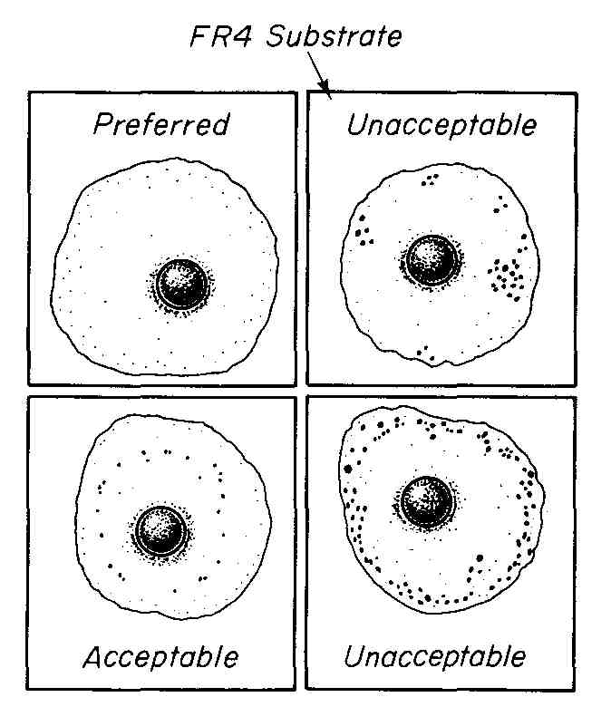
---FIG.—9 Test panel solder ball formations.
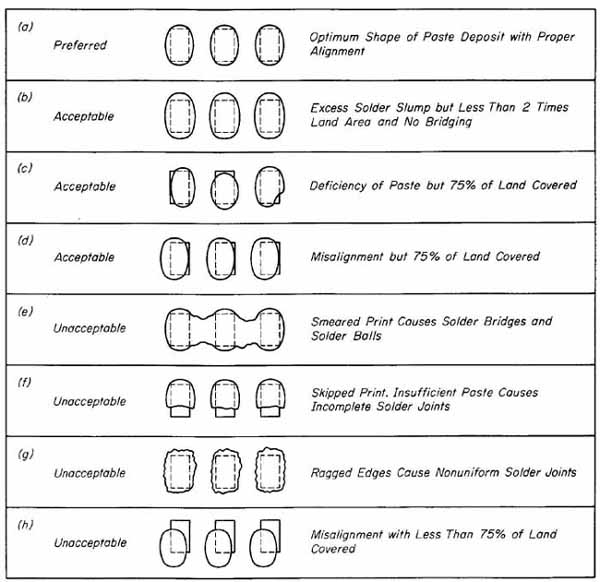
--- FIG.—10 Acceptable and unacceptable solder paste deposits.
4. ADHESIVES
The two most common types of adhesives used for SMCs are epoxies and acrylics. Unlike thermoplastic adhesives, which harden and soften with temperature cycles, these adhesives, once hardened, will not soften or lose their bond strength with elevated temperatures. Because epoxies and acrylics are classified as thermosetting adhesives, they will withstand the heat of the solder wave and will retain the components tightly to the pc board as it passes over the wave.
To be most effective, the adhesive selected must be properly applied and cured. In addition, the adhesive must have specific precure, cure and postcure properties that are compatible with SMT. The adhesive must also have sufficient green strength, which is similar to the tackiness of solder paste, to hold the component in place before curing. It should also have the proper viscosity to fill the gap between the component and the board without spreading onto the footprints.
For most applications, one-part adhesives are preferred over the two-part (mixing) type, which requires more time to prepare and has a short working life since it begins to harden when the two parts are mixed. Even though one-part adhesives have a shorter shelf life, refrigeration extends this life.
An adhesive that cures in the shortest time at lower temperatures is preferred provided that it possesses sufficient bond strength. Greater bond strength results from elevated temperatures with the same curing time. however, the temperature must not be so high as to adversely affect heat-sensitive components or deform the board.
The adhesive should have minimum shrinkage properties when cured to prevent excessive stress on component bodies. Curing time should not be accelerated since voids may occur which would decrease the effectiveness of the adhesive. If outgassing occurs during the cure process, flux may become entrapped from the solder paste, which will result in difficult cleaning problems.
The curing of adhesives is accomplished in infrared (IR) ovens for epoxies and with a combination of UV light and heat for acrylics. The thermal-cured epoxies are popular since the IR oven can also be used for reflow soldering with out requiring the expense for a UV light system. Acrylic adhesives have a faster curing time, however, and are preferred for high-volume production.
Acrylic adhesive must extend beyond the component so that the UV light will strike it and begin the chain reaction of curing. If this polymerization does not occur, heating alone will allow uncured adhesive under the component, resulting in voids and entrapped flux during the soldering process. Ultraviolet thermal systems use a 2 kilowatt lamp set at a distance of about 4 inches from the board. The adhesive is exposed for about 15 seconds, and the full cure will result in less than 2 minutes in an JR oven.
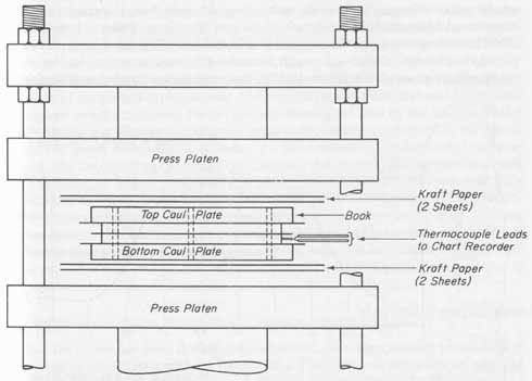
--- FIG.—11 Thermal profile of epoxy cure in an IR oven.
Epoxies have a curing time of about 5 minutes when the temperature is gradually increased to about 305°F (150°C). The board is then allowed to cool slowly to room temperature for another 10 minutes. A typical thermal profile curve of epoxy adhesive cure in an JR oven is shown in FIG. 11. (The procedure for obtaining a thermal profile is discussed in Section 15.)
After the reflow soldering process has been completed, the adhesive no longer serves a useful function. Its postcure properties are essential, however, in that it must not absorb moisture and must remain nonconductive and non-corrosive.
The application of adhesives is accomplished by three common methods: screening, pin transfer, and syringing. Syringing is generally preferred because in many instances, there are components on the board before the adhesive is to be applied. In these situations, screen and pin transfer applications cannot be used. Syringing forces the adhesive through an orifice by electric, hydraulic, or pneumatic pressure. This system, although not as fast as other methods of application, controls the rate of adhesive flow very accurately to ensure uniformity of deposit.
The pin transfer method employs a grid of pins which are dipped simultaneously into the adhesive. This array of pins is then automatically positioned and lowered to the board. The adhesive has a greater affinity for the nonmetallic substrate than for the metal pins. Gravity causes a uniform amount of adhesive to be deposited from the pins.
Screening is done using the same techniques as the silk-screen process de scribed in Section 13. The application of surface mount adhesives, however, requires a stainless steel screen and the appropriate mesh number. As in the use of any adhesive, the manufacturer’s instructions should be carefully observed.
The correct application of adhesive for large and small components is shown in FIG. 12 together with the correct dot (adhesive deposit) sizes for various land sizes. The deposit of adhesives for a large component after the application of solder paste is shown in FIG. 12a. Note that there are two adhesive dots on the substrate between the lands and a smaller dot on the bottom of the component. This will ensure that the space under the component is filled with adhesive. However, excess adhesive should be avoided since it will interfere with proper solder joint formation. Approximate adhesive dot sizes used for typical lands are shown in FIG. 12b, c, and d.
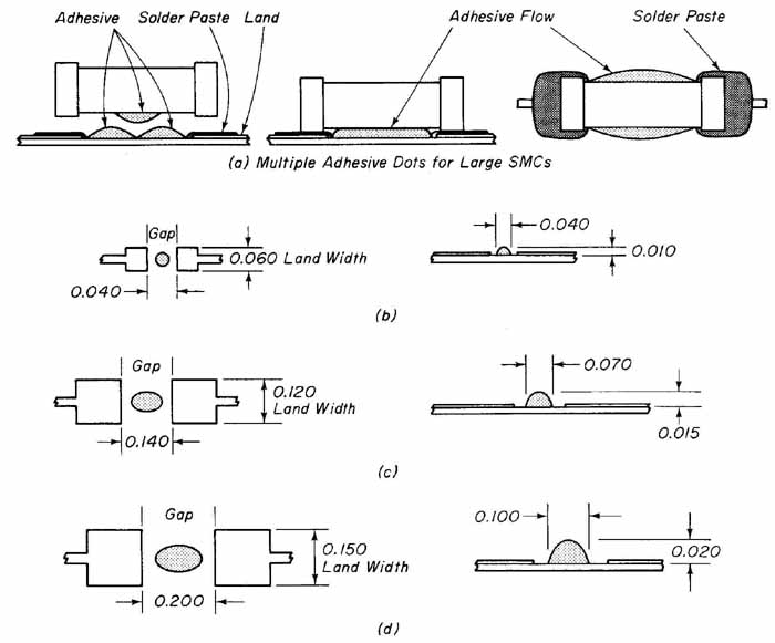
--- FIG.—12 Adhesive application for large and small components.
5. SOLDERING FOR SMT
The soldering process in SMT is termed reflow soldering. The joining of metal surf aces of the lands with the terminations of the components and devices is completed by the mass heating of the predeposited solder paste. When the paste melts, solder fillets are formed between the lands and the terminations. Automated volume production methods include wave soldering, vapor-phase soldering, and infrared reflow. Laser soldering is another automated process which is faster than hand soldering but not as fast as the other production processes. Because laser soldering is a relatively new process, it is more expensive and the technical problems involved with solder defects and component dam age have not all been resolved. For these reasons, laser soldering is confined to specialized applications and is viewed as a complement to rather than a replacement of the other soldering processes.
Wave soldering for pc boards has been discussed previously. Some modifications of the process are required for boards which incorporate both conventional and surface-mounted components and devices. These modifications require special features to accommodate higher board densities as well as components being mounted on the bottom side of the board. These features, shown in FIG. 13, are primarily air knives, and a dual solder wave.
The first air knife overcomes the problem of not being able to smooth the applied flux with a brush roller, due to the surface-mounted components on the bottom of the board. The air knife effectively removes excess flux and smooths the flux coating over lands and component terminations.
The dual soldering wave is a required feature because of the components mounted to the bottom of the board. The first wave is turbulent, which ensures sufficient distribution of solder across the board as it passes. The velocity of the solder allows it to penetrate between tightly spaced components and leads. The solder jet is pointed in the direction of the conveyer travel, which results in no solder skips. However, the applied solder is very uneven and excessive, causing bridges and icicles. The second wave is the conventional type used for through-hole components. As the board passes over this smooth wave, excess solder is removed along with any bridges and icicles.

---FIG.—13 Air knives and dual solder wave reduce solder defects of
surface mounted components.
Immediately after the board leaves the second solder wave, it passes over a hot air knife. A jet of hot air, whose temperature is above the melting temperature of solder, is directed at the soldered joints. A properly wetted solder connection will be unaffected by the jet of air since the surface tension of the solder exceeds the force of the air. Any solder that is not bonded, such as bridges, icicles, and excess amounts that were not removed by the second solder wave, is removed by the hot air knife. To prevent the blowing of solder up through holes in the board and, at the same time, remove just the right amount of solder, the air knife’s spacing from the wave, and its angle to the board, in addition to the air temperature, volume, and velocity, must be accurately controlled. The hot air process also acts as a method of quality control since the super- heated air stress-tests each solder fillet and uncovers any land or pad that is not properly soldered.
To maintain and monitor precise temperature control of each phase of the wave soldering process, a temperature profile of the board is required. This is done by placing one or more thermocouples at strategic locations on the board and recording the temperature variations as it passes through the preheat and wave soldering stages. The recommended temperature parameters for preheat rate, temperature differential between preheat and solder wave, time of the board in the wave, and cool-down rate are 2°C/second maximum, 100°C maximum, 3 to 4 seconds, and -5°C/second, respectively. The procedure for obtaining a temperature profile is discussed in Section 15. A temperature profile for a pc board as it is passed through a single solder waveis shown here .
Vapor-phase and infrared soldering processes are much different from wave soldering, where the source of solder and most of the required heat are provided by the wave. This significant difference for both processes will be de scribed in detail.
For type I assemblies vapor-phase or infrared soldering processes are used exclusively, while types II and III assemblies require the use of wave soldering as well. The source of heat for vapor phase comes from the condensation of vapors from a boiling liquid onto the metal terminations, solder paste, and lands. Since heat is also transferred by convection, the work is heated uniformly. Also, the board is protected from heat damage because its temperature cannot exceed that of the boiling point of the liquid. This automatic vapor- phase soldering system makes use of either batch or in-line equipment. These are shown in FIG. 14. In the batch system shown in FIG. 14a, the work is lowered through a secondary vapor layer, usually Freon TE, into the primary vapor, which is an inert perfluorocarbon such as FC-531 1 from the 3M Corporation. The board remains in the primary vapor zone, whose temperature is approximately 419°F (215°C), for 20 to 30 seconds. The board is then raised into the secondary vapor zone and allowed to drain off the primary fluid (30 seconds to 1 minute). The temperature of this zone is about 225°F (107°C). Because of the secondary vapor zone, the cooling coils at the top of the chamber, and the high density of both vapors, the loss of expensive perfluorocarbon is kept to a minimum. The high density also acts to reject air and moisture from entering the process.
The in-line system, shown in FIG. 14b, does not have a secondary vapor zone. The board is passed through a saturated vapor zone in 20 to 30 seconds. There are vapor condensing surfaces at the top of the chamber as well as at the input and output locations. With an optional vapor recovery system added to the machine, the vapor loss can approach that of the batch system.
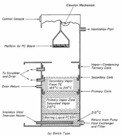
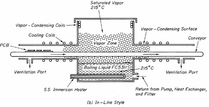
--- FIG.—14 Batch and in-line vapor-phase soldering systems: (a) batch
type; (b) in-line style.
The infrared reflow soldering process passes the boards along a conveyer between top- and bottom-mounted JR quartz iodide lamps having ceramic reflectors for higher wavelength or JR panels called area source emitters. The basic arrangement of this system is shown in FIG. 15. Both natural and forced-air convection are used on these systems. Test panels should be run through the process to ensure that the emitted wavelength is correct, so that nonuniform heating of the board will be avoided. Also, the optimum air convection needs to be determined to cure the solder paste properly and prevent the formation of solder balls or splatter. Infrared soldering is the generally preferred process because it is more controllable for higher yields and lower operating costs.
Some automated soldering systems provide a forced cooling stage as the final process in the soldering operation. This has been shown to improve the strength of solder joints.
For small soldering tasks, hand soldering is commonly employed. It is also used as a means of reworking or correcting soldering defects resulting from an automated process. The power of the soldering iron used on SMCs, such as ceramic resistors, capacitors, and diodes, should not exceed 22 watts. These components could easily be damaged if subjected to extreme heat. A pointed soldering tip is preferred and its temperature should not exceed 700°F (370°C). Excessive pressure against connections should be avoided to prevent delamination of lands. In addition, the tip should be in contact with the connection for only 1 to 3 seconds, depending on the type of component.
Because of their small size and light weight, along with the fact that they have no leads inserted through drilled holes, SMCs tend to move off of the land when hand soldering. This problem can be overcome by placing a droplet of adhesive onto the substrate between lands. Using solder that has a diameter of 0.031 inch is ideal for transferring the adhesive to the board. Any cyanoacrylate adhesive will prove effective. These adhesives are more commonly known by their trade names, such as Crazy Glue, Instant Glue, or Super Glue. It is important that the deposit of glue be accurately placed and that the amount be controlled so that it does not spread onto the lands when the component is pressed into place. This would inhibit the formation of a proper solder connection. Since this adhesive is fast acting and very strong, care must also be taken to ensure that the component is properly placed. It would be virtually impossible to move it after the adhesive has set. Once the adhesive has cured, soldering of the connection may begin. Solder having a maximum diameter of 0.031 inch is shaped to a fine point for this delicate work. The time to solder each connection should be no more than 2 to 3 seconds for chip resistors and 1 to 2 seconds for delicate IC leads.
Because of the small size of the parts and the requirement for precision craftsmanship, a magnifying lamp, such as that shown in FIG. 16, is essential. Flow charts for types I, II, and III assembly and processes are shown in FIG. 17.
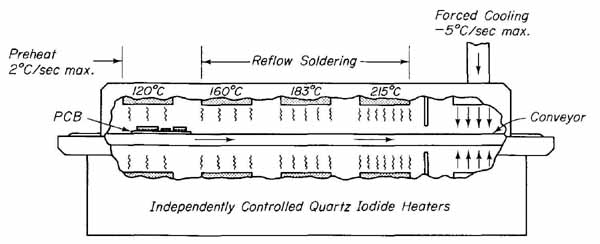
---FIG. —15 In-line infrared reflow soldering system with forced cooling.
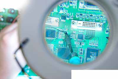
--- FIG.—16 Soldering and rework of small surface mount technology devices
is best accomplished under a magnifying glass.
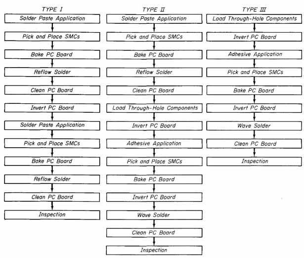
---FIG.—17 Flow charts of process sequence for SMT types I, II, and
III pc boards.
6. DE-SOLDERING FOR SMT
Seldom is the yield 100% where there are no components damaged or solder joint defects after the assembly and soldering process. For SMT, rework and repair is less damaging to the components and the pc board than for conventional through-hole boards. Also, less operator skill is required for working with surface-mounted boards.
De-soldering equipment for SMT falls into two general categories: soldering iron conductive tip configurations and hot air systems. Conductive tips are much less expensive than hot air systems.
In using conductive tips to remove SMCs, all of the solder joints must be melted simultaneously with uniform heat. The component is then removed: first, by a slight twisting and then, by lifting off while the solder is still molten. Twisting is important to prevent damage to the leads, especially if the component is held with adhesive. As the tips heat the solder joints, the adhesive is raised to its glass transition temperature (Tg). This is the temperature at which the adhesive changes from its hardened state to a viscous condition. The twisting motion shears the adhesive. If no adhesive had been used, the twisting is still necessary since it keeps the component flush to the surface of the board as the leads are separated from the molten solder and prevents deforming them.
Some of the common tip styles used for de-soldering SMCs are shown in FIG. 18. FIG..18a shows a tip style designed for leadless chip packages such as ceramic resistors, capacitors, and MELFs. They are also available in widths that will de-solder SOT packages. The tip style shown in FIG. 18b is used on SOIC packages and the arrangement in FIG. 18c is designed for de soldering flatpacks and LCCC and PLCC packages. The tip style selected must have the correct dimensions to span all of the leads of the specific package size.
When using conductive tips for de-soldering, certain precautions must be taken to avoid damage. A liquid RMA flux should first be applied to the solder joints and then the tips placed against the connections with minimum pressure. The length of time for the solder to become molten should not be more than 2 seconds. The tweezer action of the tips, along with their being wetted with mol ten solder, will easily allow the component to be removed from the board. It should then be placed onto a damp sponge and the lands cleaned with a suitable solvent such as isopropyl alcohol. The tips should also be wiped on the sponge to remove excess solder and flux residue.
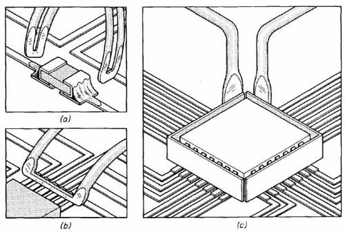
--- FIG.—18 De-soldering tips.
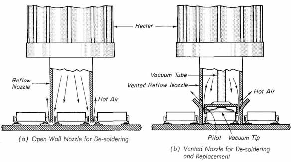
--- FIG.—19 Hot air de soldering systems: (a) open wall nozzle for de
soldering; (b) vented nozzle for de-soldering and replacement.
Hot air systems are available for removal and repair of both passive and active devices. As a result of the special designs of these systems, hot air is directed onto the solder joints through a nozzle. This prevents the bodies of the components from overheating. The temperature reached during the dc-soldering process will be less than that involved in either the vapor-phase or JR reflow operations. The hot air temperatures reach as high as 400°F (205 °C). Two hot air system nozzle designs are shown in FIG. 19. The open wall nozzle shown in FIG. 19a is useful for dc-soldering gull wing style terminations. When fit ted with a precision insert or pilot that fits over the case of the device and a vacuum tube with a suction cup, the system can also be used to remount devices. To remount, a microscope with controls is required to result in perfect lead-to-land registration. Where there is concern for overheating the solder connections of adjacent components that will not be dc-soldered, the vented nozzle design, shown in FIG. 20b, is employed.
Many systems also have the feature of heating the bottom surface of a board in preparation for dc-soldering components on the top surface. The purpose of this is to reduce thermal shock to the board. The temperature used, however, should not be so excessive as to adversely affect bottom surface solder joints or components. Heating the board for 30 to 40 minutes at a tempera ture of 200°F (94°C) has been found to eliminate thermal shock problems while not causing any damage to joints or components.
Exercises:
A. Questions
1 What do the terms SOIC, MELF and PLCC represent?
2 Describe the soldering defect called tombs toning. How is it avoided?
3 How are conventional and SMT components oriented on type II assemblies?
4 What factors govern the selection of solder paste for a specific application? Briefly discuss each factor.
5 What are rheological properties?
6 What are some of the methods used to prevent the formation of solder balls during reflow soldering?
7 What is the difference between pot life and shelf life?
8 What is the advantage to the use of epoxy and acrylic adhesives when compared to the thermoplastic type?
9 Why does a wave soldering system for type II assemblies use a dual solder wave?
10 Why is it recommended to heat the bottom surface of pc boards prior to de-soldering SMCs?
B. True or False
Circle T if the statement is correct, or F if any part of the statement is false.
1 Resistors are much thinner than capacitors and require a longer land to prevent misalignment. T F
2 Lands for MELFs are partially slotted to prevent these devices from rolling out of position when adhesive is not used. T F
3 Type III assemblies have SMCs exclusively on one or both sides of the board. T F
4 Adhesives must be used to hold components and devices to the bottom side of the board for any soldering process used. T F
5 RMA flux is the most active of the three types used in solder paste. T F
6 Solder paste to be deposited by stenciling requires a higher viscosity than that applied by screening. T F
7 When solder paste is applied, a minimum of 75% of the land must be covered. T F
8 Epoxies and acrylics are classified as thermoplastic adhesives. T F
9 Acrylic adhesives require both UV light and heat for curing. T F
10 The maximum soldering iron tip temperature for use on surface-mounted components is 750°F. T F
C. Multiple Choice
Circle the correct answer for each statement.
1 Manually assembled SMCs should be handled by their (bodies, terminations).
2 Plastic SMCs require solder paste having (lower, higher) melting temperatures.
3 Epoxy and acrylics are classified as (thermoplastic, thermosetting) adhesives.
4 Acrylic adhesives can be cured in about (2 hours, 2 minutes).
5 Solder joints should not remain in a solder wave for more than (4, 10) seconds.
D. Matching Columns
Match each item in column A with the most appropriate item in column B.
COLUMN A | COLUMN B
1. Air knife 2. Land pattern 3. MELFs 4. Acrylic 5. Type I assemblies 8. RMA 7. Slump 8. Solder paste |
a. Footprint b. Syringe c. Flux d. Rheologicalproperty e. Round bodies f. SMCs only g. Adhesive h. Wave solder |