
Proper substitution of FETs and SCRs is just as complex a subject as
substitution of bipolar transistors. Here we discuss the characteristics of
SCRs and the many kinds of FETs.
by Bernard B. Daien
In the first part of this article we discussed bipolar transistors, including Darlingtons. It was noted that the frequency response of bipolar transistors can vary considerably, and this factor is important when making substitutions.
SCRs Now we are considering silicon controlled rectifiers briefly, and again, speed is a factor, but the term is changed to, "turn on," and "turn off' time, since the SCR is a latching device.
The SCRs used in some TV sets for horizontal deflection generators, are good examples of this. These SCRs are capable of very fast turn on and turn off times, when compared to the SCRs used for 60 Hertz power line use. Conventional SCRs simply are not fast enough for horizontal sweep use. (The fast SCRs cost considerably more, and are in less abundant supply.) To compound the problem, some TV manufacturers have elected to include a fast damping diode in parallel with the SCR, in the same package. (RCA's "ITR" is one such example). This makes testing a little more confusing. And, of course, the failure of one component requires the replacement of both. The result is that most shops have found it best to replace only with original parts . . . a policy which I recommend.
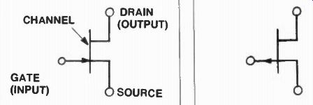
Fig. 1. An N channel Junction FET
Fig. 2. A P channel Junction FET
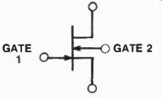
Fig. 3. A dual gate N channel JFET.
SCRs also come in varying sensitivity, so far as the gate pulse amplitude and duration are concerned.
Some devices trigger "on" with microsecond pulse widths, microamperes of gate current, and voltage of a volt or so . . . while others require longer pulses, milliamperes of current, and several volts of amplitude. Again, sensitive SCRs cost more.
Most technicians understand the need for adequate reverse voltage rating, average and peak current ratings, etc. But there is one little characteristic that can give you real headaches . . . the "rate of applied voltage." If an SCR has a very fast rising waveshape applied to the anode, it may turn itself on WITHOUT A TRIGGER PULSE. This characteristic differs with manufacturers, and the particular SCR, and is specified. Often the semiconductor substitution manuals do not even mention this important factor! To sum up, the SCR is as difficult to substitute as most other semiconductors, perhaps even a bit more difficult. Because many consumer electronics service technicians do not have much exposure to SCRs they tend to be cautious about them, which is quite fortunate, in the light of the above mentioned factors.
FETs
FETs come in a wide variety . . . and they are NOT interchangeable, due to different biasing requirements, etc.
The first problem we have is just sorting them out . . . there are two different families, junction FETs (JFETs), and metal-oxide-silicon FETs (MOSFETs). The JFETs and MOSFETs each come in two main varieties, N channel, and P channel (roughly corresponding to the way that bipolar transistors come in NPN or PNP varieties). JFETs and MOSFETs also come in either "single gate" or "dual gate" configurations.
Due to the basic difference in method of operation, JFETs come in only "depletion mode" types, while MOSFETs can be "depletion mode," "enhancement mode," or "enhancement-depletion mode" types.
This set of definitions will be made clear to the reader in the following text, but for now, the point being made is that there is one heck of a lot of FET types . . . and they are NOT interchangeable! It may also come as a surprise that the only way you can identify these different types is by subtle differences in the symbols on the schematic . . . but unfortunately many of the draftsmen who draw electronic schematics are not aware of these differences, so the schematic is often inadequate, or just plain in error when the FETs are depicted. As a result, many textbooks on the subject of semiconductors are also wrong, in the illustrations and schematics provided.
At the present time the industry does not seem concerned about improving the situation, so once again, the service technician must shoulder the burden of doing "detective work" in replacing parts.
I would suggest a rule of thumb that has worked well in the past. If the FET has a standard 'N type part number, such as '3NXXX,' look it up in a semiconductor manual to verify what it is. If the description matches the set function you can then buy it from any distributor under the part number. If it has a non-standard part number (house number), don't waste your time . . . just buy the original part from the set manufacturer." Sorting them out Let's try to sort out the different FETs, in two ways . . . by function, and by schematic symbols. The functions have to be learned, but there are some "tricks" to help identify the schematic symbols. In order to understand how the different FETs function we must first review the theory of operation of JFETs and MOSFETs, very briefly, in a practical way. . . . (Some literature refers to MOSFETs as "insulated gate FETs," or simply IGFETs. They are the same thing.) All FETs, whether JFETs or MOSFETs, operate on the principle of a VOLTAGE INPUT causing the output current of the device to vary, as is the case with vacuum tubes. Stated another way, the input influence is controlled by an electrostatic field, as the electrostatic field around a vacuum tube grid modules the current flowing towards the plate. As in a vacuum tube, the input impedance is very high, since there is no current flow.
The primary difference between the JFET and MOSFET is in how the electrostatic field is created. In the MOSFET the input, called "the gate" is formed by a true capacitor, made by depositing a layer of glass (silicon oxide) on the silicon device, which forms the dielectric of a capacitor. On top of the glass is deposited a metallic layer, forming the second plate of a capacitor. Voltage applied to this plate, causes an electrostatic field to penetrate the dielectric, and influence the flow of current in the silicon. In the JFET the capacitor is not made of metal/oxide/silicon layers, but is made by depositing or forming another silicon layer on the surface of the silicon device, but with doping to form the opposite polarity silicon . . . thus we have N silicon on P silicon (or P silicon on N silicon, as the case may be). This forms a PN junction, which is a semiconductor diode. If we reverse bias this diode, no current will flow, and, in fact, it is a small capacitor! (Remember, a reverse diode is a "varicap.") This capacitor works just like the metal/oxide/silicon capacitor of the MOSFET, with one very important limitation . . . it MUST ALWAYS BE REVERSE BIASED. If it ever becomes forward biased, current will flow, and the input will change from a capacitor to a conductor.
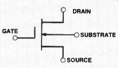
Fig. 4. An N channel MOSFET (depletion mode)
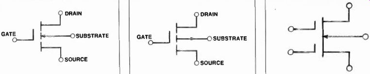
Fig. 5. An N channel MOSFET (enhancement type); Fig. 6. What is this? ; Fig.
7. ... and this?
This means that the input of a JFET can only be reverse biased in some varying degree i e, the current through it can be reduced from the "no input bias" condition, but can never be increased. This is the case with vacuum tubes too . . . and both JFETs and vacuum tubes are said to be "depletion mode" devices, since the output current can be reduced (depleted), but not increased (enhanced) by the application of bias.
In normal use, both the JFET and the vacuum tube are reverse biased by the input bias, in order to get the output current at some operating point, around which the signal input can swing the output current up and down.
Since the MOSFET need not be reverse biased, it is possible to apply either an input bias which increases the output current (forward bias), or a bias which decreases the output current (reverse bias). The MOSFET can thus be biased in either the enhancement mode, or the depletion mode, or in a mode somewhere in between, called the "enhancement-depletion mode." Of course the design of the MOSFET is made to optimize its operation in the intended mode of operation. To sum up then, MOSFETs do not have a limitation on forward bias, as do JFETs.
Freed of this limitation, they can be used in either enhancement or depletion modes of operation ... and therefore the manufacturer of the device can optimize the design for the desired mode of operation.
With these basic facts in mind, let's look at some FET symbols as used (correction, "should be used") in schematic diagrams. Figure 1 shows an N Channel JFET. The polarity of the device, N channel, is indicated by the gate (input) arrow pointing TOWARDS the channel. If you think about it, this is exactly the same symbology used with bipolar transistors, in which the emitter arrow of an NPN transistor points AWAY from the base (P base material). In a PNP transistor the emitter arrow points toward the base (N material). The simple little trick then is to recall that the arrow always points toward N, and away from P material in either bipolar or FET transistors. In the case of bipolars the arrow points towards or away from the base, in the case of FETs it points toward or away from the "channel" (which connects the source and the drain). The drain corresponds to the plate in a vacuum tube, or the collector in a transistor. . . . it is the output terminal in normal usage. Figure 1 also shows that the input is a PN junction formed by the gate and the channel, using conventional diode symbols . . . perfectly clear semiconductor conventional symbology.
Figure 2 illustrated the symbol for a P channel JFET, note the difference between it and the N channel JFET in Figure 1. Figure 3 shows a "dual gate" N channel JFET. This second gate can be used for secondary control purposes, such as AGC. Sometimes dual gate FETs are called "tetrode FETs" but they do not really correspond to tetrode vacuum tubes, and the comparison can be misleading, therefore we will not use it in this article.
Figure 4 shows an N channel MOSFET. Note that the gate capacitor is clearly denoted. In addition, the substrate, which is connected to the channel is shown, and is the means for indicating whether the device is an N channel, or a P channel, by the direction of the arrow. (The substrate is used in all modern MOSFETs, as a result of modern fabrication technology methods.) Actually, this device is a depletion mode device.
Figure 5 shows the same N channel MOSFET as an enhancement device.
Can you spot the difference between Figures 4 and 5? In Figure 5, the channel between source and drain is broken, while in Figure 4 the channel is unbroken.
Look at it as if we are talking about a conductor (which the channel is). If the channel is unbroken it is a good conductor normally. In that case all we can do with the gate is reduce the current, or deplete it . . . so we have a depletion MOSFET. If the channel is pictorially depicted as being interrupted, it symbolizes a poor conductor (open circuit), so that the channel is normally at very low current. In that case, the gate could only be used to increase the current flow (enhance it), and we would have an enhancement MOSFET. Remember, the symbol for the MOSFET depicts the channel as it is normally, without the influence of an external bias applied to the gate.
Obviously external biasing cannot decrease the current through an already open circuit. Similarly it cannot increase the current through an already fully conducting circuit. So, with a moment of thought, you can decipher the clues in the FET symbol.
Let's try our new found knowledge.
Figure 6 depicts a MOSFET. Before reading further, tell yourself what it is . . . . Now let's see what the symbol says. . . . The gate is a capacitor so it is a MOSFET. There is only one gate, therefore, it is not a dual gate device. The substrate arrow points away from the channel . . . indicating a P channel. The channel is interrupted, telling you that it must be an enhancement device because the current can only be made to increase in the channel. Simple, isn't it Similarly Figure 7 is a dual gate, N channel MOSFET, depletion mode.
Did you read it correctly? Now we are adding a little more to the schematic symbol. Since the gate input capacitor can be punctured by static charges, etc., many MOSFETs have added zener diode protection to the input gate. But since destructive input overvoltage can occur in either negative or positive polarity, we need two zeners on the input, reverse polarized with respect to each other.
And to insure that each zener conducts in the proper direction, we add a reverse blocking diode in series with each zener to insure that it works as a zener, and not as a forward diode.
Thus we wind up with four extra diodes in the input, fabricated right along with the MOSFET. Now some schematics omit showing these diodes, in which case it would be very easy to pick up a substitute without zener input protection. So again, you have to be very careful to choose the right substitute . . . and looking up the device number should enable you to determine whether it has input protection or not. Figure 8 shows such an N channel, gate protected, depletion mode, MOSFET. (We are getting a little complicated now!) At this point you can relax, because we have come to the end of the identification part of this FET discussion.
You should now be able to identify what kind of FET you are dealing with, IF the schematic is well drawn. At any rate, you can now read the clues available to you, in making FET substitutions, which is what this article is all about! Figure 9 is a JFET, as indicated by the junction type gates . . . it is a dual gate device, P channel depletion mode. But wait a moment, there are two FETs shown in Figure 9, drawn slightly differently.
The figure is correct . . . it's just that sometimes JFETs are drawn a little differently, depending upon the company making the drawings. I know this can be confusing, but there is no real standardization in the FET field at the present time.
Why so many FETs Think back to vacuum tubes . . . there are diodes, triodes, tetrodes pentodes, pentagrid converters, beam tetrodes, duo diodes, duo triodes, triode pentodes, etc., so we become a little spoiled by the lowly bipolar transistor. FETs come in a variety of types as did vacuum tubes . . . but not quite so wide a variety as tubes.
They have a high input impedance, like the vacuum tubes, which gives us a useful design tool for dealing with high impedance circuits. FETs perform well in AGC'd stages, where transistors do not like to work. So you are going to be seeing more of them now that the technology for making them has been mastered. (They require more stringent manufacturing methods.) FETs also make very good low voltage constant current sources, which gives us a powerful tool for high voltage gains in semiconductor amplifiers. This point is worth a small discussion. . . .
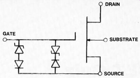
Fig. 8. An N channel protected gate, depletion mode MOSFET. (The diodes usually
are not shown.)
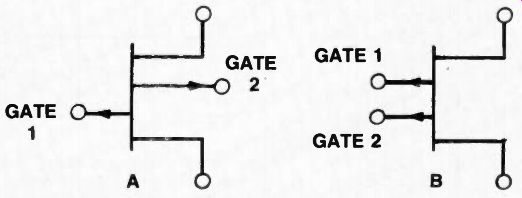
Fig. 9. A dual gate depletion mode, P channel, JFET.
As you already know, even a single transistor amplifier stage can achieve high gain if the load resistor is made very large. The trouble is that a large resistor reduces the collector current to a very low value . . . unless the power supply voltage is increased to a high voltage. This is obviously not practical. One way out of this dilemma is to use a constant current device as a load resistor. A constant current device looks like an almost infinitely large resistor to attempt to change the current flowing through it (it has a very high "dynamic resistance"). If we use a FET as a constant current load, it appears to be a very large resistor, and it is possible to achieve gains of a thousand or more, out of a single transistor stage, at some reasonable value of collector current, and with a low voltage power supply. FFTs are often packaged and sold as "constant current diodes," with the gate tied to the source, forming a two-terminal device. Of course they are not really diodes, but can be connected in the same way a diode is.
Inside of many integrated circuits are such constant current sources, often also called "pinch resistors" because they pinch the current down to some low value. Another name for such constant current sources when used as a load resistor is "active load" (as opposed to resistors which are "passive" loads). Now it is important for you to understand that these "active loads," "pinch resistors," "constant current diodes," or whatever other name you call them by . . . have their current largely determined by the FET characteristics fabricated into them ... and you cannot substitute another FET unless it has substantially identical characteristics.
That should tell you the story about substituting FETs in these applications! Please don't become discouraged, because things could be worse . . . and, as the old cliche goes . . . "Tomorrow they probably will be." It appears that we are in an era where the consumer electronics technician is the forgotten man. The only answer to this problem of "impossible to identify," and "impossible to substitute" devices, is an organized effort to get the set manufacturers to use standard registered parts, available from several of the major manufacturers, and have them clearly identified on parts lists, etc. Until that happens, despite all your efforts, the cost of "detective work" will have to be passed on to the consumer, or absorbed by the shop as a charitable donation to the set maker. The use of non-standard, or "selected" parts is a practice that needlessly complicates the life of the repairman, and should be regarded as very poor manufacturing philosophy which ignores repairability and obstructs the efforts of service technicians.
Before you decide that a FET is bad, check the voltage applied to the device, between the source and the drain. FETs are extremely voltage dependent . . . and strangely enough, an increase in the applied voltage can cause a marked decrease in the current, as the device goes toward the "pinch off" point. This happens because of an internal voltage divider action in the channel, depending upon the geometry of the device i e, where the gate is located along the channel.
An incorrect power supply voltage, changes in the value of associated resistors, etc., which normally would result in relatively minor changes in the current through an ordinary bipolar transistor, can and do cause drastic changes in the current through a FET . . . sometimes even causing the current to completely cut off.
Conversely, substituting another FET with a different "pinch voltage" can cause endless problems. This is like changing from a remote cutoff pentode to a sharp cutoff pentode in a tube type set, only the action is even more pronounced. Put another way, the operating point of the device depends partly upon the biasing, partly upon the design of the device, and partly upon the applied voltage.
As you can see, FETs are a different ball game . . . in use, in design, in symbology, and in troubleshooting. So be careful when you make a substitution . . . Due to the multiplicity of types, and the variations, I recommend that you use an original part whenever possible . . . make substitutions only when there is no other way out. (Except for the registered devices, as previously discussed.) Even with registered devices, some set makers select devices, especially in tuners for FM and TV sets. As usual, in such usage original parts are recommended. FETs are now used in a wide range of frequencies from audio to UHF, and the same precautions apply in their substitution as with the bipolar transistors, so far as application is concerned. Where the frequency is high, and the application is critical, use common sense, and stick with original parts so as to avoid the need for drastic realignment.
This article had as many warnings about what not to do, as suggestions as to what to do . . . but unfortunately that's the way things are in semiconductor substitution. A poor substitute can tie your bench up for hours, because it "works," but not quite right. Once you go through that experience, you will avoid the risky substitutions . . . which is what this article is all about . . . avoiding the risky ones.
(source: Electronic Technician/Dealer)