The field-effect transistor, because it behaves very much like a vacuum tube, opens new approaches to semiconductor circuit de sign. Some circuits in which regular transistors either operate poorly or require special components now operate efficiently and without modification with field-effect transistors.
We can wish that the field-effect transistor had come first. Many transistor circuits then would have- been much simpler than at present, and the transition from tubes to transistors would have been less painful than it was. The regular transistor, as a later development, would have had many special-purpose applications.
Nevertheless, the late coming of the field-effect transistor detracts little from its usefulness.
Field-effect-transistor theory differs somewhat from that of the regular transistor. However, it can be presented in simple terms.
Obviously, the circuit designer functions with increased ease and profit when he understands how this new semiconductor device works. This section presents the necessary elementary theory so that this understanding can be developed.
THE FIELD EFFECT
For more than a century electrical men occasionally pondered the idea of controlling current in a conductor by applying an electrostatic field across the latter. And undoubtedly a great many of them tried it-unsuccessfully. Indeed, sooner or later every experimental-minded schoolboy gets around to mounting a resistor or a length of insulated wire between the plates of a capacitor to see if a voltage applied to the plates will affect the current in the resistor or wire. But no practical device emerged from any early experiments of this kind.
(A) Zero control voltage.
(B) Medium control voltage.
(C) High control voltage.
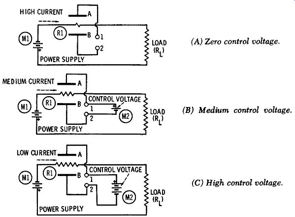
Fig. 1. The field effect.
The electrostatic control which these experimenters sought is appropriately termed the -field effect. This phenomenon is illustrated by Fig. 1. Here A and B are metallic plates parallel to each other and mounted close to, but out of contact with, some sort of resistor ( R1) which is sensitive to an electrostatic field. If a voltage is applied to the plates through terminals 1 and 2, the field set up between the plates penetrates the resistor. A power supply, represented by battery M1, passes current through the sensitive resistor ( R1) and a load resistor ( RL) in series. When the control voltage is zero (Fig. 1A), no field exists between the plates, and resistance R1 is a very low value. Consequently, there is a high current through the load. When a finite control voltage subsequently is applied to the control terminals ( 1, 2), R1 will change and so will the load current. Thus, when the control voltage (battery M2) has some medium value (Fig. 1B ), R1 assumes a somewhat higher value than before, and the load current decreases to a medium level. Similarly, when the control voltage is high ( Fig. 1C), R1 becomes high and the load current is reduced to a low value. If the control voltage is very high, R1 becomes infinite and the load current falls to zero. In this way the load current is modulated by the control voltage. Another way of thinking about the field effect is to suppose that the control voltage decreases the sensitive resistance.
The advantage of such a field-effect device is its voltage-responsive character. That is, ideally no current is drawn from the control-voltage source, although the controlled current may be sizable. This is the same advantage offered by the vacuum tube.
Unlike the tube, however, the field-effect device requires no heater.
The field-effect transistor is the first practical example of such a device.
BACKGROUND OF THE FET
Early searchers for a crystal triode were frustrated in their attempts to use an electrostatic field to modulate current in a semi conductor. They had hoped in this way to imitate the vacuum tube, and their later studies seeking to find out why the arrangement refused to work led to the invention of the regular transistor.
That this transistor became immensely useful is history. But its low input impedance resulted in ( 1) inability to replace the tube in some circuits, ( 2) need for tapped coils and step-down transformers, and ( 3) difficulty for many persons to shift from voltage-amplifier tube thinking to current-amplifier-transistor thinking.
Despite the success of the regular transistor, work continued along the original line. Accordingly, several experimental field-type transistors appeared in the United States and in Europe during the 1950's. (Dr. William Shockley, one of the inventors of the first transistor, reported some of his work along this line in an article, "A Unipolar Field-Effect Transistor," in the November, 1952, issue of Proceedings of the I. R. E.) The modem field-effect transistor ( FET) is the culmination of this continued investigation.
The FET has supplied the high input impedance, through electrostatic control, that was sought by the original researchers. Being more compatible with the vacuum tube than is the regular transistor, the FET gives promise of eventually replacing the tube-and the regular transistor-in many circuits used in electronic equipment.
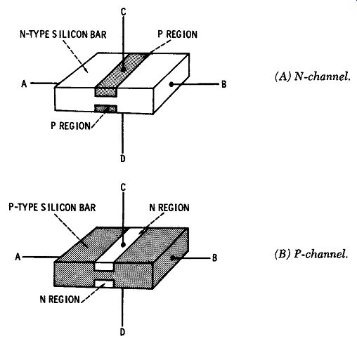
Fig. 2. Basic structure of a field-effect transistor. (A) N-channel. (B)
P-channel.
FET STRUCTURE AND OPERATION
Fig. 2 shows the basic structure of the FET; and while this is not the actual configuration of some commercial models, it is accurate enough for explanatory purposes. The heart of the device is a thin bar or wafer of silicon ( infrequently, germanium) with an ohmic ( non-rectifying) contact ( A, B) at each end. The end-to end electrical path through this bar is termed the channel. If the silicon is N type, as in Fig. l-2A, a P region is processed into each face of the bar in such a way that .each such region is parallel to the other, and a connection ( C, D) is made to each. These regions are termed the gates. (In most commercial FET's, the gates, if two are used, are wired together internally and connected to a single terminal.) The completed transistor is given the name N channel field-effect transistor ( NFET). If, instead, the silicon is P type, as in Fig. l-2B, then the gates are N regions and the transistor is named P-channel field-effect transistor ( PFET). When a d-c voltage is applied between A and B, the current carriers ( electrons in the N-channel and holes in the P-channel FET) flowing through the bar must pass through the channel between the two gate electrodes. The anode terminal (A) is termed the drain, and the cathode terminal ( B) the source. In a symmetrical FET, either terminal may be the source, and the other the drain. The drain is equivalent to the plate of a tube or the collector of a regular transistor; the source is equivalent to the cathode of a tube or the emitter of a regular transistor; the gate is equivalent to the control grid of a tube or the base of a regular transistor.
For FET symbols, see Fig. 3. To emphasize the resemblance of the FET to the tube and to eliminate new terms, some early researchers called the gate, drain, and source by the comparable familiar names of grid, plate, and cathode, but their example failed of adoption.

Fig. 3. FET symbols.
It is the nature of a PN junction that a thin depletion layer is present at the junction. This is a region in which there are no available current carriers. The depletion layer for each FET junction is indicated in Fig. 4 as the region inside the dotted lines at the gate junctions. The depletion layer may be deepened by applying a reverse voltage between the gate and source, the depth increasing with voltage. Such an increase in depth narrows the channel through which the current carriers must pass, thus increasing the resistance of that path.
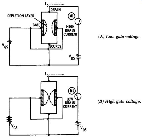
Fig. 4. FET action (N-channel shown).
(A) Low gate voltage.
(B) High gate voltage.
Fig. 4 shows FET action. Here a reverse voltage, Vos, is applied between gate and source. A second voltage, V ns, is applied between drain and source. These are equivalent to the grid and plate voltages, respectively, of a tube. An N-channel unit is shown; for a P-channel, reverse both Vos and Vns, In Fig. l-4A, the shallow depletion layers result from the low gate voltage, and the channel between them therefore is wide ( permitting a large number of electrons to How through the bar), so the drain current, In, is high.
In Fig. 4B, the gate voltage is high and it deepens the depletion layers, causing them to penetrate farther into the bar, narrowing the channel and reducing the drain current. When the gate voltage reaches a critical value, termed the pinch-off voltage, the depletion layers meet, completely shutting off the current. Because the control voltage, Vos, reverse-biases the gate junction, any gate current, loss, is exceedingly tiny ( on the order of 0.1 nano-ampere). This accounts for the high input impedance of the FET and consequently its behavior as a voltage-controlled device. Because the resistance of the silicon bar is modified by the gate-voltage field, the FET is a true field-effect device.
The FET is called unipolar from the fact that it uses only one type of current carrier-majority carriers ( electrons in the N-channel FET's, and holes in the P-channel). Similarly, the regular transistor is called bipolar because it uses both types-majority and minority carriers ( electrons internal, holes injected, in the NPN; holes internal, electrons injected, in the PNP).
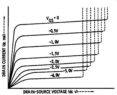
Fig. 5. Typical FET performance curves.
FET PERFORMANCE
The control action in an FET is similar to that in a tube. To illustrate this, Fig. 5 shows a family of curves obtained by varying the drain-to-source voltage, Vos, at various levels of gate-to-source voltage, Vos, and noting the drain current, 10
These curves resemble those of a pentode tube. Note that the avalanche breakdown of the gate junction will be reached if Vos is made high enough.
The sudden increase of drain current at the breakdown point is indicated by the dotted extension of each curve. This breakdown voltage decreases as Vos increases, since Vos acts in series with V Ds to break down the junction.
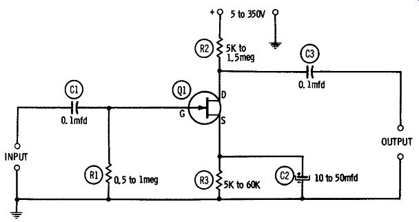
Fig. 6. Typical application (FET audio amplifier).
Because the FET is a voltage amplifier, its performance, like that of a tube, may be rated in terms of transconductance. In the FET, forward transconductance for the common-source circuit ( equivalent to the grounded-cathode tube circuit) is the ratio of a change in drain current to the change in gate-to-source voltage which produces it: where, d I» X 1000 gcs = d-V GS grs is the forward transconductance, in µ.mhos, In is the drain current, in milliamperes, V Gs is the gate-to-source voltage, in volts.
Depending on make, type, and d-c operating voltages of the FET, the transconductance ranges from a low of 35 to a maximum of 50,000 µ.mhos.
The FET lends itself readily to use in tube-type circuits. Fig. 6, for example, shows a common-source audio-frequency amplifier stage. This is equivalent to the grounded-cathode tube-type ampli.6er. The following sections of this book are devoted to the description of such practical circuits.
FET RATINGS
In their data sheets, FET manufacturers give minimum and maximum values of various operating parameters. These include the following, dependent on make and type:
1. Common-Source Forward Transconductance ( gc.). The ratio of din to dV os- Similar to tube transconductance (gm). Given for a specified Vns, Vos, and f = 1 kHz. Range: 35 to 50,000µ.mhos.
2. Common-Source Output Conductance ( Input Shorted) ( g_oss ). Reciprocal of drain-source output resistance. Given for specified V ns, Vos, and f = 1 kHz. Range: 1 to 600 µ mhos.
3. Common-Source Input Capacitance ( Output Shorted) ( C_iss). Capacitance between gate and source. Given for specified V ns, Vos, and f = 1 kHz. Range: 2 to 65 pf.
4. Common-Source Reverse Transfer Capacitance ( Crss). Given for specified Vns, Vos, and f = 1 kHz. Range: 1.5 to 6 pf.
5. Drain Current at Zero Gate Voltage. (I_Dss), The current in the drain-to-source circuit ( i.e., through the channel) when V_GS = 0. Given for specified Vns, Ranges: Vns = 5 v: 0.1 to 10 ma.
Vns = 8 v: 5 to 25 ma. Vns = 10 v: 0.03 to 0.6 ma. Vns = 15 v: 0.2 to 20 ma. Vns = 20 v: 0.4 to 7.5 ma. Vns = 35 v: 80 to 250ma.
6. Drain Cutoff Current ( I_D(oFF) ) . Leakage current through the channel when Vos has been adjusted for output cutoff. Given for specified V ns and Vos, Range ( for V ns of 15 v) : 0.05 na at Vos = 5 v, to 0.07 na at Vos = 10 v.
7. Gate-Drain Voltage (Von), Also called drain-gate voltage. The maximum voltage which may appear between the gate and drain electrodes. Range: 20 to 50 v at 25°C.
8. Gate Reverse Current (loss). Also called gate cutoff current. The reverse current in the gate-to-source circuit. Given for Vns = 0 and a specified V_GS. Range: Vos 15 v: 2 na. Vos 20 v: 10 pa to 0.5 na. V 0 8 30 v: 0.1 to 30 na.
9. Gate-Source Breakdown Voltage (BVoss), The voltage at which the gate junction will enter avalanche. Given for 1 0 = 1 µ.a and Vns = 0. Range: 20 to 50 vat 25°C.
10. Gate-Source Pinch-off Voltage (VP). The gate-to-source voltage at which the field just closes the conduction channel. Given for In = 1 na, 10 na, or 1 µ.a, and a specified V ns ( e.g., 5 to 15 v). Range: 0.6 to 50 v.
11. Gate-Source Voltage (Vos). Also called source-gate voltage. The maximum voltage which may appear between the gate and source electrodes. Range: 20 to 50 v at 25°C.
12. Noise Figure (NF). Internal noise generated. Given for Vos = 0, and a specified V ns ( e.g., 15 v) and frequency ( e.g., 1 kHz, 200-Hz bandwidth). Range: 0.5 to 3 db.
13. Total Device Dissipation ( P). Maximum power which can be safely dissipated by the FET structure. Range: 200 mw to 0.8 w in free air at 25°C.
FET TYPES
It has already been noted that FETs may be classified as N channel or P-channel according to whether N-type or P-type semi conductor material is used in the channel. Alternate terminology is NFET and PFET.
In addition to these two basic types, a newer FET employs a metallic gate which is insulated from the semiconductor by a thin oxide film. This device, which provides an extremely high input impedance because of the near-zero loss and also gives good r-f performance, is known by four names: IGFET ( insulated-gate field effect transistor), MOS (metal-oxide-semiconductor), MOS FET ( metal-oxide-semiconductor field-effect transistor), and MOST ( metal-oxide-semiconductor transistor). The symbol for this FET is given in Fig. 3C.
Another development is the tetrode FET. This unit has two gate terminals ( "front gate" and "back gate") and its symbol is given in Fig. 3D. The tetrode, which acts like a variable-pinch-off FET, provides a high g_fs/C_gss ratio and consequent superior performance as a radio-frequency amplifier.
[Note: This guide is based on Sams "FET Circuits", pub'd in 1961]