AMAZON multi-meters discounts AMAZON oscilloscope discounts
THE first widespread practical application of transistors was in audio amplifiers. The reason for this is easy to understand when it is remembered that the early transistor essentially was a low-frequency device. Its small size, low dc voltage and current requirements and high efficiency suit the transistor naturally to use in hearing aids, which are small-sized audio amplifiers.
Since the early developmental period, great progress has been made in the design and manufacture of transistors and allied circuit components and in amplifier circuit design. Numerous circuits have been offered to the engineer, technician and hobbyist.
Representative audio-amplifier circuits are described in this section.
Single-stage, R-C-coupled, common-base amplifier Fig. 101 shows the circuit of a single-stage resistance-capacitance coupled amplifier employing the common-base configuration. This circuit sometimes is called "grounded base." This amplifier provides a voltage gain of 30 when operated into a high-impedance load. Power output is 1.8 milliwatts. Its input impedance is 130 ohms and output impedance 5,000 ohms. The maximum input signal voltage which may be applied before output-voltage peak clipping appears is 0.1 volt rms. The corresponding maximum output signal voltage is 3 volts rms. Fig. 102 shows the frequency response.
Two batteries are required in the common-base amplifier, B1 (1.5 volts) for the emitter bias and B2 (6 volts) for collector bias. Battery B2 supplies approximately 0.8 milliampere dc and battery B1,0.85 ma. The dpst switch (S1-S2) makes and breaks connections to both batteries simultaneously.
An alternative, single-battery circuit is shown in Fig. 103. Here, a voltage divider R3-R4 is operated with a single 7.5-volt battery.
Current flowing through the divider develops the emitter voltage as a drop across R3 and collector voltage across R4. The bleeder current is 9.62 ma.
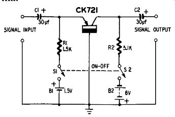
Fig. 101. Single-stage, R-C-coupled, common-base amplifier.
All resistors in Figs. 101 and 103 are 1/2 watt.
Capacitors C1 and C2 may be miniature, low-voltage tantalum electrolytics if subminiaturization is desired.
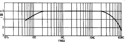
Fig. 102. Frequency response of single stage, R-C-coupled, common-base amplifier.
Single-stage, transformer-coupled, common-base amplifier
In any transistorized amplifier, the highest per-stage power gain is obtained only with transformer coupling between stages or between input and output.
Fig. 104 shows the circuit of a typical common-base, transformer coupled, single-stage amplifier employing a General Electric 2N45 transistor. This amplifier has been designed for 50,000 ohms input impedance and 500 ohms output impedance. Power output is 2 milliwatts and power gain is 500 times, or 27 db. This means that an input-signal driving power of 4 microwatts will give full output.
Miniature transformers are employed for input (T1) and output (T2) coupling. If these transformers are mounted close together, they must be oriented in such a way that their cores are at right angles to prevent feedback.
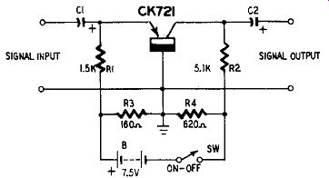
Fig. 103. Alternative arrangement using single battery and voltage divider.
Bypass capacitors C1 and C2 may be standard 25-volt electrolytics or miniature tantalum electrolytics. Variable resistor R is a 2,000-ohm miniature wirewound rheostat. Initially, this control is set for a dc collector current of 1 milliampere.
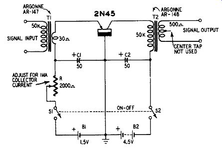
Fig. 104. Single-stage, transformer-coupled, common-base amplifier.
Single-stage, R-C-coupled, common-emitter amplifier
The common-emitter circuit, also called grounded-emitter, provides high voltage and high power gain and is adapted readily to single-battery operation.
Fig. 105 gives the circuit of a single-stage, R-C-coupled, common-emitter amplifier employing a Sylvania 2N34 transistor. Fig. 106 shows its frequency response. The input impedance, measured at 1,000 cycles, is 780 ohms; the output impedance 10,000 ohms. The voltage gain is 80 when the amplifier is operated into a high-impedance load. (Higher values of gain may he obtained with individual transistors.) Maximum input-signal voltage before output voltage peak clipping is 20 millivolts rms. Corresponding maximum output-signal voltage is 1.7 volts rms. Total current drain is 500 microamperes dc.
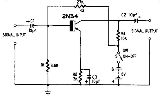
Fig. 105. Single-stage, R-C-coupled, common-emitter amplifier.
The transistor operating point is stabilized by the steady value of base bias voltage supplied by voltage divider R1-R3 and emitter resistor R2. The latter is bypassed by capacitor C3 to prevent degeneration.
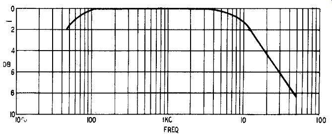
Fig. 106. Frequency response of circuit shown in Fig. 105.
The electrolytic coupling capacitors C1 and C2 and bypass capacitor C3 may be standard-size 25-volt components or miniature, tantalum electrolytics.
Single-stage, transformer-coupled, common-emitter amplifier
Transformers are employed for input and output coupling in the common-emitter circuit shown in Fig. 107. This allows very nearly the full 39-db power gain of the transistor (Raytheon CK722) to be obtained.
Miniature transformers are used. While the 200-ohm secondary of T1 and the 15,000-ohm primary of T2 do not match the transistor input and output impedances exactly, the match is close enough for good power transfer. The secondary of T2 may be connected directly to the base-input circuit of a similar amplifier stage.
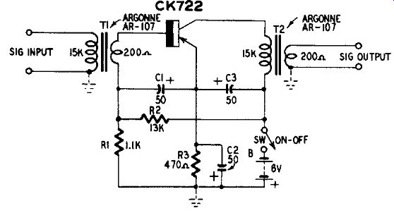
Fig. 107. Single-stage, transformer-coupled, common-emitter amplifier.
Dc base bias is supplied by the R1-R2 voltage divider. Further stabilization of the operating point is provided by emitter resistor R3 which is bypassed by C2 to prevent degeneration.
Single-stage, R-C-coupled, common-collector amplifier
The common-collector circuit (also known as the grounded collector) has the highest input impedance of the three transistor amplifier configurations. Its operation and characteristics resemble somewhat those of the vacuum-tube cathode follower and, for this reason, the common collector often is referred to as an "emitter follower."
Fig. 108. Single-stage, R-C-coupled, common-collector amplifier.
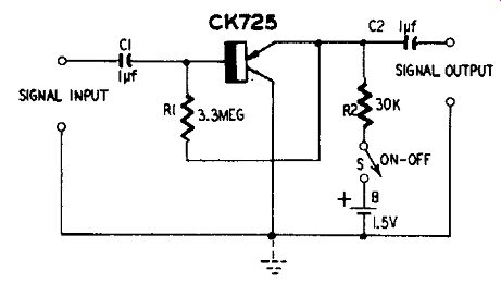
Fig. 108 shows a single-stage, resistance-capacitance-coupled, common-collector
amplifier employing a Raytheon CK725 transistor. At 1,000 cycles, the input
impedance of this amplifier is 1 megohm. Output impedance is 30,000 ohms. The
input impedance varies with the signal frequency, being 1.2 megohms at 20 cycles
(Fig. 109-a) and 160,000 ohms at 50 khz.
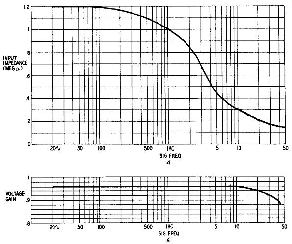
Fig. 109-a,-b. Characteristics of common-collector amplifier: (a) input impedance
variation; (b) frequency response.
The voltage gain of the amplifier is constant at 0.96 from 20 cycles to 10 khz (Fig. 109-b) and falls slowly to 0.88 at 50 khz. The maximum input-signal voltage before positive-peak clipping appears in the output signal is 0.52 volt rms. The corresponding maximum output-signal voltage is 0.499 volt rms when the external load is 300,000 ohms or higher. Power gain is 30.74, corresponding to 14.87 db.
Single-stage, transformer-coupled, common-collector amplifier
The common-collector amplifier is convenient for coupling into a low-impedance line. However, Z1 varies with the output impedance (Z0) , with the result that Z1 drops to approximately 20,000 ohms when Zo = 500 ohms.
The most satisfactory operating conditions therefore are obtained when the common-collector output is transformer-coupled to the lower-impedance line. Fig. 110 shows a common-collector amplifier with transformer output. Here, the input impedance follows the curve given in Fig. 109-a and the output impedance is constant at 100 ohms.
The common-collector amplifier may be transformer-coupled to the base-input circuit of a common-emitter amplifier by employing a transformer having a 1,000-ohm secondary.
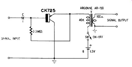
Fig. 110. Single-stage, transformer-coupled, common-collector amplifier.
Multistage R-C-coupled amplifier Fig. 111 shows the circuit of a four-stage, resistance-capacitance coupled amplifier employing Sylvania 2N34 transistors. Each stage utilizes the common-emitter circuit.
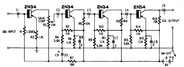
Fig. 111. Multistage R-C- coupled amplifier.
With the GAIN CONTROL set at maximum, this amplifier provides a voltage gain of 4,000. The maximum input-signal voltage before output-voltage peak clipping is 0.2 millivolt rms. The corresponding maximum output-signal voltage is 1.2 volts rms. At 1,000 cycles, the input impedance is approximately 1,000 ohms. The noise level was measured as 5 millivolts, with the input terminals of the amplifier short-circuited (72 db below maximum output voltage) . Fig. 112 shows the frequency response.
Stabilizing bias is applied to the bases of the transistors by voltage divider networks R4-R5, R9-R10 and R13-R14. To prevent de generation, emitter resistors R6, R11 and R15 are bypassed by capacitors C6, C7 and C8. Emitter resistor R2 in the input stage is left unbypassed for a small amount of degeneration in this stage.
Capacitor C9 and resistor R7 form a decoupling network to suppress motorboating.
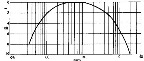
Fig. 112. Frequency response of the circuit shown in Fig. 111.
Total current drain is approximately 8 milliamperes dc from the 6-volt battery.
Multistage transformer-coupled amplifier
A three-stage transformer-coupled amplifier employing Raytheon CK722 transistors is shown in Fig. 113. This circuit provides an overall power gain of 80 db (with GAIN CONTROL R5 set to maximum) and a power output of 6 milliwatts. The input impedance is approximately 1,000 ohms and the output impedance 1,200 ohms.
The dc base bias is stabilized in each stage by means of voltage dividers R1-R2, R6-R7 and R9-R10. Emitter current-limiting resistors R3, R8 and R11 are bypassed adequately by C2, C5 and C7 to prevent degeneration. Capacitor C3 and resistor R4 form a de-coupling network to suppress motorboating. The total current drain from the 3-volt battery is 7.3 milliamperes dc.
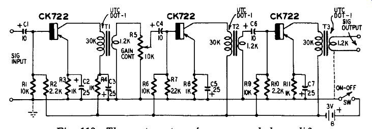
Fig. 113. Three-stage transformer-coupled amplifier.
In the construction of this amplifier, the miniature transformers T1, T2 and T3 must be mounted far enough apart that their magnetic fields do not interact. When a compact layout necessitates close spacing, the transformers must be oriented in such a way that their cores are at right angles.
Push-pull output circuits
As in vacuum-tube practice, push-pull output amplifier stages and drivers are employed when more signal power is desired than can be supplied by a single-ended transistor stage. Fig. 114 shows typical class-A and class-B push-pull output stages.
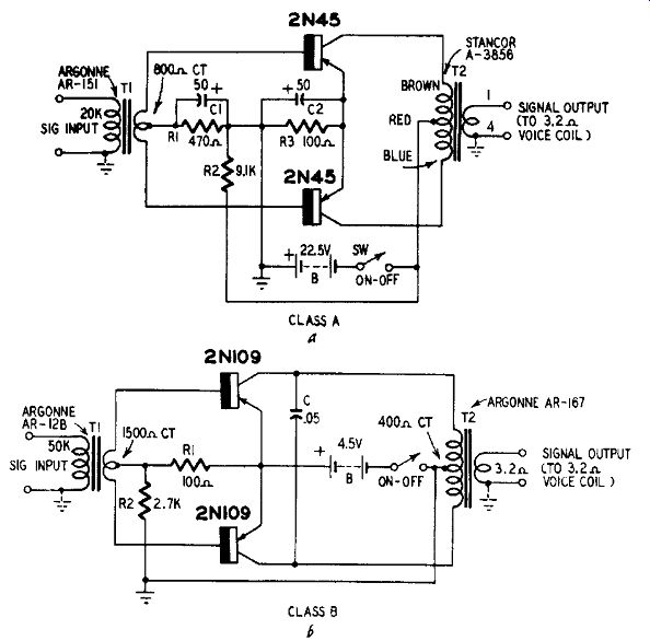
Fig. 114-a,-b. Push-pull amplifiers: (a) class A; (b) class B.
Class A
(Fig. 114-a) .
Here, two General Electric 2N45 transistors are employed. The input impedance is 20,000 ohms. (The 20,000-ohm primary of the input transformer T1 can act as the collector load of a single-ended transistor input stage.) The output impedance matches the 3.2-ohm voice coil of a loudspeaker. At 5% total harmonic distortion (measured at 1,000 cycles) , the power output is 75 milliwatts and the overall power gain 30 db, or 1,000 times.
The total continuous current drain is 12 milliamperes dc from the 22.5-volt battery. The collector-circuit efficiency is 42%. Stabilizing dc bias is supplied to the bases of the transistors by the voltage divider R1-R2. The emitter current-limiting resistor R3 is by passed by C2 to prevent degeneration.
Class B
As in tube practice, class-B transistor output amplifiers are preferred to class-A units because of their higher collector-circuit efficiency. In the class-A circuit (Fig. 114-a) , a rather large collector current flows continuously, while in class-B circuits large values flow only on audio peaks and at other times the "resting" collector current is negligible.
Fig. 114-b shows a typical class-B circuit employing two RCA 2N109 transistors. The input impedance of this amplifier is 50,000 ohms and the output impedance 3.2 ohms to match the voice coil of a loudspeaker. At approximately 8% total harmonic distortion (measured at 1,000 cycles) , the power output is 75 milliwatts and overall power gain is 30 db, or 1,000 times. The collector-circuit efficiency is 64%.
The zero-signal total collector current is approximately 4 ma dc, and the maximum-signal total collector current approximately 26 milliamperes. The base-bias voltage divider R1-R2 draws approximately 1.6 milliamperes.
Phase inverters
The interesting properties of transistors permit the design of ingenious phase inverter circuits. Fig. 115 shows two types.
Single-transistor type (Fig. 115-a) .
This is a simple circuit employing one Raytheon CK721 transistor and is similar to the so-called "hot-cathode" phase inverter sometimes used with triode vacuum tubes. A portion of the output-signal voltage (OUTPUT 1) is developed across the collector load resistor R4 and a second portion (OUTPUT 2) across the emitter resistor R3. Due to phase shift, which is inherent in the common-emitter circuit, OUTPUT 1 is out of phase with the input-signal voltage while OUTPUT 2 is in phase with the input. The two output-signal voltages accordingly are out of phase with each other.
A 20-millivolt rms input-signal voltage will give output voltages of approximately 0.8 volt when the phase inverter feeds into high-impedance loads. Actually, these two output voltages are not exactly equal because the circuit is not perfectly balanced. However, they may be made very nearly equal by adjustment of R3 either above or below the specified 4,700-ohm value, as required.
Complementary-symmetry type
The circuit shown in Fig. 115-b makes use of the principle of complementary symmetry which is evidenced when n-p-n and p-n-p transistors with identical characteristics (other than polarity) are operated in the same circuit. The n-p-n unit here is a Sylvania 2N35 and the p-n-p a Sylvania 2N34.
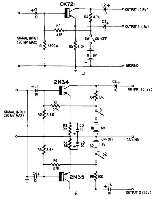
Fig. 115-a,-b. Phase inverters: (a) single-transistor type; (b) complementary-symmetry
type.
Notice that the circuit above the ground line is identical with that below the line except for the transistor type and the polarities of batteries and capacitors. Since the input circuits of the two halves are connected in parallel, the input signal is applied in the same phase to each transistor. The two output signals (OUTPUT 1 and OUTPUT 2) are out of phase with each other.
When a signal is applied with the same polarity to an n-p-n and p-n-p transistor simultaneously, the collector currents shift in opposite directions. Thus in Fig. 115-b, when the upper SIGNAL INPUT terminal is made positive with respect to the lower terminal, the 2N34 collector current decreases while the 2N35 collector current increases. The 2N34 collector therefore becomes more negative, while the 2N35 collector becomes more positive. OUTPUT I accordingly swings negative while OUTPUT 2 swings positive. These conditions reverse when the upper INPUT SIGNAL, terminal is made negative.
The maximum value of input-signal voltage before peak clipping in the output signal is 20 millivolts rms. The corresponding maximum output-signal voltage is 1.7 volts rms each for OUTPUT 1 and OUTPUT 2.
The two output-signal voltages may be equalized by matching the transistors, circuit components, and battery voltages closely.
Base-bias stabilization is provided by voltage dividers R1-R2 and R5-R6.
Class-B loudspeaker amplifier with conventional transistors
Useful loudspeaker operation may be obtained with transistorized power amplifiers. Fig 116 shows a two-stage amplifier circuit employing small, conventional transistors.
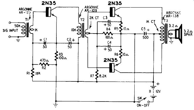
Fig. 116. Class-B loudspeaker amplifier with conventional transistors.
N-p-n transistors ( Sylvania 2N35) are used both in the single-ended class-A driver and push-pull class-B output stages. Operated from a 12-volt battery, this amplifier delivers 100 milliwatts of audio power to the loudspeaker. Input power is 0.25 microwatt.
This represents an overall power gain of 56 db, or 400,000 times.
Full audio output is obtained with an input signal voltage of 112 millivolts rms. Total harmonic distortion at 1,000 cycles is 5 % .
Input impedance of the amplifier is 50,000 ohms. This permits the unit to be driven by high-impedance microphones, phonograph pickups, or transistorized preamplifiers.
Total zero-signal current drain is 10 ma dc from the 12-volt battery. Total maximum-signal current is 23 ma. Stabilizing base bias is supplied by the voltage-divider networks R1-R2 and R4-R7. Divider resistors RI and R7 may require adjustment for optimum performance, especially for the elimination of crossover distortion.
Class-B loudspeaker amplifier with power transistors When the desired amount of audio power exceeds the capability of conventional transistors, power transistors are required.
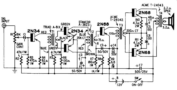
Fig. 117. Class-B loudspeaker amplifier with power transistors.
Fig. 117 shows the circuit of a complete amplifier employing conventional transistors in the low-level stages and power transistors in the driver and class-B output stages. With the GAIN CONTROL, R1 set to maximum, this amplifier delivers an output power of 5 watts to the voice coil of a 3.2-ohm loudspeaker. For full audio output power, the input-signal voltage is 1 millivolt rms. Overall power gain is 68 db. Noise level is 6 my (56*db below maximum output voltage) and total harmonic distortion at 1,000 cycles is 11%. Fig. 118 shows the frequency response.
Common emitters are used throughout. The first stage employs a Sylvania 2N34 as a class-A amplifier. The second stage employs push-pull 2N34's in class A. The third stage is the class-A driver with a Sylvania 2N68 power transistor. The output stage employs two 2N68's operated in push-pull class B.
The 2N68 driver draws a steady dc collector current of 150 ma.
The total zero-signal collector current of the push-pull output stage is 1.5 milliamperes dc and the total maximum-signal collector current 550 ma dc.
To dissipate the heat generated during operation, all three power transistors must be bolted solidly to the metal chassis of the amplifier. However, they must be insulated from the chassis electrically, since their cooling structures are at collector potential. This is accomplished by using a 1.5-mil-thick mica washer between the transistor case and the chassis.
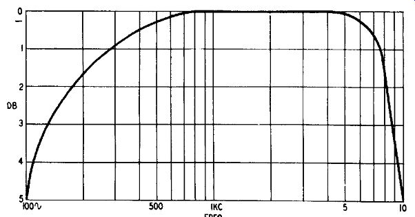
Fig. 118. Frequency response of Class-B loudspeaker amplifier with power transistors.
Class-A loudspeaker amplifier with power transistor
A power transistor operated as a class-A amplifier does not provide as high output as when a pair are operated class B, but the class A power type gives considerably more power than conventional transistors even when the latter are operated class B.
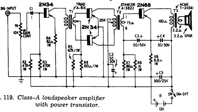
Fig. 119. Class-A loudspeaker amplifier with power transistor.
Fig. 119 shows the circuit of an amplifier in which the output stage contains a single class-A-operated Sylvania 2N68 power transistor. The audio output of this amplifier is 0.6 watt. The two low level stages employ Sylvania 2N34 transistors (single-ended in the input stage and push-pull in the intermediate stage).
Full output power is obtained with a 1-millivolt rms input signal. Total continuous current drain is 200 milliamperes dc from the 12-volt supply. Dc base-bias stabilization is provided by voltage-divider networks R2-R3, R5-R6 and R7-R8. Emitter resistor R4 in the input stage is left unbypassed for degeneration.
Complementary-symmetry power amplifier with conventional transistors The principle of complementary symmetry, explained in connection with the n-p-n-p-n-p phase inverter (Fig. 115-b and its accompanying section) may be utilized to obtain a novel single-ended push-pull amplifier.
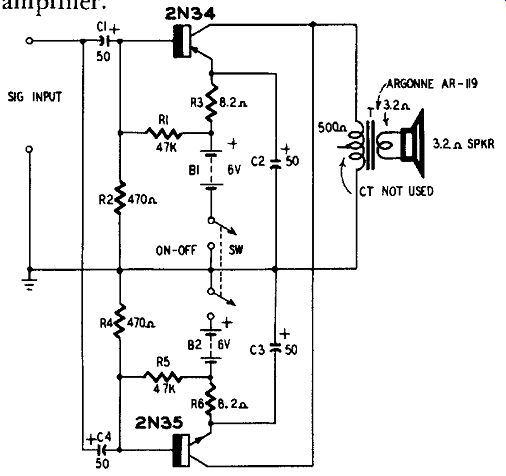
Fig. 120. Complementary-symmetry power amplifier with conventional transistors.
Fig. 120 shows the circuit of a complementary-symmetry class-A amplifier employing conventional small-sized transistors. This unit has an audio power output of 100 milliwatts. Its power gain is 40 db. For full output, the input-signal driving power is 0.01 mw. In put impedance is approximately 400 ohms.
This circuit employs a Sylvania 2N34 transistor as the p-n-p unit and a Sylvania 2N35 as the n-p-n. Notice that the halves of the circuit above and below the ground line are images of each other, except for the differences in transistor type and of the polarities of batteries and capacitors.
If the transistors, battery voltages and resistors are matched care fully, the circuit will be balanced and no dc can flow through the primary winding of output transformer T. This transformer there fore can be less expensive than one intended to carry dc. (A 500-ohm voice coil could be connected directly into the circuit without a coupling transformer) .
The complementary-symmetry circuit is unique in that, although it provides true push-pull action, both its input and output circuits are single-ended. Thus, no phase inverter is required at the input nor is a center-tapped output transformer needed. Its single disadvantage is that it requires two batteries, B1 and B2. However, a single tapped battery can be used.
Complementary-symmetry power amplifier with power transistors Fig. 121 is the circuit of a class-B complementary-symmetry amplifier employing power transistors and having an output of 5 watts.
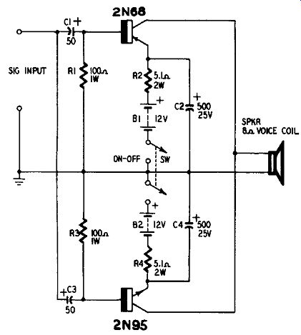
Fig. 121. Complementary- symmetry power amplifier with power transistors.
The p-n-p transistor is a Sylvania 2N68 and the n-p-n unit a Sylvania 2N95. Two 12-volt batteries are employed although a single tapped 24-volt battery might be used. Total zero-signal collector current is 1 ma dc and the total maximum-signal collector current 550 ma dc.
These values are for the two transistors; the per-transistor values are 0.5 and 275 ma.
The input impedance of this amplifier is approximately 20 ohms.
Overall power gain is 12-15 db. The input-signal driving power is 168 milliwatts.
The low output impedance of the amplifier is reasonably close to matching the 8-ohm voice coil of the loudspeaker. It is safe to connect this voice coil directly into the circuit without an output trans former, as shown, since the circuit is balanced and no dc can flow through the speaker if the transistors, battery voltages and resistors are matched carefully. If the transistors are nearly, but not exactly, matched some degree of matching may be secured by varying either R2 or R4 to balance the circuit, like a bridge, and remove any dc from the voice coil.
Single-stage low-noise preamplifier
The single-stage preamplifier circuit shown in Fig. 122 employs a Raytheon CK727 transistor, a low-noise type. It is particularly important to have a quiet preamplifier when the main amplifier following this unit has considerable gain,
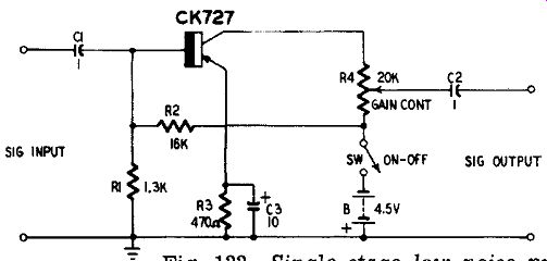
Fig. 122. Single-stage low-noise preamplifier.
Having an input impedance of approximately 1,000 ohms, this circuit provides a voltage gain of 93 with the GAIN CONTROL R4 set to maximum. The maximum input-signal voltage before output-signal peak clipping is 10 millivolts rms. The corresponding maximum output-signal voltage, across a high-impedance load, is 0.93 volt rms. Fig. 123 shows the frequency response.
The noise voltage, measured with an ac vacuum-tube millivolt-meter at the amplifier output terminals, was 3 millivolts with the amplifier input terminals short-circuited. This is 49.8 db below maximum output signal voltage.
The total drain from the 4.5-volt battery is 360 microamperes dc.
Preamplifier with high-impedance input
Through the use of a common-collector input stage, the pre amplifier circuit shown in Fig. 124 achieves high input impedance.
This is an invaluable property when the amplifier must impose negligible loading upon the signal source from which it is operated. The final stage also employs the common-collector circuit to provide the low-impedance output of 500 ohms while maintaining a fairly high input impedance.
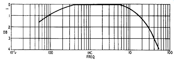
Fig. 123. Frequency response of the low-noise preamplifier.

Fig. 124. Preamplifier with high-impedance input.
Like vacuum-tube cathode followers, common-collector transistor amplifiers have voltage gains of less than 1. The gain of this pre amplifier therefore is supplied by an intermediate common –emitter stage. Although the common-emitter and common-collector circuits require dc bias voltages of opposite polarity, use of a single battery has been made possible in this preamplifier circuit by operating an n-p-n transistor (Sylvania 2N35) in each of the common collector stages and a corresponding p-n-p transistor (Sylvania 2N34) in the common-emitter stage.
At 1,000 cycles, the measured input impedance of the preamplifier is 0.2 megohm. Higher values, up to 1 megohm or better, may be obtained through a special selection of the input transistor. Maximum input-signal voltage before output-voltage peak clipping is 4 millivolts rms. Corresponding maximum output voltage is 0.2 volt rms. Voltage gain is 50 times, or 34 db. Power is 56 db. Total harmonic distortion at 1,000 cycles is 1.2e,. Fig. 125 shows the frequency response.
Total drain from the 6-volt battery is 600 microamperes dc. This low power drain of the preamplifier, together with the small number of components and the absence of transformers, permits miniature construction (e. g., mounting in a probe handle) and operation from penlight batteries or photoelectric cells.
If a gain control is required, a 15,000-ohm potentiometer may be substituted for the 15,000-ohm load resistor R3.

Fig. 125. Frequency response of preamplifier.No bias-stabilization networks
have been provided in this pre amplifier. These resistors were omitted to reduce
the number of components, minimize the dc drain and keep the input impedance
of each stage as high as possible. (The input and output stages have "floating" bases
for highest input impedance) . The lack of stabilization limits the amplifier
to use in reasonably constant temperature environments and to low signal-input
voltage levels (not exceeding the 4-mv value mentioned earlier).
Boosting transistor input impedance
Experimenters find it hard to make transistors work "like tubes" in some circuits because the input impedance of the transistor inherently is low while that of the tube is very high. The input impedance of a transistor amplifier might be 1,000 ohms or less while a tube amplifier may exhibit several megohms.
In a transistor amplifier, this difficulty may be overcome to some extent by using a stepdown input transformer. This gives the amplifier a much higher input impedance than it could offer alone. But the use of a transformer is not desirable in every case, simple resistance-capacitance coupling sometimes being preferred even to a subminiature transformer.
Three schemes for boosting transistor input impedance without a transformer immediately come to mind. One of these is to add a series resistor to the transistor input circuit, the second is to em ploy emitter degeneration (obtained by means of an unbypassed resistor in series with emitter and ground in a common-emitter circuit) and the third is the common-collector type of amplifier circuit which normally has many times the input impedance of the more widely-used common-emitter circuit. Each of these schemes has its place, and it is interesting to compare these circuits with the conventional common-emitter.
Fig. 126-a shows the common-emitter circuit used for comparison on a basis of experimental operation. The measured input impedance is 1,500 ohms and the voltage gain is 100. The value of the collector resistor R2 was chosen experimentally, with the individual transistor, for maximum voltage gain.
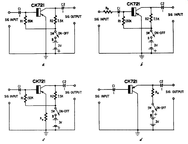
Fig. 126. (a to d). (a) original common-emitter circuit; (b) series resistance;
(c) emitter degeneration; (d) common collector.
Series-resistance method
The first step was to add series input resistance to the original common-emitter circuit. Thus, R, was inserted as shown in Fig. 126-b. The presence of R. reduces the amplification of the stage. It was found that when R. = 1,500 ohms, the input resistance of the stage is 3,000 ohms and the voltage gain drops to 50, just one-half of its original value. When R, is increased to the point at which the gain is reduced to 1, similar to the ideal gain of a cathode follower; R, = 90,000 ohms, the input resistance of the stage is 91,500 ohms and the voltage gain is 1. Obviously, there is no voltage amplification in this instance; but there is a power amplification of 25, since the output impedance is less than the input impedance.
Thus, various values of added resistance R8 between 1,500 and 90,000 ohms boost the original input resistance (impedance) by 2 to 61 times, but at the same time they reduce the voltage gain to a value from 0.5 to 0.01 of its original level.
Emitter degeneration method In the common-emitter circuit, an unbypassed resistor inserted between emitter and ground will provide degeneration which raises the input impedance of the circuit. An interesting fact to note is that the resulting input impedance is higher than the value of the added resistor, and the voltage gain of the basic circuit is not lost nearly as fast as when using an ordinary series input resistor. Fig. 126-c shows connection of the emitter series resistor Re into the original circuit.
Table 1 shows how the input resistance Rin and voltage gain vary with the value of the emitter resistance Re. These values will differ somewhat with individual transistors.

Table 1-Input and Emitter Resistance vs. Voltage Gain
Voltage Gain
Common-collector circuit
In the common-collector amplifier circuit, the collector is the grounded or common electrode of the transistor and the emitter be comes the output electrode. The common collector normally has the highest input impedance of the three basic transistor circuits. It has somewhat less power gain than the common emitter and common base. Fig. 126-d shows the common-collector circuit tested.
Emitter resistor Re was varied for maximum voltage gain, which was found to be 0.90. At this point, Re = 20,000 ohms and the input resistance (impedance) is 0.5 megohm.
Analysis
A number of conclusions can be drawn from these simple results.
The alert experimenter may find several applications for each of the three circuits in which the input impedance has been boosted. The analysis runs somewhat as follows.
1. If there is gain to spare and the input impedance need be raised only a small amount, use Fig. 126-b. Resistor R. may be inserted on either side of capacitor C1.
2. If the voltage gain must be kept as high as practicable and still a relatively large increase in input impedance obtained, use Fig. 126-c.
3. If the highest possible input impedance is required and a voltage gain of less than 1 can be tolerated, then use the emitter follower Fig. 126-d.
4. With regard to frequency response, Fig. 126-d has the best (excellent) , Fig. 126-c next best (good) and Fig. 126-b the worst (fair to poor, depending upon how high a value of Rs is employed) .
REFERENCES
1. Rufus P. Turner, Common-Collector Transistor Amplifier. RADIO-ELECTRONICS Magazine, September, 1955; p. 37.
2. Rufus P. Turner, 5-Watt Transistorized Audio Amplifier. Radio & Television News, April, 1956; p. 53.
3. Rufus P. Turner, Low-Noise Transistor Preamplifier. RADIO-ELECTRONICS Magazine, August, 1954; p. 64.
4. Rufus P. Turner, Transformerless Line Output Preamplifier. Electronics, August, 1956; p. 198.