AMAZON multi-meters discounts
AMAZON oscilloscope discounts
MANY of the modern applications of electronics utilize pulse techniques. In contradistinction to early communication-type circuits which handled signals having only sinusoidal or near-sinusoidal waveforms (although often of varying amplitude or frequency) , pulse circuits are characterized by abrupt on-off (switching) operation and frequently depend upon the phase relation between two or more signal pulses to secure a desired result. These techniques are employed in computers, counters, radar, television, automation, industrial electronics and in some test instruments.
Some pulse-type equipment employs large numbers of vacuum tubes with the attendant problems of size, power demand, heat removal, circuit complexity and unreliability. Considerable attention accordingly has been directed toward the transistor-a small-sized, rugged and dependable component requiring only tiny amounts of operating power, generating negligible heat, endowed with long life and providing high power gain.
Much of the transistorized pulse circuitry which has been developed is highly specialized and without wide general interest, especially to the hobbyist. The few circuits which appear in this section have been selected as representative building blocks illustrating the transistorization of well-known pulse systems and having some application value to general experimenters.
Flip-flop
Fig. 701 shows the circuit of a transistorized flip-flop comparable to the Eccles-Jordan vacuum-tube circuit. Like its counterpart, this is a bistable on-off circuit delivering one output pulse for each pair of successive input pulses. This feature suits the flip-flop as a basic scale-of-2 counter or frequency halver. For fast rise and fall times in the output pulse, rf transistors ( Sylvania 2N94A) having 6- mhz cutoff are employed.
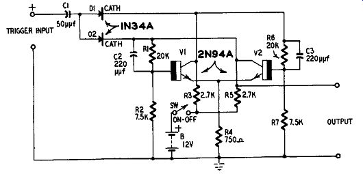
Fig. 701. Flip-flop circuit.
When the circuit is operating, either V1 or V2 is conducting collector current while the opposite transistor is cut off. Thus, a pulse is delivered to the OUTPUT terminals only when V2 conducts.
A second, separate output terminal could, of course, be connected to the collector of V1. Output pulses then would be delivered alternately by the two pairs of output terminals as conduction shifted between V1 and V2.
Conduction is switched from one transistor to the other by means of a positive trigger pulse applied to the TRIGGER INPUT terminals.
Application of this pulse causes the off transistor to switch on and the on transistor to switch off.
Operation of the circuit is explained in the following manner:
When switch SW is closed, both transistors will start to draw collector current through collector load resistors R3 and R5, respectively.
However, because of random transients (perhaps due to noise components in currents) , the collector current of one transistor will increase, although this action may be only momentary. If this occurs in V1, for example, the increased collector current will produce a rise in the voltage drop across R3 and this will lower the V1 collector voltage. This change is coupled across to the base of V2 through the voltage divider R6-R7 and this action lowers the V2 base voltage. As a result, the collector current of V2 decreases and this causes the collector voltage of V2 to increase. This increase is coupled through voltage divider R1-R2 to the base of V1 and acts to increase the V1 collector current still more. The action now continues rapidly in this direction until V1 is conducting heavily (low collector voltage) and V2 is cut off (high collector voltage) .
The action is completed in a rapid flip. This is one of the stable states of the circuit and will be preserved until switch SW is opened momentarily or conduction is shifted from V1 to V2 by an appropriate trigger pulse.
Now, a positive trigger pulse may be applied through capacitor C1 and the two "steering" diodes D1 and D2 to the collectors. The diodes are so poled that they allow easy passage of the positive trigger while preventing a short-circuit of the two collectors. The positive trigger voltage can have little or no effect upon V1 because the collector current of this transistor already is high and will undergo only a negligible change in response to a collector-voltage shift. But the trigger will lower the collector voltage of V2 momentarily. This voltage change is coupled through voltage divider R1-R2 to the base of V1. The effect of this action is to lower the V1 collector current. Once initiated, the action becomes cumulative, continuing rapidly until V1 is cut off and V2 conducting. This is the other stable state of the circuit.
The circuit derives its name from the fact that its conducting and nonconducting states are attained in rapid flips from conduction to cutoff, not by a smooth variation between zero and maximum current flow. This on-off action is, of course, true switching.
The function of the commutating (or "speedup") capacitors C2 and C3 is to transmit high-frequency trigger pulses directly from one collector to the opposite base to accelerate the initiation of switching.
At repetition rates up to 200 khz, the output-pulse waveform essentially is rectangular with a peak-to-peak amplitude of approximately 10 volts. A rise time of 1 microsecond (R_sec) and fall time of 0.5 µsec may be achieved, with a pulse width of approximately 2.5 R_sec. The trigger pulse must be positive-going with a peak amplitude of 10 volts maximum and rapid rise and fall times.
One-shot multivibrator
The one-shot multivibrator, also called a uni-vibrator, differs from the conventional multivibrator (which is free-running) and the flip flop (which is bistable) in that it is a monostable circuit. That is, the uni-vibrator may be pulsed into operation but, after delivering one output pulse, it reverts to its zero-output resting state after the actuating pulse has passed.
Thus, the one-shot multivibrator delivers an output-signal pulse each time it is triggered into operation by an input-signal pulse. The duration (width) of the output pulse is governed by the resistance and capacitance values in the circuit.
Fig. 702 shows the circuit of a one-shot multivibrator employing two rf transistors ( Sylvania 2N94A) . Like the flip-flop (Fig. 701) , this circuit employs emitter feedback, obtained through the use of a common emitter resistor R4. An isolating diode ( Sylvania 1N38A) is provided for the input trigger pulses.
When the circuit is in its quiescent state, transistor V2 conducts comparatively heavy collector current because of the connection of its base to the positive terminal of the dc supply through series resistor R5. This current flows through the common emitter resistor R4 and the resulting voltage drop developed across this resistor biases transistor V1 to cutoff. V1 therefore is off and V2 on. Capacitor C2 is in a charged state.
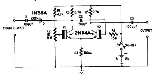
Fig. 702. One-shot multivibrator (uni-vibrator).
A negative input pulse applied to the TRIGGER INPUT terminals reduces the positive potential on the base of transistor V2 and discharges capacitor C2. This reduces the collector current of V2 and lowers the voltage drop across resistor R4. Since the emitter bias of V1 accordingly is lowered, this transistor begins to pass collector current. The transition is rapid, V1 switching on and V2 off and the circuit delivering an output pulse.
Immediately after this switching operation, capacitor C2 begins to discharge and as it does so the positive voltage on the base of V2 begins to rise once more toward the potential of the supply, B. At the end of this discharge interval, V2 again is conducting (on) and V1 nonconducting (off), the quiescent condition of the circuit.
The limiting factor, which sets the length of the discharge time of C2 and therefore the duration of the output pulse, is the voltage drop across R4. Full conduction is not restored to V2 until the base voltage of this transistor equals the emitter voltage; that is, the voltage drop across R4. When V1 is conducting and V2 is cut off, the voltage drop across R4 is governed by the setting of potentiometer R2 (which determines the V1 dc base bias). This variable resistor thus affords a means for setting the duration (width) of the output pulse.
Pulse delay circuit
The circuit in Fig. 703 delivers a negative-going output pulse, the occurrence of which is coincident to or delayed with respect to a negative input-trigger pulse. The delay interval is continuously variable. This circuit employs two rf transistors ( Sylvania 2N94A) , a germanium diode D1 ( Sylvania 1N38A) and a bonded silicon diode D2 (Raytheon I N300) .
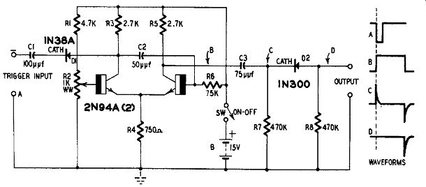
Fig. 703. Pulse delay circuit.
The first part of this circuit is the one-shot multivibrator previously described. Its purpose is to deliver an adjustable-width output pulse (waveform B) in response to a negative input-trigger pulse (waveform A) . The second part is a resistance-capacitance differentiator (C3-R7) which produces sharp, narrow, positive and negative pulses (waveform C) corresponding in time spacing to the rise and fall of the one-shot output pulse (waveform B) . The third part is a series-diode rectifier circuit (D2-R8) the purpose of which is to transmit the negative pulse while blocking the positive pulse of the differentiator output. The negative pulse is selected because the time position (delay) of this pulse may be varied by adjustment of the duration of the one-shot output pulse. The time position of the positive pulse, on the contrary, always coincides with the rise of the one-shot output.
The delay time is varied by adjusting potentiometer R2, the primary function of which is to vary the duration of the output pulse (waveform B) of the one-shot multivibrator section.
It is necessary to employ a modern silicon diode D2 in the rectifier section of the circuit because of the high input and output resistances, R7 and R8 respectively. These high resistance values are necessary to minimize loading of the preceding transistor output circuit. The back resistance of the diode must be very high with respect to the total resistance of R7 and R8. In germanium and early point-contact silicon diodes, the back resistance is so low that rectification ceases when the load resistance is as high as that shown here. The 1N300 diode has a resistance of 10,000 megohms at-10 volts. This rating yields a diode-to-load resistance ratio of better than 10,000 to 1, with respect to R7 + R8.
Simple coincidence circuit In the circuit shown in Fig. 704, the collector supply voltage of the transistor ( Sylvania 2N35) is a rectangular or square pulse having a positive peak amplitude of 6 volts. This pulse voltage is applied to terminals C and D and is furnished by a source having adjustable pulse duration, amplitude, and repetition rate.
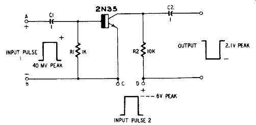
Fig. 704. Simple coincidence circuit.
The circuit may be said normally to have no output in the absence of an input-signal pulse. Actually, the output is never completely zero since a tiny amount of current (due to the ico characteristic of the transistor) flows through the collector circuit when the supply voltage (input pulse 2) is at its peak value. But since the resulting voltage drop across the collector load resistor R2 is so minute (usually of the order of 50 db below maximum voltage output) , the output may be regarded as zero.
When a positive pulse (input pulse 1) is applied to the base of the transistor, through input terminals A and B, at the same time that the collector is positive, the circuit delivers an amplified output signal. If input pulse 2 is zero at the same time that input pulse 1 arrives, the amplifier delivers no output. (Actually, there is a tiny output, regarded as noise, due to R-C leakage through the trans istor) .
Input pulse 2 thus acts to switch on the circuit for transmission and amplification of input pulse 1. The number of input-1 pulses transmitted by the circuit is governed by the width of input pulse 2 which, figuratively, holds open the gate for input-1 pulses. When input pulse 1 is wider than input pulse 2, only that portion of the former is transmitted which occurs during the duration of the latter.
Various desired time-delay actions may be worked out by delaying input pulse 1 with respect to a comparatively wide input pulse 2.
This circuit takes its name from the fact that each output pulse indicates a coincidence between the two input pulses. If the latter are out of step at all times, no output pulses are obtained. When each input pulse occurs at a random rate, the output pulses indicate the number of times they happen to fall into step. The circuit thus serves as the basis for a coincidence counter.
Pulse inverter
Switching-circuit applications sometimes require that a given pulse be reversed in polarity. Depending upon the end use, the operation goes under different names such as inverting, priming, negating, etc.
2N114 /CK762
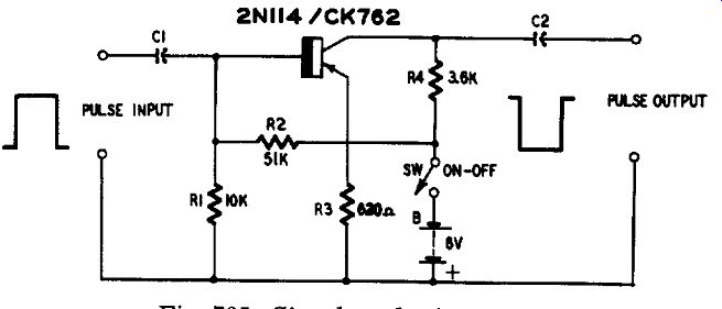
Fig. 705. Simple pulse inverter.
Fig. 705 shows a simple circuit in which inverting occurs as a result of the inherent phase-reversing property of the common-emitter transistor amplifier circuit. Employing a p-n-p type rf transistor (Raytheon 2N114/CK762) for fast rise and fall in the output waveform, the circuit is direct-coupled and is degenerative (unbypassed emitter resistor R3) for improved response. How- ever, isolating capacitors (C1 and C2) will be required in those applications in which the dc biases of the transistor circuit must be protected from short circuit by external circuitry connected to the PULSE-INPUT and PULSE-OUTPUT terminals.