An automatic noise-limiter -- A simple muting circuit for use with FM tuners
In recent years the automatic noise limiter has become an increasingly common addition to high quality FM receivers. Such a circuit greatly simplifies tuning of the receiver by selecting a minimum signal level below which the audio output is muted. Apart from the removal of interstation noise, a squelch circuit can also ensure that only the local transmitters of the national stations are received. With high sensitivity tuners (such as the Nelson Jones design. 1 ), it is not: always immediately apparent when the "wrong" transmitter is being received, until the poorer signal-to-noise-ratio becomes evident. A further bonus is the removal of tuning ambiguities in the absence of AFc,, caused by the shape of the discriminator response curve; a high level, distorted signal is received on either side of the true signal due to the IF falling on the wrong slope of the discriminator response.
The usual method of achieving the a.n.l. function is to detect amplitude modulation of the IF after limiting. If noise is being received, the IF amplitude occasionally drops to zero due to noise cancellation. These gaps in the IF waveform can be detected, and used to operate the muting circuit. However, in a circuit designed to be an add-on unit for existing tuners, it was considered undesirable to make connections into the IF strip of the receiver.
The circuit described requires no modifications to the tuner, except, in the case of monaural reception, removal of the de-emphasis capacitor.
The circuit relies on the fact that, while the signal bandwidth is restricted to a maximum of 53kHz (for stereo signals), the noise bandwidth extends to over 100kHz.
A third order high pass filter is used to reject the signal and yet allow noise to pass through. The resultant signal is amplified and detected, so producing a DC output related to the amount of noise being received. This is used to operate an f.c.t. switch, which mutes the output of the receiver. For mono reception, provision is made for adding a de-emphasis capacitor at the output.

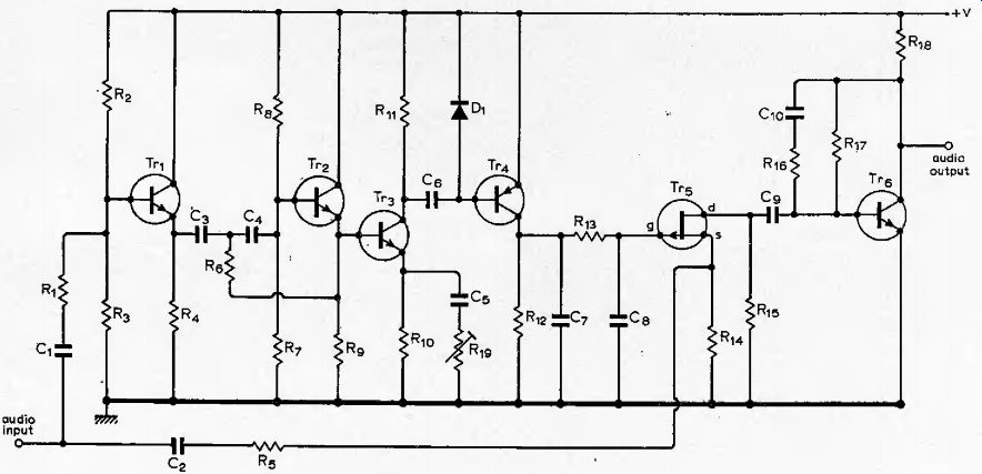
Fig. 1. Complete circuit of automatic noise limiter.

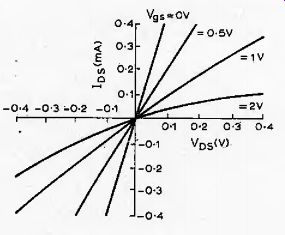
Fig. 2. A sketch graph of the FET
VDS = IDS characteristics.

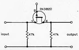
Fig. 3. Elements of the FET switch used to control the receiver output.
--- Components list
Circuit description
The first stage is an emitter follower designed to provide a high input impedance which is substantially constant with frequency. This is important in order to avoid amplitude and phase distortion of the stereo multiplex waveform when fed from a receiver having an appreciable output impedance. The input capacitor to the emitter follower has a value of 68pF, giving a first order high-pass, characteristic with a cut-off frequency of 100kHz. The variation in amplitude at the input when fed from a source impedance of 2.2k-Ohm (as in the Nelson-Jones design) is then only 0.3dB from 1 to 53kHz.
The second stage is a Sallen-Key type second order high pass filter with a cut-off of 100kHz, presenting a low impedance drive to the voltage amplifier stage (Tr3 in Fig. 1.). The detector 3>4 switches when the amplifier output reaches about 1.4 volts peak-to-peak. The detector output passes through a low pass filter (R13, C8) which prevents accidental muting caused by brief noise spikes on an otherwise low noise signal (for example, those caused by badly suppressed car ignition systems). The muting action is performed by a p-channel junction FET used as a switch.
Design of the FET switch
If an FET is operated under conditions of low gate-source voltage and low drain source voltage, it acts as a linear resistance, the value of which is controlled by the gate source voltage (see Fig. 2). For the 2N3820 device used in this design, the minimum "on" resistance is typically around 400 ohm.
In order to avoid distortion it is clear that, in the "on" state, the drain-source signal voltage must be kept to a minimum, as also must the gate-source signal voltage. If either of these is allowed to rise, the drain source resistance will vary over the cycle, and distortion will be generated. Thus an FET, switch as shown in Fig, 3 was found to generate 0.5% distortion at 0,5V RMS input. For higher input levels the distortion increased drastically. This was considered unacceptable for high quality reproduction.
The solution to this is to connect the FET (Tr5) to the virtual earth point of a feedback amplifier, as shown in Fig. 1. At this point, signal levels are very low. In this circuit, distortion was found to be 0.03% at 53kHz, and 0.5V RMS input.
The distortion was almost entirely second harmonic, and at low frequencies the level was reduced still further. The attenuation in the "off' state was found to be ^60db relative to 0.5V RMS.
This design has the added advantage that de-emphasis can be added for mono reception, by connecting a 2.2nF capacitor across the base and collector of the transistor.
Constructional Details
The layout is not particularly critical, but long leads should be avoided, especially to the base of ?>,. It is, of course, important to remember to remove the receiver de-emphasis capacitor if one was fitted for mono reception. In the case of the Nelson-Jones tuner the designer recommends replacing this component with 150pF.
Performance
The circuit has been in use for some time in the author's Nelson-Jones tuner. It has proved to be highly immune to transient interference, and greatly simplifies tuning of the main national and local stations. To enable reception of distant signals a switch has been included to short the gate of Tr5 to ground and defeat the muting operation.
Reference
1. "FM Stereo Tuner" by L. Nelson-Jones, Wireless World, April-May 1971.