Project: Switched Tuned Radio
Tired of playing 'Find the Station'? Six pre-tuned channels make life much easier.
ALTHOUGH A RADIO capable of receiving only a small number of stations might at first appear to be of limited use, for most people it will prove more convenient than a radio having the ordinary, continuous dial tuning scale.
This is due to the fact that people generally only listen to two or three of the stations available to them anyway.
This makes switch-selection of stations an easy and convenient method of obtaining the few of them required to serve the many.
There is nothing new about the idea of push-button tuning, and apart from the use of such tuning in TV sets and FM receivers, this has also featured in a few AM sets over the years. However, whereas FM receivers have tended to use varicap (variable capacitance) diodes in the tuning system, AM designs have used more old-fashioned methods, such as a number of pre-set tuning capacitors. This tends to be more expensive than varicap tuning -- where the set is tuned to the desired frequency by applying the appropriate voltage to the diodes. Here the tuning circuit consists of little more than the switch itself and a few inexpensive preset potentiometers.
Until recently the option of AM varicap tuning was not available, due to the lack of diodes with a wide enough capacitance range. The first of these devices, which appeared several years ago, were not widely adopted as they had a few major drawbacks, the main one being the need for a tuning voltage range of around 1 to 30 V. (This could not be easily obtained from the 6 or 9 volt supply normally employed with portable AM radios.)
The latest vari-caps have been greatly improved and can give a wide enough capacitance swing for an ordinary AM receiver, using a maximum tuning potential of just a few volts.
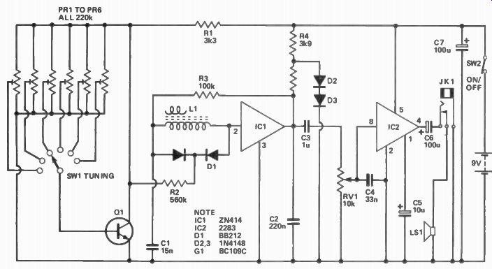
Figure 1. The circuit diagram; Varicap diode, D1, is a dual type.
Varicap Theory
A varicap diode is 'tuned' by applying a reverse bias to the device and, in fact, any semiconductor diode will give the effect! Varicaps differ from ordinary diodes in that the capacitance obtained at a given voltage is guaranteed to be within quite small limits, and they are designed to give good efficiency when used in this manner.
When a diode is reverse biased a 'depletion layer' is formed at the junction of the two pieces of semiconductor material and it is this layer which insulates the pieces of semiconductor from one another, thus preventing a significant current flow.
Since a capacitor is merely two pieces of conductive material separated by an insulating layer (the dielectric), this is what is now formed in the diode. The pieces of semiconductor act as the conductive material and the depletion layer as the dielectric.
The capacitance can be raised and lowered by decreasing or increasing the width of the dielectric. In a varicap the width of the depletion layer varies in sympathy with the applied bias voltage such that a high capacitance value is obtained with a low voltage, and a small capacitance value is produced by a high bias.
Our simple varicap design gives reasonable sensitivity with sufficient volume from the internal loudspeaker and can have up to six switch-selected stations. Covering the full medium waveband, it is completely self contained with an internal ferrite rod aerial and 9V (PP3 size) battery. There is also provision for a crystal earphone and the loudspeaker is automatically muted when the earphone is inserted.
The unit is very easy to construct and does not need any complicated augment.
----------------------
Parts List
RESISTORS (all 1/4 W 5%) PR1 to PR6 220k horizontal preset R1 3k3 R2 560k R3 100k R4 3k9 R5 680R
POTENTIOMETER RV1 10k log with switch ( S W2)
CAPACITORS
C 1 15 nF polyester C2 220 nF polyester C3 1 uF 63 V electrolytic C4 33 nF polyester C5 10 uF 25 V electrolytic C6 100 uF 10 V electrolytic C7 100 uF 10 V electrolytic
SEMICONDUCTORS
Id 1 ZN414 IC2 ULN2283B D1 BB212 D2,3 1N4148 Q1 BC109C
MISCELLANEOUS
SW1 6 way 2 pole rotary switch LS1 40 to 80 ohms min.
speaker JK1 3.5 mm jack socket L1
Medium wave ferrite aerial coil type M WC2
0.1 in. Veroboard
Control knobs Plastic case 140 x 9.5 mm F14 ferrite rod
Mounting clips for aerial PP3 battery and connector to suit Wire, solder, etc.
----------------------
Construction
Cut out a small piece of Veroboard, having 44 holes by 20 strips, then drill two mounting holes for the board plus another two for the aerial. Figure 2 gives full details of the component panel, including the positions of these holes (which are 3.2 mm diameter and accept 6BA fixings.) Next make the required breaks in the copper strips and solder the components and links into place, leaving the semiconductors until last.
Make sure that the electrolytics and semiconductors are fitted on to the board the right way round - it is too easy to connect them incorrectly.
Complete the board by fitting and wiring the aerial. It is mounted in two special plastic clips, fixed to the board using a couple of 1/4 in. 6BA bolts. Only the larger winding of the aerial coil is used, and a quick visual check will show which two tags should be connected to this coil.
We used a plastic case measuring about 150 x 100 x 50 mm for our prototype, which is about the smallest size that will comfortably accommodate the components. The case must be made of a non-metallic material in order that it does not screen the aerial and prevent any signal being picked up.
The general layout can be seen from the photographs and it is advisable to adhere fairly strictly to this. The aerial coil and loudspeaker must be kept a reasonable distance apart or stray feedback between the two could cause a loss of performance or instability. It is also a good idea to have the battery reasonably well separated from the aerial to prevent even partial screening.
The layout must also permit access to the six tuning presets (R1 to R6). The wiring then needed to complete the unit is shown in Figure 2.
The receiver needs L1 positioning correctly on the ferrite rod before the tuning presets are adjusted to their final setting. This is accomplished by first turning RV1 fully clockwise and adjusting SW1 to select PR1 (SW1 fully anticlockwise). L1 is adjusted to bring the set to the low frequency limit of the medium waveband. If a suitable RF signal generator is not available to assist with this, simply make sure that L1 is moved close enough to the end of the rod to permit all the desired stations to be received, without RVI having to be rotated fully anticlockwise. Glue or tape the coil in position once a suitable position on the rod has been found.
It then only remains to adjust each preset to the appropriate station. If you do not require all six tuning positions, leave out the unnecessary pots and wiring to SW1, setting the end stop of the switch to correspond with the number of presets in use. The set has a fairly wide bandwidth and so the tuning is reasonably easy using ordinary miniature presets. Multiturn types or high quality presets are an unnecessary expense in this application.
----------------
How It Works
Basically the unit is a conventional TRF (tuned radio frequency) set covering the standard medium waveband. A TRF is a very simple type of receiver, where the signal from the aerial is amplified and demodulated by a detector stage in order to recover the audio. This is amplified before being fed to a loudspeaker or earpiece.
Sets of this type cannot equal the more sophisticated superhet type in performance but good results are nonetheless obtained. In this design the RF amplifier and detector stages are based on one IC, which has the refinement of an AGC (automatic gain control) giving a consistent volume level from stations of various strengths. The AF amplifier circuit uses a second IC to give a high quality output.
An unusual aspect of the circuit is that it uses switched tuning, accomplished with a varicap (variable capacitance) diode.
This is a semiconductor component which uses a control voltage to alter the value of capacitance in the circuit. It is used in place of a conventional capacitor and is tuned by switched reference voltages to give pre selected stations.

The Circuit
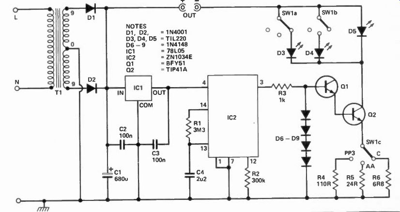
The circuit diagram of the receiver is shown in Figure 1. The heart of the unit is the ZN414 (IC 1). This device contains the RF amp, AGC and detector circuitry thus requiring few discrete components. R3 is used to bias IC1 by way of L1 which is the ferrite aerial. C1 provides a signal path to earth. There are actually two coils on the aerial; the tuned winding and a smaller coupling coil. But as the ZN414 has a high input impedance, it can take the signal direct from the aerial without any impedance matching and the coupling coil is therefore unused in this circuit. R5 is the load resistor for the detector and AGC of IC 1, and C2 is the RF filter capacitor. The ZN414 has no positive supply connection, receiving its positive supply via the load resistor R5. A supply voltage of about 1V3 is needed, obtained from the main 9 V supply using a shunt stabilizer circuit (R4, D2, and D3). C3 couples the audio output signal of IC1 to volume control RV1.
The latter also biases the input of the audio amplifier IC2, a ULN2283B device with a fixed voltage gain of nominally 43 dB -- enough to drive high impedance loudspeaker. C4 provides RF filtering at the input of IC2 and C5 decouples the supply to the input stages of this device. Both these components are needed 70 prevent the audio stages becoming unstable.
D1 is the varicap tuning diode, and is actuality a dual type, the tuning component being formed by the series capacitance of the two sections. With no bias applied, the diodes exhibit a capacitance value of a few hundred picofarads which tune the set to the low frequency end of the medium waveband. With a reverse bias of about 6V, a few tens of picofarads are produced tuning to the high frequency end of the wave band.
Intermediate voltages give intermediate reception frequencies and an appropriate voltage can tune the set to any desired frequency.
Note that the anodes of D1 are biased about 0V8 above the negative supply rail by R3, but in practice this simply means that the tuning voltages are all raised by about 0V8 volts in order to compensate.
The tuning voltages must be stabilized and this is achieved by Q1.
SW1 selects the six tuning potentiometers, and can then be adjusted to give a stabilized potential of between about 0V65 (with the wiper at Q1 collector) and 7V (with the wiper at the other end of the track.) The up per limit is set by the supply voltage available.
-----------------------
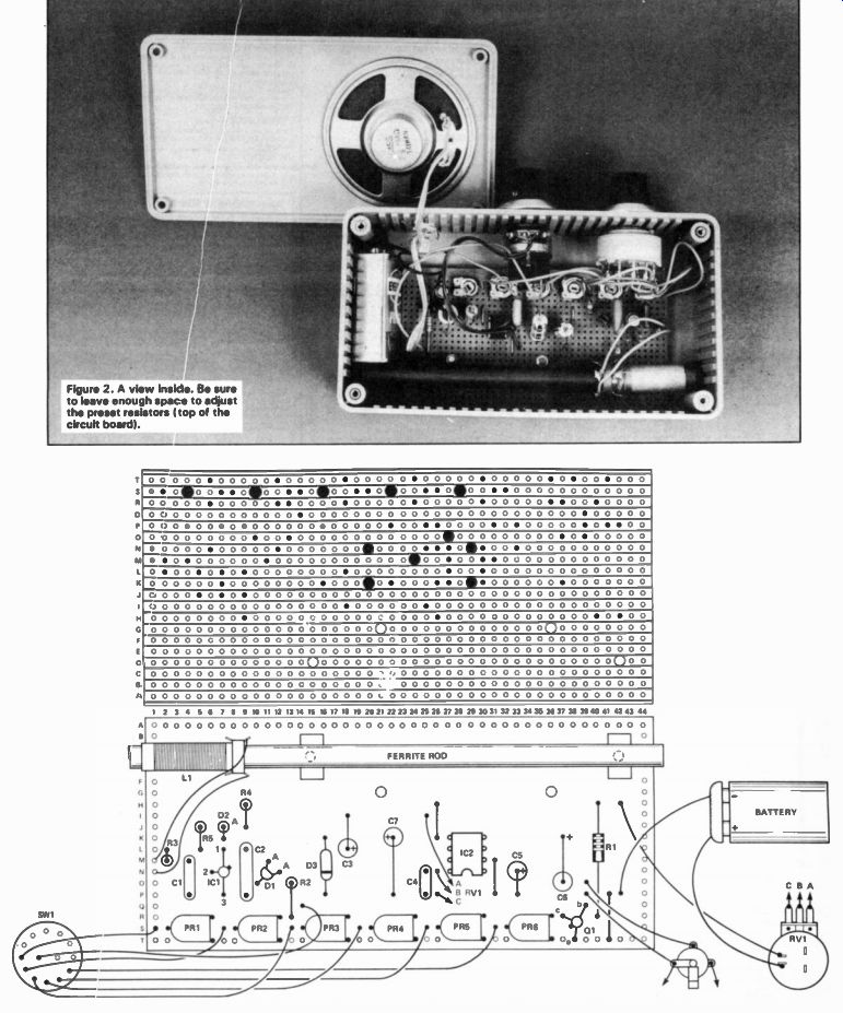
Figure 2. A view inside. Be sure to leave enough space to adjust the preset
resistors (top of the circuit board).
Figure 3 Component layout, with external wiring, and bottom view of the stripboard.
Quick Project: SIMPLE TIMER
THIS VERY SIMPLE timer unit turns on an LED between two and five minutes after switch on. The time delay is continuously variable within these limits. To start a new timing run the unit is simply switched off, then on.
At switch-on, Q1 will be cut off because C1 is uncharged and will take Q1's gate to the negative supply potential.
Therefore, Q2 receives no base current and is also cut off.
C1 will charge from the supply line by way of RV1, R1; the rate of charge can be varied by means of RV1 . After a time the charge on C1 will be sufficient to bias Q1 and D1 into conduction: D1 is used to raise the gate threshold voltage of Q1 so that fairly long time delays can be obtained using practical resistance and capacitance values. A VMOS device is used for Q1 as they draw insignificant input current and there is, therefore, no significant leakage of the charging current.
When Q1 starts to switch on, Q2 also starts to conduct and passes additional charge current to C1, via D3. This results in both Q1 and Q2 rapidly switching hard on and D2 lights up due to the current flow through Q2, R4, D2, and D1 . The regenerative action of Q3 ensures that D2 switches on cleanly and rapidly. When SW1 is switched to the 'off' position, it discharges C1 so that a new timing run can commence.
C1 must be a low-leakage electrolytic or tantalum type, otherwise leakage through it will greatly extend the delay time and could pre vent Q2 from switching on at all Q1 can be any N-channel VMOS device (VN66AF, VN67AF, etc).
Project: INTELLIGENT NI-CAD CHARGER
It does the thinking for you The advantage of using NiCad batteries in equipment such as flashguns, electric models and cassette recorders is that they are considerably less expensive, in the medium to long term, than ordinary (non-rechargeable) batteries. One drawback, however, is the bother of keeping track of how long they have been on charge. Most NiCad manufacturers claim that overcharging cells does not do them any harm, so that it does not matter if they are left too long on charge. The real problem tends to be that the cells are not left on charge long enough, so that they fail prematurely. Another problem is that, in order to achieve their full lifespan, NiCad cells should go through full charge discharge cycles, since partial charging can reduce operating life.
What is needed is a charger that knows when to switch itself off - but does not cost a fortune. The Intelligent NiCad Charger fits these requirements precisely. It has a built-in timer which cuts off the output approximately 15 hours after switch-on (normally NiCads require 14 to 16 hours to fully recharge) and uses a simple circuit that requires few components.
NiCad cells must be charged from a source which limits the charge current to a safe level as they are likely to be damaged if this current is exceeded.
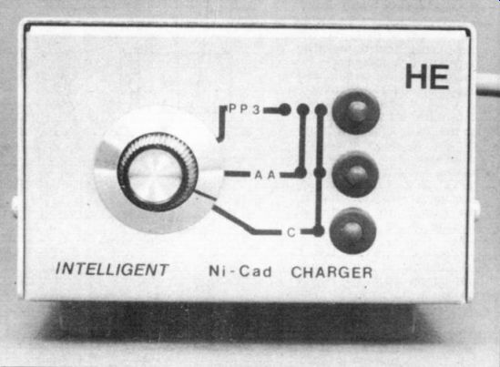
This charger uses a constant current source that gives switched, nominal output currents of 11 mA, 50 mA, and 180 mA. These currents are suitable for PP3, AA (HP7), and C (HP11) size NiCad cells respectively. The unit can charge at one time, either one PP3 size battery or up to six AA cells, or up to four C size cells.
Timer
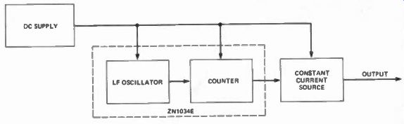
The normal choice these days, for practically any timing application, is the 555 IC; but not in this case. The Old Faithful is unsuitable here because of the impractically high component values (such as a 54 megohm resistor and a 1000 microfarad capacitor!) required to give a timing run of 15 hours. While this is quite feasible in theory, in practice the leakage current though the capacitor would be such that the timing pulse would, almost certainly, never end! An alternative form of timer is one that uses a counter circuit fed by an oscillator.
The output pulse usually lasts for a certain number of oscillator cycles.
The ZN1034E, the device used in this circuit, is a counter-timer IC of this type.
It requires 4095 (internally generated) oscillator pulses before the counter changes state, and this enables quite long output times to be obtained using fairly low RC timing component values.
In fact, the output time of around 15 hours is obtained even without having to use an electrolytic capacitor in the timing circuit.
In Use
AA or 'C'-sized cells must be fitted into a plastic battery holder which has a PP3 type connector to fit directly onto the output connector of the charger. The cells must be connected in series and the plastic holders ensure this, but be sure to fit the batteries into the holder with the correct polarity! Of course, a PP3 NiCad simply connects directly with the output connector. Remember to set SW1 for the appropriate charge current before connecting the cells. Due to the tolerances of the components, it is possible that the charge time might be somewhat outside the required 14 to 16 hour range. If necessary, the value of R1 can be raised or reduced and this will give a degree of control over the charge time. However, if the error is only small, it is probably not worthwhile bothering with.
-----------
How It Works
The charger is powered from the AC mains supply and gives a DC output suitable to charge NiCad batteries. It is essential that NiCad batteries are charged at a low current or they may become damaged; the output is therefore supplied by a constant current source, which sets the charge current at a safe level.
A counter circuit is used to control the charge time and at switch-on it enables the current source to function normally. After the counter has received 4095 pulses from the oscillator (which takes around 15 hours) the counter output changes state so that the current source is switched off and the battery no longer receives any charge current.
The mains supply is converted to a smoothed, low voltage DC supply by means of conventional full wave power supply circuit, T1, D1, D2 and C1. No on/off switch is used as, presumably, the unit will be unplugged when not in use.
IC2 is a precision timer device which contains an oscillator, 12-stage binary counter, and control logic circuitry. It requires a stabilized 5 volt supply and has an internal 5 volt shunt regulator, but this can easily be damaged by excessive current so an external 5 volt monolithic voltage regulator (IC1) has, therefore, been used. C2 and C3 are supply decoupling capacitors which prevent IC1 from becoming unstable.
Pin 1 of IC2 is the trigger input and, as it is taken low by being connected to the negative supply rail, IC2 is triggered as soon as the unit is connected to the mains supply. At the same time, the Q output at pin 3 goes high, to approximately + 5 volts. The time for which the Q output stays high is determined by calibration resistor, R2, and timing components R1 and C4. With R2 at the specified value, the timing components give nominal output pulse length of 7500 RC, that is, 54450 seconds 115 hours and 7 1/2 minutes/. R3 plus D6 to D9 form a simple shunt regulator circuit that gives potential of about 2.4 volts at the junction of R3 and D6. D6 to D9 are ordinary silicon diodes, forward biased and give a voltage drop of about 0.6 volts across each (4 x 0.6 volts = 2.4 volts). This voltage is used to drive Q1 and Q2 which are connected in the Darlington configuration and form the basis of the constant current generator circuit.
There is a drop of about 1.2 volts from the base of Q1 to the emitter of Q2, leaving 1.2 volts across whichever emitter resistor is selected by SW1.
This gives an emitter current of roughly 11 mA with R4 in circuit, 50 mA with R5, and 180 mA with R6.
These are the appropriate charge currents for PP3, AA, and C sized NiCad batteries respectively and provided a suitably low resistance path is present in the collector circuit, the collector current will be virtually equal to the emitter current. By connecting the NiCad cells in the collector circuit of Q1/2, therefore, these cells can be charged at the appropriate current.
The charge current always passes through LED indicator D5 and this shows whether or not the battery is properly connected to the unit and is charging. It also shows that the charge period has ended since, after 15 hours approximately, the Q output of IC2 goes low, switching off Q1 and Q2 and cutting off the charge current. With SW1 in the "AA" position, Q4 is switched in parallel with Q5 and in the "C" position both D3 and D4 are switched in. There are two reasons for doing this; one is simply that the LED display makes it very clear which charge current the unit is switched to (one LED for the PP3 mode, two for the AA mode, and three for the C model so that there is little risk of charging a cell at the wrong rate. It also keeps the current through the LED indicators to an acceptable, though high, level when the unit is used at the highest charge current. A secondary role of the indicator diodes is to prevent the NiCad cells discharging through the charger.
--------------------
Construction
The prototype was built in to an inexpensive aluminum case measuring 133 x 102 x 64mm, but any metal case of similar dimensions should do. SW1 is mounted on the left side of the front panel, with D3, D4 and D5 fitted in panel holders on the right. Use large (0.2in.) LEDs and also three LEDs of exactly the same type (not different colors) or, due to differing LED voltages, one or two of the indicators may not work. The design is a little unusual in that it allows the LEDs to draw so much current - 60 mA each, in the 'C' position - however, no problems arose during repeated tests in our workshop. - Ed.
1. A solder tag should be fitted to one mounting of Ti in order to provide a chassis connection point for the mains earth lead. Be sure to use a three-core mains lead and earth the case securely.
Drill two holes in the rear panel, one for the output lead and one for the mains cable, and fit them with grommets to protect the cables.
The output connector is an ordinary PP3 battery connector - remember to thread the leads through the hole in the rear panel before soldering them in place! Finally, connect the mains lead, and give the wiring a thorough check before switching on.
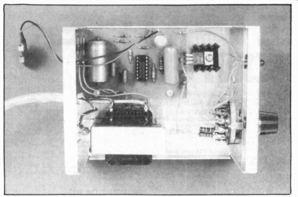
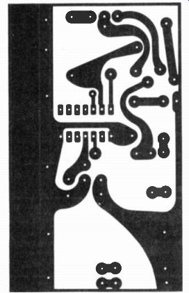
Figure 1. PCB foil pattern of the Intelligent Charger.
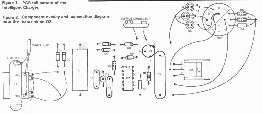
Figure 2. Component overlay and connection diagram: note the heatsink
on Q2.
Parts List
Resistors (all 1/2 watt 5%) R1 3M3 R2 300k R3 1k R4 110R R5 24R R6 6R8
Capacitors
C1 680u F 25V electrolytic C2, 3 100nF polyester (C280 series)
C4 2u2 polyester (C280 series)
Semiconductors
IC1 78L05 (5V, 100 mA) regulator
IC2 ZN1034E
Q1 BFY51
Q2 TIP41A D1,2 1N4001
Q3,4,5 TIL220 (0.2 in. red LED)
D6,7,8,9 1N4148
Miscellaneous
SW1 3 way, 4-pole rotary T1
Standard; 9-0-9 volt, 500 mA secondaries PP3 connector, case. PCB control knob, panel holders for LEDs, finned heatsink for 02, mains lead, wire, solder, etc.
Buylines
There should be no problems in obtaining the components for this project. Total cost, including case and heatsink, should be about $20 (1982, USD).
Project: INTRUDER CONFUSER
The simplest security system imaginable.
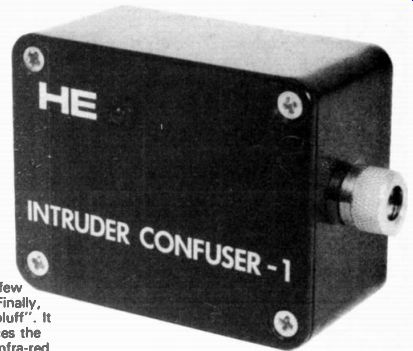
THIS OSTENTATIOUS DEVICE is intended to puzzle a would-be intruder or other unwanted visitor, and make him decide that it is safer, after all, to leave your premises untouched and try elsewhere.
All it does, actually, is to flash the LED steadily, day and night, and pretend to be something complicated, such as an infra-red beam projector. The case has a dummy barrel on the outside through which infra-red rays might be seen emerging, if you could see infra-red rays. On the other side of the room you can place a reflector, as if deflecting the beam to a receiver. The purpose of the flashing LED is to attract attention to the device. Simple, innit? Dead cunning! Preferably, it is placed just inside a window so that it can be seen by the intruder before he tries to break in. This device is akin in spirit to those objects, seen in department stores, that look like flying saucers and could by TV cameras scanning the shoppers, but probably are not. Like the Confuser, they are an effective deterrent, yet cost much less than the real thing.
In some ways the Confuser is better than a real alarm system. For one thing it doesn't give false alarms (nobody pays the slightest attention to them anyway). On the other hand a few Confusers around the place will suggest that an alarm system really is in action, or if you have genuine system you can advertise the fact by installing a few Confusers as window dressing. Finally, there is the deadly "wild goose bluff". It works like this: The burglar notices the Confuser, thinks it might be an infra-red system, steps carefully over the imagined beam -- straight on to a carefully positioned pressure-mat!
Construction
The circuit is assembled on a piece of strip-board as shown in Figure 2 and mounted inside a small case. It is advisable to purchase a case for this project rather than use the legendary tobacco-tin; a professional appearance makes the deception more likely to succeed. Building the circuit presents no problems. The leads of the LED are bent and it is mounted to protrude through the hole in the lid. If the LED doesn't light you have probably soldered it the wrong way round! Apart from this, the circuit should work immediately the battery is connected. The simplest way of making contact to the cell is by solder-tags; these are held against the terminals by a wide rubber band while the battery itself is held by a 'sticky fixer' or 'Blu-tak'.
The device should look as if it projects infra-red rays - or perhaps some hitherto unknown type of radiation! The barrel used for the prototype was the casing of a coaxial plug and it looked suitably imposing, but any suitable scrap item that is to hand will do the trick.
The Confuser should be positioned so that it is "beaming" rays across a region of the room. Do not, for example, place it on the sill pointing at a potted plant! Also, it should be placed so that it could have wires leading to it, wires which are, of course, invisible from outside.
How It Works
The circuit is extremely simple, using only 3 components. It is based on the LM3909 LED flasher, a versatile low cost integrated circuit. When connected as shown in Figure 1, the LED emits a bright flash of light about once a second. The "C"-sized dry cell lasts at least 7 months, running continuously. There is little point in fitting a switch. The device is quick to build and costs little, making it feasible to have three or four to be set at strategic points about the house
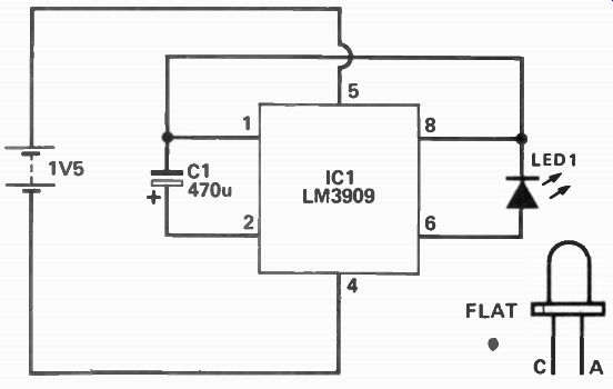
Figure 1. Circuit diagram of the Intruder Confuser.
Parts List
SEMICONDUCTORS
IC1 LM3909
LED flasher
LED1 0.2" LED, any colour but red is the most 'threatening'
CAPICATORS C1 470u, 10V electrolytic
MISCELLANEOUS
0.1" matrix board, 24 strip x 22 hole
LED panel clip 2 x terminal pins
Case, 62mm x 78mm x 37mm
Rubber band and 'Blu-Tak' Wire, solder
Coax plug or round scrap object 2 x solder tags 1 x C-size battery
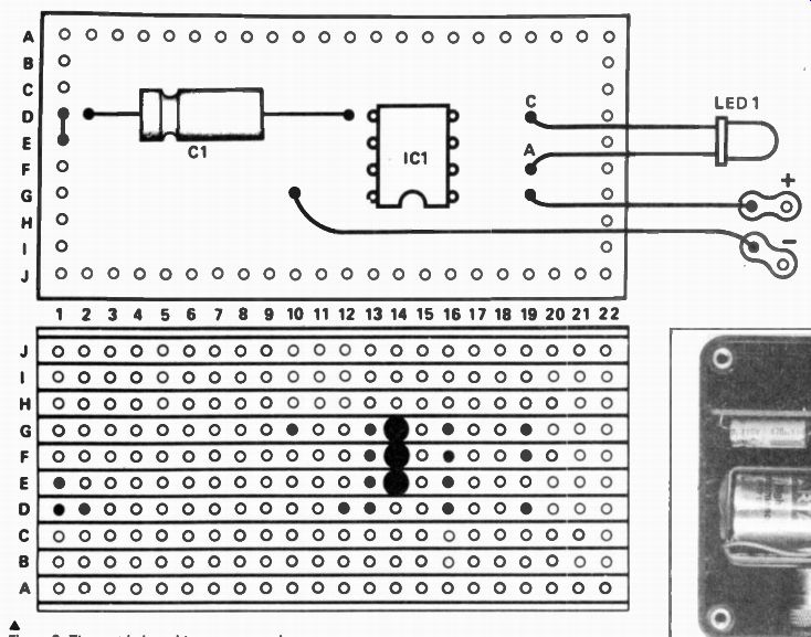
Figure 2. The matrix-board layout, top and bottom views.
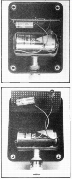
Figure 3. The internal workings - not a lot of it!
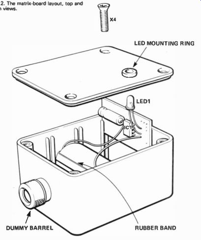
Figure 4. The rubber band is NOT the power source!
-----------------
(adapted from: Hobby Electronics magazine)
Also see:
SCALING the Hi-Fi HEIGHTS (Part 1)