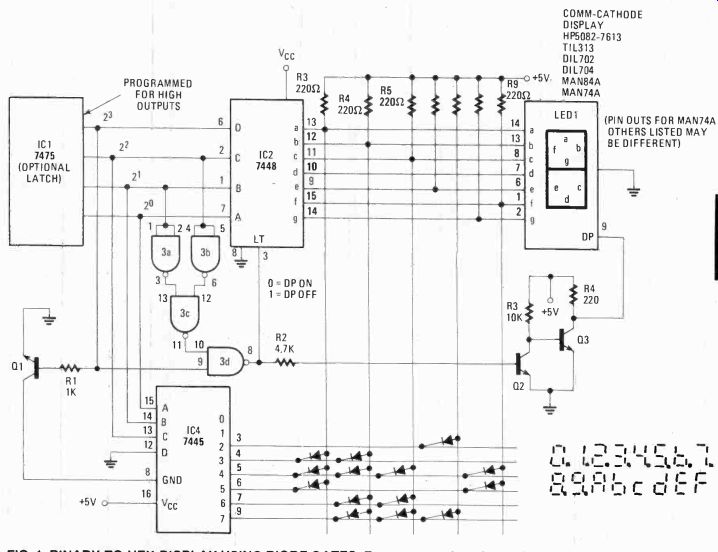
FIG. 1. BINARY-TO-HEX-DISPLAY USING DIODE GATES. For some readers, it may
be necessary to reread the text to understand the unusual functions of the
quad-section NAND IC3 and BCB-to-decimal decoder/driver IC4. If you want
to figure it out yourself, start at IC3-d whose output should be at a low
state when the hex count is A through F inclusive. When output pin 8 of
IC3-d is low, Q2 drives Q3 to conduct, bringing pin 9 of LED1 to ground-turning
off DP (decimal point) in LED1.

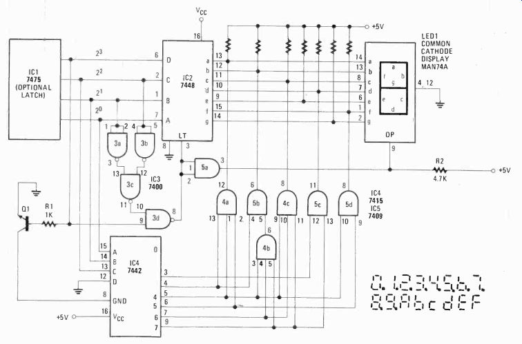
FIG. 2. BINARY-TO-HEX DISPLAY USING COLLECTOR GATES.
Same results as Fig. 1 with IC4 and IC5 replacing the diode gates.
IC5-a, a quad 2-input positive AND gate with open-collector output, takes the high signal to LT (pin 5) of IC2 as an input, and drops all of the 5-volts DC across R2, effectively turning off the DP (decimal point) in LED1.
What may be junk to many represents a wealth of theory and a practical hex display D.E. PATRICK USING INEXPENSIVE SEVEN-SEGMENT DISPLAY LED'S AND SOME logic (mental and TTL) you can make sense out of a microprocessor's front panel, ease debugging procedures, or provide an alternative to some expensive monolithic binary to hexadecimal (hex) displays. All this can be accomplished for only a few dollars. Even less, if you own the LED displays.
The TTL circuits presented are recommended only if you have the parts in your junk box.
From the junk box-only
The circuits in Figs. 1 and 2 may be primitive, but they might represent your cheapest out, if you have an abundance of TTL junk. Operation is similar, with one using diode gates, while the other uses open-collector AND gates.
In either case, to prevent any user-perception errors in reading the LED's, the right-hand decimal point (DP) is lit for all numerals 0 thru 9, while during hex alpha A-B-C-D-E-F readout, represented as A-b-c-d-E-F, the decimal point is out. The DP is used in this display configuration to eliminate any confusion, which might otherwise take place, between the numbers 6 and hex alpha b-they would be identical otherwise.
An optional 7475 latch, IC1, allows the use of active low or high input signals by programming its Q and Q outputs. At the same time, it provides the ability to latch input signals.
But, when deleted, active high-input signals are required.
For active binary high-input signals to IC2, a 7448 BCD-to-seven-segment decoder driver, with active high outputs, decimal 0 through 9 or binary 0000 through 1001 are displayed normally. The DP is also lit via IC3 for all numerals.
When the input of IC2 exceeds decimal 9 or binary 1001, the lamp test (LT) input to IC2 is activated by being brought low via IC3, extinguishing the DP and forcing the outputs of IC2 to an active high state. If nothing else happened for hex inputs of A through F there would appear a numeral "8" or LED1 with the DP extinguished-read on.
Looking at the operation of IC3, the NAND gates IC3-a and IC3-b are inputted with B and C inputs of IC2 which represents 2' and 22, respectively. See Fig. 1 or 2. Both IC3-a and IC3-b receive low inputs at the same time when, 8 and 9 binary numerals are received with both outputs going high, and inputting to IC3-c. This results in a low signal supplied to IC3-d, pin 10, which will have a high output no matter what the input on pin 9 of IC3-d might be. It just so happens that pin 9 is driven high by bus D (23 signal to pin 6 of IC2), but the output of IC3-d remains high as stated before. When A through F are hex outputs from I C1, and D bus (23) is always high, and the paired B and C buses are never both high at the same time. Thus the output of IC3-d is always high for alpha characters, and those coincide with the high D bus to drive IC3-d to a low, or ground. Under these conditions, the light test (LT, pin 3 on LC2) goes low, turns off the DP, and lights up all segments (a through g of LED 1) displaying an "8" as mentioned earlier.
Ground is applied to IC4 a 7445 BCD to decimal decoder driver in Fig. 1 or a 7442 decoder in Fig. 2, with active low outputs. When D goes high on IC2, Q1 conducts and drives pin 4 on IC4 to ground. IC4 decodes the three Least Significant Bits (LSB's), A, B, and C, while its D input is tied to ground. But, the decimal 0 and 1 outputs are not used, so albeit ground is applied when D goes high (a decimal number 8) IC4 effectively performs no operation for 1000 or 1001 binary inputs. The outputs of IC4 feed a series of diode gates in Fig. 1 and open collector AND gates in Fig. 2. In either case, the gates act to turn off unwanted segments in the display to form the necessary alpha characters.
For example, consider a 1010 binary input, or hex A. IC4 sees only the LSB's 010 or a decimal 2. The decimal 2 is outputted from IC4 as a active low signal and turns off the d segment of LED1 in Figs. 1 and 2. Thus the character A is formed, with segments e-f-a-b-c-g still remaining lit. Next, consider a binary 1011 input. IC4 sees only the LSB's 011 or a decimal 3. The decimal 3 is outputted and turns off the a and b segments; thus, the character b is formed. And the remaining characters c-d-E-F are formed in like manner.
The 220-ohm pull-up resistors R3-R9 used across the output lines of the 7448 driver has the net effect of controlling brightness, and the lower the value of those pull-up resistors, the brighter the display, but do not exceed the limitations of the LED devices used.
Finally, a large number of TTL or equivalent gate combos and/or logic families might be used to accomplish the same end. Unless you have the parts shown on hand, it would hardly be worth while purchasing them new. Admittedly, using the parts discussed in this article is similar to a trip down TTL memory lane. Nevertheless, you'll be pleasantly surprised by the dollar savings--an experience that should happen every day.