AMAZON multi-meters discounts AMAZON oscilloscope discounts
Voltages can usually pinpoint the trouble to one particular part of the circuit, provided they are read carefully and their meanings interpreted properly. This can save still more time, because the technician can often go directly from the voltage readings to the defective part or conductor.
Some defects affect only one voltage in a stage, whereas others cause more than one to be wrong. Some defects will cause a loss of collector current, but others can cause it to be much higher than normal. The base-to-emitter voltage, or bias, will go to zero in some cases, or it may reverse in polarity.
Other troubles cause the bias to increase until it is higher than normal, but at the same time cause a loss of collector current flow instead of the expected increase. All these conditions mean something to the alert technician, leading him directly to the trouble area in a minimum of time.
Naturally the voltage change for each defect will depend on the type of circuit and the value of the components. However, if the popular common-emitter types of amplifier and oscillator circuits shown previously are studied, the basic principles can be learned and applied to almost any transistor circuit en countered. Troubles will be placed in the circuits and the voltages noted for each type of trouble. The drawings and charts in this section will serve as a handy reference when a radio with defective voltages is encountered in the shop. Later, after enough experience has been gained in measuring and analyzing transistor voltages, this will also become routine.
CAUSES OF VOLTAGE ERRORS
The first part of this section will show various voltage errors and the troubles which can cause them to be that way. The second part will discuss various components and show what happens to the signal and the voltages when each component becomes defective.
We will always assume the battery voltage and current have already been checked, so no trouble can exist from a defective battery. Voltages are read by a meter with a resistance of 20,000 ohms per volt or higher, and the radio is tuned off the station frequencies to prevent signals from entering it.
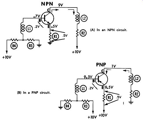
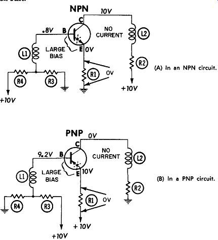
Fig. 6-1. Normal DC voltages.
Before any defects occur, we'll assume the voltages in the NPN circuit (Fig. 6-1A) and the PNP circuit (Fig. 6-1B) read as shown.
Wrong Base Voltage
Very few defects will cause the base voltage to be far from normal when measured with respect to ground, except those in the base circuit itself. The reason is that the base voltage is usually obtained from a voltage divider; and unless the base is disconnected from this divider, or the divider itself is defective, the base voltage cannot change by a very large amount.
Small variations in base voltage do not usually cause the circuit to be inoperative, provided the base-to-emitter current is normal.
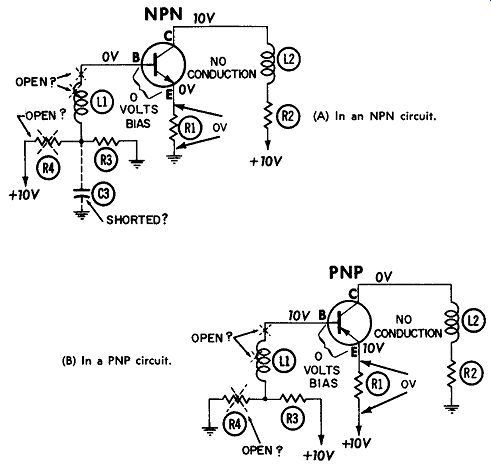
(A) In an NPN circuit. (B) In a PNP circuit.
Fig. 6-2. Open base circuit.
In Fig. 6-2A the NPN transistor has lost its base voltage, and also its bias between base and emitter. When the base voltage is lost in an NPN transistor, the transistor no longer conducts.
Current ceases to flow through emitter resistor R1; so there is no longer any voltage drop across R1. Current through L2 and R2 will also stop flowing, causing the collector voltage to read the same as the positive supply voltage fed to that stage.
In other words, a loss of base voltage in an NPN circuit causes loss of conduction, which can also affect the emitter and collector voltages. Possible defects which can cause these conditions are an open conductor in the base circuit, open coil L1, open base resistor R4, or shorted capacitor C3.
If the base lead should open in the PNP circuit in Fig. 6-2B, the base voltage will go more positive instead of negative. The reason is that the emitter has 10 volts on it and the resistance inside the transistor is very small between the base and emitter.
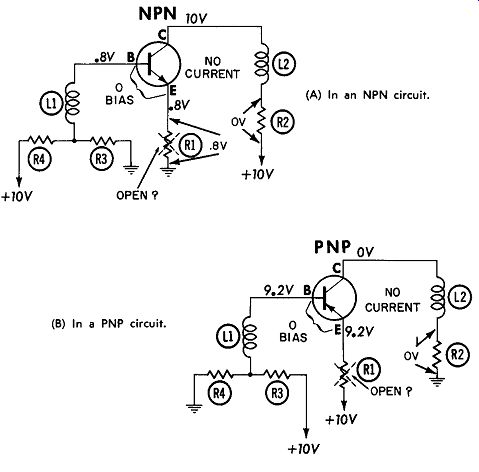
(A) In an NPN circuit. (B) In a PNP circuit.
Fig. 6-3. Open emitter circuit.
The base, therefore, goes to the emitter voltage when it loses connection with its own voltage divider R3-R4. The base "assumes" the emitter instead of collector voltage because the internal resistance between base and collector is quite high.
The loss of base-to-emitter bias voltage in Fig. 6-2B causes the current through R1, R2, and L2 to stop. The voltage drop across the resistors therefore disappears, causing the emitter to go to 10 volts and the collector to zero or ground. This set of conditions is due to the open base conductor, open transformer L1, or open voltage-divider resistor R4. The base voltage to ground may not actually read the full 10 volts as shown because of the voltmeter resistance, but it will not be normal.
The lack of conduction, the loss of bias, and the wrong base voltage point to trouble in the base circuit.
Loss of Base-to-Emitter Bias
The loss of normal voltage between base and emitter can be due to another defect-namely, an open in the emitter circuit. This is shown in Fig. 6-3, where emitter resistor R1 or one of its connections has opened. The results are very similar to the open base circuit, except the base voltage now is nearer normal when measured with respect to ground.
In the NPN circuit (Fig. 6-3A) the base voltage remains very close to normal, rising only slightly because the base current has stopped flowing. The floating emitter now takes on, or assumes, the neighboring base voltage of about 0.8 volt. Again this is due to the very low internal resistance between base and emitter, which tends to keep the voltages very close together on those two elements. Actually, when placed between base and emitter to measure the bias, the voltmeter will read zero or very slightly negative on the base with respect to the emitter. Normally, of course, it is slightly positive.
The transistor cannot possibly conduct while the emitter circuits are open, so no voltage is dropped across collector coil L2 or collector resistor R2. By looking at emitter voltage only, one might assume the transistor is conducting. But here the floating emitter is getting its voltage from the base. This is why it is important to read all voltages on a transistor, including its bias, before making any conclusions about the stage.
In the PNP circuit (Fig. 6-3B) the emitter resistor has also opened. As might be expected, the floating emitter element takes on the neighboring base voltage through the low internal resistance in the base-emitter diode. The base voltage to ground stays fairly close to normal, since the base is still attached to its voltage-divider resistors R3 and R4. There may be a slight variation in base voltage because no base current is flowing, but it would appear to be well within normal limits to the troubleshooter. The emitter voltage to ground might also be considered within normal limits. But when the meter is placed between the base and emitter, the bias will read zero or slightly reversed from normal. Collector voltage to ground reads zero because there is no collector current; therefore, no voltage is produced across L2 or R2.
An open emitter resistor is a quite common defect in power output stages, where the resistor also serves as a fuse for the transistor.
Remember, when checking the resistance of a resistor or coil in a transistor circuit, that the ohmmeter has an internal battery which will affect the resistance of the transistor diodes.
The latter resistance will therefore shunt the resistance being measured. However, whenever a transistor is reverse-biased, its resistance becomes very high. So, when the resistance of the coil or resistor is measured, and the ohmmeter leads are then reversed and the resistance measured again, the resistance reading probably will change. The higher reading will be the one least affected by the transistor. It is therefore the more accurate one.
Loss of Emitter-to-Collector Voltage
The loss of voltage between the emitter and collector leads is very easy to spot because all elements appear to have about the same voltage on them. This condition is shown in Fig. 6-4, where the collector circuit has opened.
In the NPN circuit (Fig. 6-4A) with an open collector lead, the collector voltage drops to a very low value. This acts like a vacuum-tube circuit with an open plate lead, where the plate voltage drops to zero. In the transistor circuit, however, the collector voltage may not drop all the way to ground because
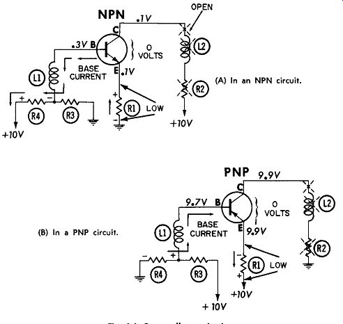
(A) In an NPN circuit. (B) In a PNP circuit.
Fig. 6-4. Open collector circuit.
the emitter may still have a slight voltage on it. Collector current, of course, stops flowing. But because electrons cannot flow into the collector circuit, more of them flow into the base circuit and cause an increase in base current. This base current flows through emitter resistor R1, and may now cause a read able voltage drop across R1-in this instance, 0.1 volt.
What happens next is quite interesting. As the collector voltage drops below the base voltage, the transistor becomes a low resistance between base and collector. (The collector diode is now forward biased.) The base-to-emitter diode already had a low resistance; so now the resistance across the whole transistor, from emitter to collector, becomes very low. The collector will take on, or assume, whatever voltage is on the emitter, leaving no difference between those two elements. This condition could be caused by open collector transformer L2, open collector resistor R2, or an open connection in the collector circuit.
(A) In an NPN circuit. (B) In a PNP circuit.
Fig. 6-5. Open emitter lead within the transistor.
The PNP circuit in Fig. 6-4B has a similar defect, causing all voltages to read almost the same in that stage. However, since the positive side of the battery is connected to the emitter through R1, all voltages go in a positive instead of negative direction.
The emitter voltage goes up slightly because less voltage is dropped across R1, and the base voltage does likewise because the base current increases (see the arrows). The collector voltage assumes the emitter voltage because of the low internal resistance between the emitter and collector elements. Thus, there is no voltage difference between emitter and collector, making this a very easy trouble to spot.
Open Lead Inside the Transistor
So far we have learned what happens to voltages when either the base, emitter, or collector circuits are opened, either by a defective part or by a broken conductor. A different set of voltages will be read, however, if one of the leads inside the transistor should open.
In Fig. 6-5 the emitter lead has opened in the transistor.
The effect of this on the NPN transistor circuit (Fig. 6-5A) will be studied first. The flow of current through the transistor stops because the transistor has become an open circuit. Since the voltage at the emitter was produced by the normal current flow through emitter resistor R1, the emitter voltage will now drop to zero. Also, since collector current stopped flowing through L2 and R2 in the collector circuit, there will be no voltage drop across them. Collector voltage rises to the full battery voltage of 10 volts. The base voltage is not affected much because it is still connected to its voltage divider R3-R4.
This causes a very odd-looking situation; namely, the transistor has a very high forward bias (0.8 volt) between base and emitter, but shows no sign of drawing any collector current.
This is very unusual, indeed, because we would normally expect the transistor to conduct very well with such a large bias.
This leads us to suspect an open lead within the transistor.
The PNP circuit (Fig. 6-SB) demonstrates a similar defect.
The base voltage remains very close to normal because it is still connected to its voltage divider R3-R4. When the transistor is open, however, collector current does not flow; so the voltage drops that were present across the emitter and collector resistors disappear. This puts the emitter at the same potential as the supply voltage, or 10 volts. The collector, grounded through L2 and R2, goes to ground or zero volts.
The important point is that the forward bias measured between base and emitter is unusually good (0.8 volt); yet the transistor does not conduct. The reason, of course, is that a lead is open inside the transistor.
The emitter lead is not necessarily the only one that can open, although it seems to do so more than the others. If the base lead opens internally, the indications will be the same as seen for the emitter. If the collector lead opens, conduction is low, bias is normal, and the collector voltage goes to its source potential.
Review of Open Circuits
We have shown what happens to voltages when a lead opens in either the external circuit or the transistor itself. Now let's review these interesting situations.
Fig. 6-6 shows a summary of the most important voltage changes that took place with each defect. These changes will tip the troubleshooter off to the part of the circuit where the trouble probably lies.
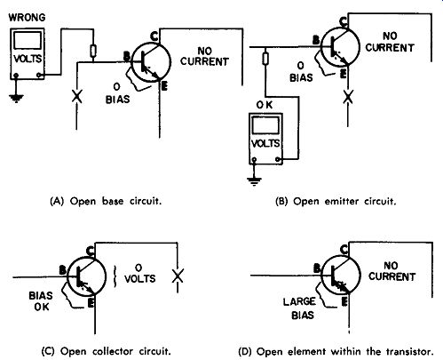
(A) Open base circuit. (B) Open emitter circuit. (C) Open collector circuit.
(D) Open element within the transistor.
Fig. 6-6. Results of open conditions in a transistor circuit.
When the base circuit opened (Fig. 6-6A), the base element lost its connection to the voltage divider. This caused an error in the base voltage when measured ·to ground. Also, since the internal resistance between base and emitter is relatively low inside the transistor, the floating base element goes very close to the emitter voltage. This will show up when the voltages between elements are measured using the emitter as a reference. The base-to-emitter voltage will read zero. With no bias, the transistor cannot conduct, which will affect the emitter and collector voltages. There will be no voltage drops across the emitter and collector resistors.
The open emitter circuit (Fig. 6-6B) caused a similar set of conditions, except the base voltage to ground was fairly normal. The floating emitter lead, however, takes on the base voltage because of the low internal resistance inside the transistor. This causes the bias, when measured between base and emitter, to read zero, or even slightly reversed from normal in some instances. (The meter may actually go slightly below zero when it should be reading upscale.) This condition also causes the collector current to stop flowing.
The open collector circuit (Fig. 6-6C) caused the biggest change in collector voltage. In fact, the collector voltage changed so drastically that the internal resistance of the collector diode (collector-to-base) became very low. This caused a very low resistance all the way through the transistor, and the collector and emitter both went to the same voltage. When the collector voltage is measured with respect to the emitter voltage, this will show up as a zero difference. Such a condition is easy to spot because it is so far from normal. Usually, the collector-to-emitter voltage is the largest one between any two leads of the transistor. Another condition which will cause the emitter and collector to have the same voltage is a shorted transistor. This is a common trouble in power transistor output stages. It will be discussed in a later section.
The open lead inside the transistor (Fig. 6-6D) caused a larger-than-normal voltage between base and emitter, but a complete loss of collector current. These two conditions show that something is wrong, because a large bias should normally produce plenty of current. The lack of collector current will be evident by the lack of a voltage drop across the emitter and collector resistors.
Several rules might be made from these observations:
1. If there is a loss of conduction, zero bias, and wrong base voltage, trouble is in the base circuit.
2. If there is "0" bias with normal base voltage, check for open emitter resistor (CAUTION: In many oscillator or converter circuits, it is normal for the bias to be zero or reversed).
3. If there is no difference between the collector and emitter voltages, the trouble may be an open in the collector circuit ( or a complete short between emitter and collector; this usually happens to high-power transistors).
4. If a transistor has a better-than-normal bias voltage but no conduction, check for an open within the transistor.
Most of these defects had one thing in common-they produced a decrease in collector current. The next question is, "What could cause an increase in collector current, and how will that defect change the voltages?"
Leaky Transistor
A transistor which develops a partial short between emitter and collector is commonly called a leaky transistor. It could be due to a partial breakdown in the transistor, or to excessive moisture or other contamination trapped inside.
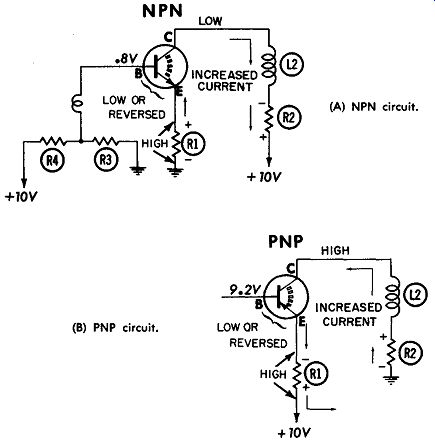
(A) NPN circuit. (B) PNP circuit.
Fig. 6-7. Effect of a leaky transistor on the circuit.
This is demonstrated in Fig. 6-7. The NPN transistor (Fig. 6-7A) has developed a partial short, causing the collector current to increase. The high collector current produces larger than-normal voltage drops across the collector and emitter resistors, causing a decreased collector and an increased emitter voltage. The base, which is tied to its voltage divider, remains fairly constant. This means the emitter voltage may rise above the base voltage, causing a reversed bias between base and emitter. The transistor should be cut off; however, collector current continues to flow through the leakage path between emitter and collector.
A signal fed into the stage will be lost because of the wrong bias polarity between base and emitter, and because the collector current cannot be controlled. The increased collector current, without proper bias, leads us to suspect a leaky transistor.
In the PNP circuit (Fig. 6-7B) a similar defect has occurred.
The partial short between emitter and collector causes increased current and the resulting increase in voltage drops across R1 and R2. This makes the collector voltages more positive and causes the emitter voltage to go down. In fact, the emitter voltage may even swing less positive than the base voltage and put a reversed bias between base and emitter. The wrong bias polarity, in conjunction with the increased collector current, causes us to be suspicious of the transistor.
High leakage is probably the most common defect in small transistors. Large power transistors usually go ahead and completely short, once they start to become leaky. Small transistors, on the other hand, very rarely develop a complete short.
Leaky transistors will not always produce a reversed bias voltage. Mild cases of leakage may cause only a reduction in the normal bias between base and emitter and in the stage gain.
Short in Base Circuit
Transformers have been known to short between primary and secondary. Although not a common defect, it has occurred several times in transistor radios. When it does happen, an unusual set of voltages is produced.
In Fig. 6-8 for example, the transformer in the base circuit has shorted. The base voltage of this stage and the collector voltage of the preceding one go to the same voltage, since they are shorted together. In our NPN circuit (Fig. 6-8A), this caused the base voltage to go very high. As a result, the transistor conducts very heavily. When the collector current goes up, so does the emitter voltage; meanwhile, the collector voltage drops way down from normal. In some circuits the emitter resistor may open because of the increased current through it.
In most low-power circuits, this will not happen. The signal, of course, will be lost.
The PNP transistor with shorted base transformer (Fig. 6-8B) will also conduct very heavily if its base voltage is lowered. Reducing the base voltage on a PNP transistor is like increasing the base voltage on an NPN transistor-the forward bias and conduction will increase. This makes all the elements go closer to the same voltage. In this respect, it somewhat resembles the open in the collector circuit discussed previously.
With an open collector circuit, however, the base voltage remained fairly near normal, whereas now it is far from normal, indicating trouble in the base circuit.
Table 6-1 lists some of the typical circuit defects and what effect they have on the voltages.
The second column in Table 6-1 shows the effect of each trouble on the transistor current flow (conduction).
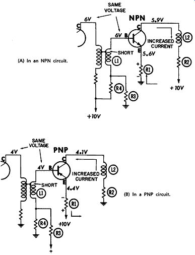
Fig. 6-8. (A) In an NPN circuit. Results of short between the primary and
secondary winding of a coupling transformer.
Note that all problems except open capacitors or detuned coils upset the collector current. This change in conduction is a tip-off that something is wrong in the DC circuit (transistor, coils, resistors, or connections).
----------------
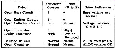
TABLE 6-1. Common Defects and Their Effects on Voltages Transistor Bias Defect Current (B to E) Other Indications Open Base Circuit
Base voltage not normal Open Emitter Circuit
Open Collector Circuit Low Normal Voltage between C&E is 0 Open Transistor of High Leaky Transistor High Low or Reversed
Detuned IF Coil Normal
Normal All DC voltages OK
Open Capacitor Normal
Normal All DC voltages OK
If emitter resistor is open there will be a voltage across it, but voltage across collector resistor will be zero.
When base or emitter is open internally. See text for open collector.
-----------------
The second column shows what happens to the voltage measured directly between base and emitter (bias). To see the bias, it is always best to measure directly between those two elements, not from element to ground. This allows you to use a lower meter range and to see the voltage more clearly. The bias measurement tells us whether the transistor is being "told" to conduct. In the first check (conduction), we learned whether the transistor was conducting. Now, we are finding out if it is being "told" to conduct, because transistor conduction depends on normal bias.
This gives us a new, more complete set of rules which will be invaluable in troubleshooting transistor amplifiers:
RULE 1--A transistor which is not conducting and not being "told" to conduct is not at fault, so look for trouble in the base or emitter circuit. (Examples: See open base circuit or open emitter circuit in Table 6-1.)
RULE 2--A transistor which is not conducting but is being strongly "told" to conduct, is probably defective. (Example: See open transistor. Check for open emitter diode.)
RULE 3--A transistor which is conducting too heavily and has low or reversed bias is probably leaky. (Example: See leaky transistor.)
RULE 4--A transistor which has lower than normal conduction and normal bias should have voltage between emitter and collector checked. If zero, collector circuit is open (see open collector circuit). If E to C voltage is normal or slightly high, the collector diode of the transistor may be open (see section on Transistor Testing).
RULE 5--A transistor stage which has all normal DC conduction but doesn't amplify properly, probably has an open capacitor or detuned coil.
Open Capacitors and Defective IF's
Open capacitors and detuned coils generally have no affect on the DC voltages, as discussed in the last section. Hence, once the trouble has been isolated to a stage, and if the voltages all check normal, it would be well to suspect a detuned coil or open capacitor. IF coils which change the radio volume when tapped or heated, or those which do not peak properly, should be replaced. Likewise, if the volume is increased when a capacitor is bridged with a good capacitor, the bridged capacitor should be replaced.
Shorted Capacitors
The effect of a shorted capacitor depends on its location in the circuit. Leaky or shorted "A" line electrolytics usually decrease all stage voltages and greatly increase the battery current drain. They also may cause motorboating or fluttering and a slight dip in "A" voltage with each flutter.
Electrolytic coupling capacitors, which couple the signal from one stage to another, can usually be spotted easily if they short. Since they are usually connected into the base circuit of a stage, the base voltage will be thrown way off when they short. Also, the voltage across the capacitor will measure zero, or much less than it should.
Other bypass capacitors, such as emitter and collector by passes, seldom short. Most shorted capacitors are confined to the electrolytic type. However, a shorted capacitor in the emitter or collector circuit would be very easy to spot because of the voltage reading there.
SAMPLE DEFECTS IN ACTUAL CIRCUITS
Now it is time to apply all of this information to an actual radio circuit. The ones we will discuss are taken from a typical transistor radio containing both NPN and PNP circuits.
NPN Stage Defects
Trouble examples in the NPN stages will be discussed first.
These stages were shown in Fig. 5-9.
Trouble: Shorted 1st IF base capacitor C2 (10 mfd). Result: Base and emitter voltages drop to zero, and the 2N253 transistor stops conducting. This causes the collector voltage to rise. The stage is very weak or is dead because there is no bias.
Trouble: Open emitter resistor RS (100 ohms). Result: The stage is dead because no current can flow. The emitter voltage rises to the base voltage or slightly above, resulting in no forward bias between the base and emitter. The collector voltage rises be cause the collector current has stopped.
Trouble: Open printed wiring between the 2N253 collector and the 7.5-ohm IF coil winding in L4.
Result: Collector current stops -flowing. The emitter voltage therefore drops to an unreadable value near zero. The collector voltage drops to the same value as the emitter voltage, and there is no difference between collector and emitter. The base voltage remains near normal. The stage is dead.
Trouble: "Leaky" 2N254 transistor in the second IF stage.
Result: The collector current goes up, and the emitter voltage rises accordingly. The emitter voltage may rise above the base voltage, since the latter stays fairly constant. The collector voltage drops only slightly because the resistors in series with the collector are small (7.5 ohms in coil LS and 220 ohms in resistor R18). The collector voltage will decrease by about 0.2 volt for each 1 milliampere of increased current. The stage will be either weak or dead, depending on how leaky the transistor be comes.
Trouble: Open capacitor across primary of IF coil LS. Result: Very weak second IF stage, with no change in voltages. The slug in IF coil LS will not peak the IF. Also, if this is an intermittent open capacitor, the radio will probably kick in when the IF can is moved or tapped, or when its lugs are heated with a small iron.
Trouble: Open secondary lead in IF coil L4, between the 2N254 base connection and voltage divider R7-R8.
Result: The 2N254 base voltage reads zero, the collector current decreases, and the emitter voltage reads zero. The collector voltage increases only slightly, not enough to be noticeable (about 0.1 volt). Be cause of the loss of bias, the signal is lost.
PNP Stage Defects
The next group of troubles refers to the PNP circuits, which were shown in Fig. 5-15.
Trouble: Open connection at the 1.2-ohm oscillator feedback coil, causing the collector circuit of the 2N252 converter to open.
Result: The collector voltage rises to assume the emitter voltage, which also rises. Conduction is low and zero voltage is read between collector and emitter.
The base voltage also rises a little because of the increased base current (but it would still be considered within normal limits). The stage is dead, and the oscillator fails to oscillate.
Trouble: Open 7.2-ohm oscillator-coil winding.
Result: The oscillator does not oscillate and cannot be heard in a nearby receiver. The voltages on the 2N252 converter read normal, except when the following test is made: When a voltmeter is set on the lowest DC scale and connected across the base and emitter leads, the 0.2-volt bias will not change as the variable capacitor is tuned across the band. The radio stage will pass noise signals easily, but no station signals will be heard.
Trouble: Open base lead inside the 2N252 converter transistor.
Result: The base voltage (at the transistor socket or solder terminal) will be fairly normal. The emitter voltage will be high (probably above 8 volts) because of loss of conduction through emitter resistor R4.
This makes a very high forward bias voltage when measured between base and emitter. The collector voltage stays at zero. The stage is dead for all signals, and the oscillator does not oscillate.
Trouble: 1,000-ohm resistor R14 in the 2N403 driver stage has a poor solder joint, making it effectively open.
Result: The base voltage reads about 7 volts. The floating emitter in the transistor "assumes" about the same voltage through the relatively low internal resistance of the emitter diodes, resulting in a loss of bias. With no collector current flowing through the 440-ohm transformer winding, the collector voltage goes to zero or ground. Audio signal is lost.
Trouble: Shorted emitter bypass C4 (40 mfd) in the driver stage.
Result: The 2N403 emitter voltage drops to zero, the transistor cuts off, and the collector voltage therefore drops to zero also. The shorted capacitor causes about nine more milliamperes of current to be drawn through resistors R14 and R18 and, as a result, an additional voltage drop of about two volts across R18. Since R18 is in the "A" line, the 8.3 volts on this line is reduced to roughly 6.3 volts.
This makes the voltages in some of the other stages appear low, and also points out the advantage of properly isolating the trouble in the beginning.
The big tipoff here is that the battery current will read 16 or 17 milliamperes, instead of the normal 7 or 8 for this radio. This would lead us to suspect a shorted electrolytic in the very beginning, and the inability of the stage to pass an audio signal would steer us to the audio section.
AM-FM Stage Defects
The same principles apply when checking AM-FM circuits; for example (refer to Fig. 4-1):
Trouble: Intermittent RF transistor in the FM tuner.
Result: In most cases, transistors which cause a radio to cut out intermittently have a bad connection on one of the leads internally, usually the emitter. This would cause the conduction to stop, and zero voltage across emitter resistor R3. Also, bias would be higher than normal. Since only the FM signals are affected when this happens (AM is normal), this leads you to suspect the FM tuner section of the radio.
Special Note: Transistors which exhibit this type of defect are often sensitive to a small amount of heat. The heat from a portable hair dryer (about 140°F) is safe, but do not use a soldering iron.
Trouble: Open IF transformer ( either AM or FM) in one of the dual purpose stages.
Result: Since the AM and FM-IF transformers are connected in series, if either one opens the radio will be dead on both bands. After checking the audio system and finding it normal, conduction is checked in each of the dual purpose IF stages. The open coil will cause the conduction reading to be either low or zero, depending on which side of the coil is open. If a primary winding is open, one of the transistors will have an open collector circuit. (Low conduction, normal bias, and no voltage between emitter and collector.) If a secondary winding is open, an open base circuit for one of the transistors will result (zero conduction, no bias).