AMAZON multi-meters discounts AMAZON oscilloscope discounts
The function of the rectifier in a power supply is to change an a-c input to a d-c output. However, the output of the rectifier is not pure direct current, but rather a series of pulses. This can be considered as being made up of two parts, a d-c component and an a-c component.
To make the output acceptable as a d-c power source, the a-c variations, known as ripple, must be removed, leaving only pure direct current. The job of removing this ripple is done by a filter.
FIG. 1 explains the operation of a simple power-supply filter. The unfiltered output from the rectifier is applied across capacitor C1. During the time the rectifier is conducting, C1 charges to the peak value of the a-c supply voltage, as indicated by line AB in FIG. lB. During the period the rectifier is not conducting and provides no output, the capacitor starts to discharge through the load, as indicated by line BC. When the rectifier once again conducts, C1 is again charged, as shown by line CD. The resulting voltage across the capacitor (the output of the power supply) is shown in FIG. 1 C. Note that the voltage is considerably smoother (less change in amplitude) than the unfiltered output of the rectifier.
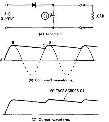
FIG. 1. Single-capacitor filter. (A) Schematic. (B) Combined waveforms.
(C) Output waveform.
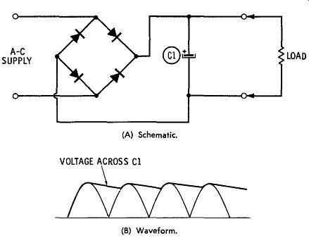
FIG. 2. Single-capacitor filter across full-wave power supply. (A)
Schematic. (B) Waveform.
FIG. 2 shows capacitor C1 connected across the output of a full wave rectifier. In this case, the power-supply output is much smoother because the capacitor discharges only half as far before being re charged by the next half-wave.
The amount the capacitor discharges between pulses is determined by the value of load connected across the capacitor. As the load resistance is decreased, more current is drawn from the capacitor while the rectifier is not conducting. As a result, the voltage across the capacitor drops more between successive "charges." This increases the variations in voltage (ripple) across the capacitor.
In FIG. 3A, no load is connected across the filter capacitor. Since no current is drawn from the filter between its successive charges from the rectifier, the voltage across it remains essentially constant.
In FIG. 3B, a load is connected across the filter capacitor. Since current is drawn from the filter between charges, the output voltage varies to a much greater extent than in the case of FIG. 3A. This variation is ripple, and the greater the voltage variation, the greater the ripple.
This simple capacitor filter is not too efficient for removing ripple from the output of the rectifier, although it does serve to illustrate basic power-supply filter action. There are several methods of improving power-supply filtering.
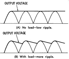
FIG. 3. Effect of loading on ripple voltage. (A) No load-low ripple.
(B) With load-more ripple.
THE CHOKE-INPUT FILTER
FIG. 4 shows an arrangement known as a choke-input filter. Here advantage is taken of the fact that the inductance of a coil tends to op pose any change in the current through the coil. Thus, the inductance of the choke, placed between the output of the rectifier and the filter capacitor, tends to oppose the build-up of current in the load when the rectifier conducts, and maintains current in the load when the rectifier is not conducting. The effect is somewhat like a flywheel, which tends to smooth out mechanical variations.
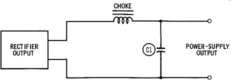
FIG. 4. Choke-input filter.
The filtering action of a choke is normally used in conjunction with a filter capacitor. FIG. 5 shows the regulating characteristics of the choke-input filter. Notice that above a certain minimum load current, the output voltage of the power supply remains fairly constant for wide variations in load. The main disadvantage of the choke-input filter is that the output voltage tends to be lower than that of other filter types.
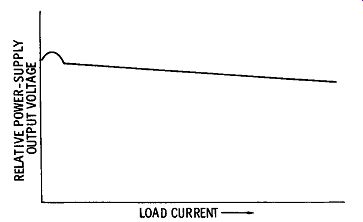
FIG. 5. Voltage regulation using a choke-input filter.
THE CAPACITOR-INPUT FILTER
FIG. 6A shows a configuration known as a capacitor-input filter.
In this arrangement capacitor C1 is placed directly across the rectifier output. Choke L1 is connected in series between the output of the rectifier and the load. A second capacitor, C2, is placed across the load terminals.
FIG. 6B shows the characteristics of the capacitor-input filter.
Note that its output voltage varies considerably with changes in load current. This type is often called a pi-section filter.
Another arrangement of capacitor-input filter is shown in FIG. 7.
Here a resistor is substituted for the choke between input and output filter capacitors. The use of this resistor-capacitor filter provides acceptable filtering in low-current circuits where a physically larger, more expensive filter choke is not possible. This arrangement is found in most a-c-d-c radios, audio preamps, etc.
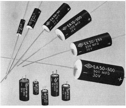
A typical filter capacitor used in connection with tube circuits.
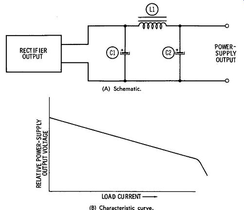
FIG. 6. Voltage regulation using a capacitor-input filter. (A) Schematic.
(B) Characteristic curve.
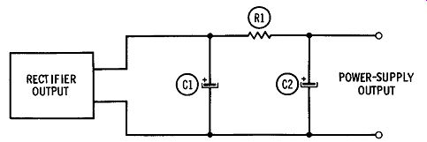
FIG. 7. Resistor-capacitor filter.
POWER-SUPPLY VOLTAGE REGULATION
In most cases the voltage at the output terminals of a power supply varies as the current in the load changes. This variation is referred to as the regulation of the power supply. The less the change in output voltage for changes in load current, the better the regulation is, and the better the power supply is. Regulation is generally expressed as a percentage and may be calculated from the following formula:
. _ (no load voltage) - (full load voltage)
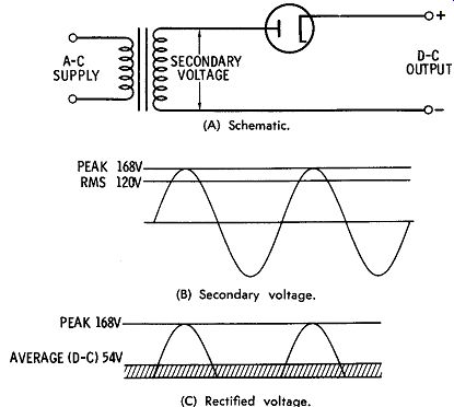
FIG. 8. Half-wave rectifier. (A) Schematic. (B) Secondary voltage.
(C) Rectified voltage.
OUTPUT VERSUS INPUT
For a given secondary voltage, the resulting d-c output voltage of a transformer power supply depends on several factors, including the type of rectifier circuit, type of filter, and load. There are several difference rectifier circuits. In the half-wave rectifier shown in FIG. 8, the peak d-c voltage output (before filtering) is the same as the peak secondary voltage-1.4 times the rms value. If the secondary voltage is 120 volts rms, the peak output voltage is 120 x 1.4, or 168 volts.
The average d-c output voltage' of this same half-wave rectifier is 0.318 times the peak voltage. Since this peak is 168 volts, the voltage appearing at the output terminals is 168 x .318, or approximately 54 volts.
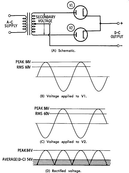
FIG. 9. Full-wave rectifier. (A) Schematic. (B) Voltage applied to
V1. (C) Voltage applied to V2. (D) Rectified voltage.
Thus, when the full-wave and half-wave circuits are compared, the d-c output is the same if the secondary voltage (but not the voltage across the rectifiers) is the same.
In the case of the bridge rectifier shown in FIG. 10, the average output voltage will be 0.9 times the applied secondary rms voltage, or .637 times the peak voltage. The peak output voltage of the bridge rectifier is 1.4 times the rms input voltage.
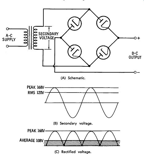
FIG. 10. Bridge rectifier. (A) Schematic. (B) Secondary voltage. (C)
Rectified voltage.
For a given output voltage from the rectifier, the voltage developed at the output of the filter will depend on the particular filter configuration. Refer for a moment to the basic single-capacitor filter in Fig. 11A. When the rectifier conducts, capacitor C1 charges to the peak value of the rectifier output voltage. During the time the rectifier is not conducting, C1 retains essentially all of its charge if there is no load connected across it.
When a load is connected across its terminal, C1 partially discharges during the periods when the rectifier is not conducting. The amount of this discharge, of course, depends on the amount of load-the discharge increasing as the load is increased. The same characteristic holds true in the case of a multisection capacitor-input filter such as the one shown in FIG. 11B. From all this, you can see that the d-c output voltage of a capacitor-input filter approaches the peak value of the rectifier output voltage with small values of load, the output voltage dropping as the load is increased.
above: Small electrolytic capacitors used with transistor circuitry.
If a choke-input filter is used ( FIG. 11C), the voltage across the output terminals is the average value of the voltage appearing at the rectifier output.
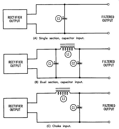
FIG. 11. Filter configurations. (A) Single section, capacitor input.
(B) Dual section, capacitor input.
(C) Choke input.
REDUCING OUTPUT VOLTAGE
Often, it is necessary to reduce the output voltage of a power supply to some other value. For example, the screen-grid voltage of a tube frequently must be lower than the plate voltage.
There are two principal methods of dropping voltage-series resistance and voltage division. FIG. 12 illustrates the idea of voltage dropping by series resistance. Resistor R1 is placed in series with the filtered d-c supply and the load requiring the lower operating voltage.
The value of R1 is determined by (1) the amount of voltage to be dropped across it, and (2) the amount of current drawn by the load.
All this is summed up in Ohm's law: E R=y where, R is the value of dropping resistor, in ohms, E is the desired voltage drop across the resistor, in volts, I is the current drawn by the load, in amperes.
As a practical example of this, assume we have a tube that requires a plate voltage of 140 volts. At this plate voltage, the tube draws a plate current of 20 ma. The output from the power supply is 300 volts.
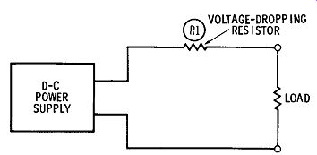
FIG. 12. Series voltage-dropping resistor.
To determine the correct value of the series-dropping resistor, Ohm's law is applied as follows:
R
= E = (300 - 140) = 8
000 h I (.02) ' o ms
The power that must be dissipated by the series-dropping resistor is easily determined by the formula: W=I2R where,
W is the power, in watts, I is the value of current in the resistor, in amperes, R is the value of series resistance, in ohms.
In the previous example, the power dissipated by the series-drop ping resistor would be:
W = .022 X 8000
= 3.2 watts
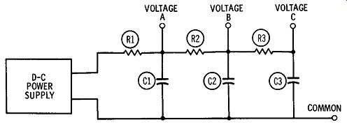
FIG. 13. Decoupling network.
A variation of the series-dropping resistor arrangement is shown in FIG. 13. This configuration, often called a decoupling network, uses filter capacitors C1, C2, and C3 at the junction of series-dropping resistors R1, R2, and R3. A number of different voltages can be obtained by this arrangement, and the presence of the additional capacitors improves the overall filtering.
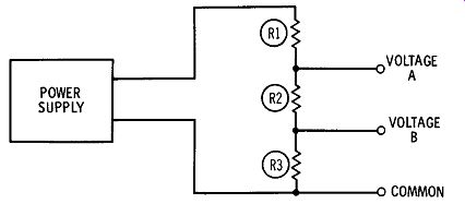
FIG. 14. Voltage divider.
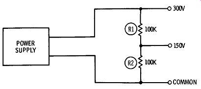
FIG. 15. Practical voltage divider.
The voltage divider is another widely used method of voltage drop ping. Several series resistors, R1, R2, and R3, are connected across the output of the power supply, as shown in FIG. 14. The values of R1, R2, and R3 are selected to provide the desired voltages between their junctions (A and B) and common. As many resistors as needed may be connected in series to obtain a wide selection of output voltages. When only a negligible amount of current is drawn from the taps of a voltage divider-as for example, the bias of a class-A amplifier-the voltage at the resistor taps is proportional to the ratio of the resistance. In the voltage divider shown in FIG. 15 the voltage at the junction of R1 and R2 is 150 volts when equal-value resistors are used for R1 and R2.
When significant current is drawn from the taps of a voltage divider, the following formula may be used to determine the individual resistance values, using the configuration shown in FIG. 16:
The number of series-connected resistors and taps may be extended to any desired number by expansion of the above formula. The value of 13 can be assumed to be 10 percent of the total load current of all taps.
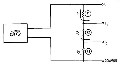
FIG. 16. Voltage divider.
PRACTICAL CIRCUITS
The following circuits, although simple, are handy as a source of operating power for radio receivers, small amplifiers, preamps, etc.
All of them utilize a power transformer for maximum safety of operation. The primary and secondary windings are isolated, so neither side of the d-c output is connected directly to the power line. As a result, there is no "hot-chassis" problem to cause a possible shock.
A Simple Half-Wave, Low-Current Power Supply
The half-wave power supply in FIG. 17 is capable of furnishing a d-c output of 120 volts at an output current of 50 ma. Actually, with light loading the output voltage will rise to nearly the peak value of the input volts (168 volts) because of the use of a capacitor-input filter. In addition to the d-c output, this supply also furnishes a 6.3 volt a-c supply at a current rating of 2 amps.
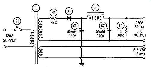
FIG. 17. Half-wave power supply.
-----------------
Parts List for FIG. 17
Item No. Description
C1 Capacitor, 40 mfd, 150 volts, electrolytic
C2 Capacitor, 40 mfd, 150 volts, electrolytic L1
Choke, 16 hy, 50 ma (Stancor (1003, or equivalent)
R1 Resistor, 47 ohms, 1 watt
R2 Resistor, 1 megohm, ½ watt
S1 Switch, spst
T1 Transformer, power.
Secondaries: 125 volts, 50 ma; 6.3 volts, 2 amps (Stancor PA8421, or equivalent)
X1 Rectifier, silicon, 1N2483
--------------------
FIG. 17 is the power-supply schematic. An a-c input of 120 volts rms from the power line is applied to the primary of power trans former T1. The a-c voltage developed across the secondary of T1 is applied to silicon rectifier X1. Resistor R1, connected between the top of the secondary and X1, serves to limit the surge current through X1 when filter capacitor C1 charges during initial application of power to the unit.
The output of the silicon rectifier is applied to the two-section capacitor-input filter consisting of C1, L1, and C2. Resistor R2, connected across the output terminals of the filter, serves to discharge the capacitors when power is removed from the supply. Without R2, the charge retained by C1 and C2 can provide an unpleasant "surprise" if the power-supply output terminals are accidentally touched.
A Full-Wave, Medium-Current Power Supply
The supply in FIG. 18 is designed to provide a higher current than the unit just described. It has a d-c output voltage of 350 volts at a current of 90 ma. This voltage will rise to more than 450 volts under light loading conditions because a capacitor-input filter is used. In addition to the d-c output, this supply also furnishes 6.3 volts of alternating current at a rating of 3 amps.
In operation, a-c line current is applied to the primary of power transformer T1. The high-voltage developed across the secondary of T1 is rectified by the full-wave rectifier tube, V1. The output of V1 is applied to the double-section capacitor-input filter consisting of C1, LI, and C2. Resistor R1, placed across the output of the filter, serves to discharge C1 and C2 after power has been removed from the supply.
A Voltage-Doubler Power Supply
FIG. 19 is the schematic of a half-wave doubler power supply.
Depending on the load, this supply will put out between 200 and 300 volts. Maximum rated load current is 25 ma. A separate 6.3-volt a-c output at 5.5 amperes is also provided.
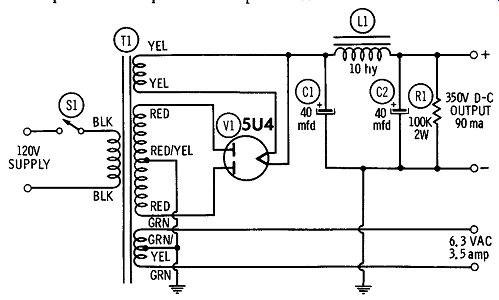
FIG. 18. Full-wave power supply.
Parts List for FIG. 18
---------
Item No.
C1 C2 L1 R1 S1 T1 V1
Description
Capacitor, 40 mfd, 450 volts, electrolytic
Capacitor, 40 mfd, 450 volts, electrolytic
Choke, 10 hy, 90 ma (Knight 54D4707, or equivalent)
Resistor, 100K ohms, 2 watts
Switch, spst
Transformer, power.
Secondaries: 700 volts center-tapped, 90 ma; 5 volts, 3 amps; 6.3 volts, 3.5 amps (Knight 54D2043, or equivalent)
Tube, 5U4
----------
Referring to the schematic, the a-c line current is applied to the primary of power transformer T1. The resulting voltage developed across the high-voltage secondary is applied to the voltage doubler, which consists of X1, X2, C1, and C2. The output of the voltage doubler is filtered by C2, L1, and C3. Resistor R2 discharges the filter capacitors when power is removed from the unit.
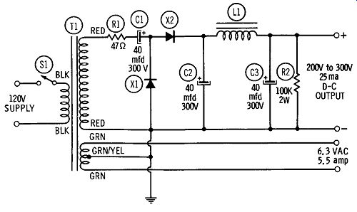
FIG. 19. Voltage-doubler power supply.
----------------
Parts List for FIG. 19
Item No.
C1 C2 C3 L1 RI R2 SI T1 XI X2
Description
Capacitor, 40 mfd, 300 volts, electrolytic
Capacitor, 40 mfd, 300 volts, electrolytic
Capacitor, 40 mfd, 300 volts, electrolytic
Choke, 10 hy, 90 ma (Knight 54D2139, or equivalent)
Resistor, 47 ohms, 1 watt
Resistor, I00K ohms, 2 watts
Switch, spst
Transformer, power.
Secondaries: 135 volts, 200 ma; 6.3 volts, 5.5 ma (Knight, 54D3708, or equivalent)
Rectifier, silicon, I N2613 Rectifier, silicon, I N2613
--------------------------
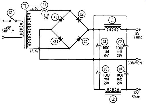
FIG. 20. Transistor power supply.
--------------
Parts List for FIG. 20
Item No.
C1 C2 C3 C4 L1 L2 R1 S1 T1 X1 X2 X3 X4
Description
Capacitor, 1000 mfd, 25 volts, electrolytic
Capacitor, 1000 mfd, 25 volts, electrolytic
Capacitor, 1000 mfd, 25 volts, electrolytic
Capacitor, 1000 mfd, 25 volts, electrolytic
Choke, .035 hy, 2 amps (Knight 54D2343, or equivalent)
Choke, 16 hy, 50 ma (Knight 54A2137, or equivalent
Resistor, 4.7 ohms, 2 watts
Switch, spst
Transformer, filament, 12.6 volts, 1.5 amps (Knight 54D4136, or equiv.)
Rectifier, silicon, 1N1081
Rectifier, silicon, 1N1081
Rectifier, silicon, 1N1081
Rectifier, silicon, 1N1081
-------------
Low-Voltage Power Supply
In FIG. 20 is a power supply that is ideal for furnishing operating voltages for transistor circuitry. Supplying 12 volts at 1 ampere, the unit will furnish sufficient current for most conventional transistor circuitry. An additional output, also 12 volts, with a maximum current of 50 ma is available. This latter output has much better filtering be cause of the additional filter element. It is useful where an output of extremely low ripple is required.
As shown in FIG. 20, operating power is applied to the primary of power transformer T1-actually a 12-volt filament transformer.
The voltage developed across the secondary is applied to the full-wave bridge rectifier consisting of X1, X2, X3, and X4. The d-c output of the bridge rectifier is fed to the two-section capacitor-input filter C1, L1, and C2. The output from this filter is fed to the 12-volt, I-ampere output terminal. An additional filter, consisting of L2, C3, and C4, provides further filtering. The output of this filter is available at the 12-volt, 50-ma output terminals.
Also see: