AMAZON multi-meters discounts AMAZON oscilloscope discounts
Separate sections of this guide cover RF's, IF' s, audio sections, power supplies, oscillators, and many other circuits used in radio and television receivers. This section shows and describes an assortment of circuits, including transistorized video amplifiers, video detectors, deflection circuits, and diode detectors and clippers.
VIDEO DETECTORS
High-frequency transistorized video detectors are made possible by using MADT and SBT transistors. A typical common emitter circuit is shown here, along with the formula for power gain.
Detection takes place because the transistor amplifies only half the IF input waveform. A filter in the collector circuit separates the IF carrier from the modulation information. Power gain for a detector is figured as shown in the diagram, where Eo is the audio-output voltage for a 30% modulated input signal, and Ee is the magnitude of the unmodulated input signal. Diode detection results in a 14-db signal loss in broadcast IF detectors. however, the use of an SBT results in over 5 db of signal gain, and an MADT will provide a gain of over 15 db.
This circuit can be used as a detector with either a 455 -khz or 45 -mhz input. The only factor to consider is the value of C2. As used in this circuit, an SBT will yield about 1 db of gain and an MADT over 5 db, as opposed to the 14-db diode-detector loss.
Desirable characteristics for good transistor detectors are high amplification at the operating frequency and a low output impedance. SBT's and MADT's provide these conditions. In addition to being a good detector, this circuit is a good source of AGC be cause of the gain it provides.
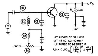
------------- Video detectors.
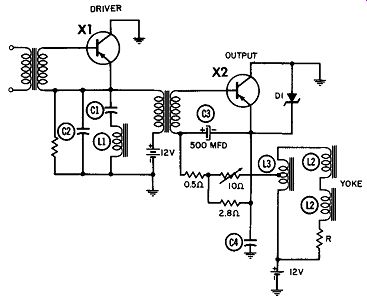
-------------- (A) Horizontal circuit.
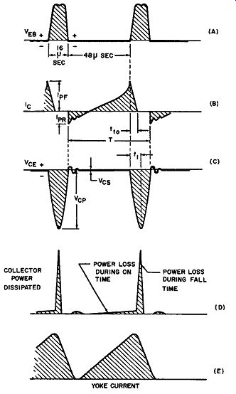
--------------- (B) Waveform. TV horizontal-deflection system.
TV HORIZONTAL-DEFLECTION SYSTEM
Switching transistors can be used for horizontal deflection in a TV receiver. Part A of the diagram shows a switching transistor circuit, and Part B the waveform of various parts of the circuit.
Three 0.24-ohm wirewound resistors in parallel were used to read the current waveforms shown.
Driver X1 turns X2 on for about 48 µ-secs and off for 16 µ-secs.
Because of the reverse-biased zener diode across the transistor, a current flows in the reverse direction for the first 9 µ-secs. After this initial 9 µ.sec current How, 39 µ.secs is required for the collector current to build up to its peak forward value. At the end of this period, the base of X2 is driven positive, thus reducing the collector current to zero. This collapsing current induces a high voltage across the yoke during retrace. Capacitor C4, in resonance with L3, tunes this circuit to a frequency of ½ tr ( where tr is the retrace time). As this collapsing voltage passes through 180° and becomes positive, the base is again pulsed and current flows; thus the full 360° cycle is completed. In the driver stage, C1 and L1 form a resonant circuit at the third harmonic of the retrace frequency, to reduce the peak voltage from collector to emitter of XL With this circuit, the peak voltage of 90 to 110 volts is reduced to 80 or 90 volts. This reduction affects only the driver, not the output, stage.
The stage gain of X2 can be improved by returning the energy to the battery through bilateral action of the transistor. At the end of the retrace cycle, the collector voltage begins to swing positive.
The base and collector currents will be high, being limited only by the transistor saturation and lead resistances. However, these currents will decay rapidly to zero because of the damping effect of the transistor on free oscillations. Thus, part of the energy stored in the yoke during the forward sweep is returned to the battery.
Important requirements of output transistor X2 are high efficiency and the ability to withstand high reverse voltages. The 2N629 and 2N630 series fulfill these requirements. If the yoke is designed to give a higher voltage than the transistor can stand, the collector-to-emitter voltage can be clipped to a safe level by using a 10M91Z zener diode. It is a good idea to use the diode anyway, because it affords excellent transistor protection.
DIODE LIMITERS
Part A of the diagram shows two diodes connected in series with their polarities reversed in order to utilize their zener breakdown characteristics. for limiting action. Balance of the output voltage may be controlled by selecting proper diodes, each with a particular zener-voltage level. For special applications, two diodes having substantially different zener voltages may be used to deliberately unbalance the output.
The voltage level may be reduced by using a resistive divider.
This divider is very effective when the clipped and reduced signal is to be fed to a high-impedance load such as a vacuum-tube grid. When considerable current must be supplied to a load, it might be necessary to select diodes that have suitable zener voltage levels ( IN465 through IN470) and use them without a resistive voltage divider. However, some sharpness of clipping action will be sacrificed in going to lower zener voltages.
As shown in Part B of the diagram, two diodes may be connected in parallel and their polarities reversed in order to utilize their steep forward characteristics for limiting action. The peak to-peak output voltage will range from approximately 1 to 2 volts, depending on the value to which RI limits the current. Here two IN138A diodes are recommended where the peak current through R1 is less than 1 ma.
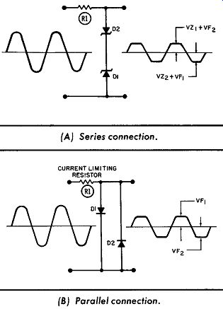
------------ Diode limiters.
(A) Series connection.
(B)Parallel connection.

-------------------- Backward diode detector.
BACKWARD DIODE DETECTOR
This illustration shows a Uni-Tunnel (backward) diode used as a detector. In this circuit the 10 -mhz input is modulated by a 0.4-volt peak-to-peak, 100 -khz signal, while a 0.2-volt detected signal is present across the output circuit.
HIGH INPUT-IMPEDANCE VIDEO AMPLIFIER
This diagram shows a 2N1493 and 2N274 in a typical video amplifier circuit employing negative feedback. The frequency response is 20 cycles to 7.5 megacycles ( 15-mmf load), the voltage gain is 75, and the input resistance is 5,000 ohms. This circuit may be used in industrial-television video amplifiers, instrument amplifiers, or pulse amplifiers.
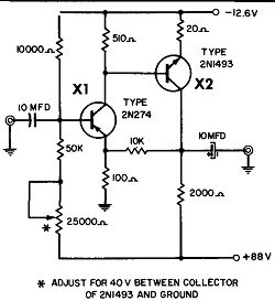
------------ High input impedance video amplifier.
VIDEO AMPLIFIER
Special processing techniques for high-frequency transistors allow design of transistorized video amplifiers. A two-stage video amplifier without feedback is shown in Part A of the diagram.
With all coils grounded, the amplifier is an RC-coupled common emitter circuit. The output impedance of the circuit is essentially the same as the input impedance. A stage gain of 5 and a band width of 5 mhz are considered typical. The addition of L3 and L4 improves the bandwidth gain 50%, and L1 and L2 improve it another 30% by decreasing the loading effect of the resistor at the high end of the band. These circuit values were chosen be cause they aid the gain at 3 mhz and above.
Part B shows a video amplifier with feedback. Through the use of series peaking coil L3 and feedback, its bandwidth gain can be made to approach the theoretical limit of the transistor used.
With transistors having a cutoff at 45 me, the bandwidth is vari able from 12 to 20 me, with a corresponding gain variation from 14 to 40 db. Cascading of such feedback amplifiers is possible without interaction, because feedback is independent of the load.
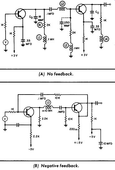
-------------- Video amplifiers. (A) No feedback. (B) Negative feedback.
--------------
VOLTAGE-DOUBLER VIDEO AMPLIFIER-DRIVER
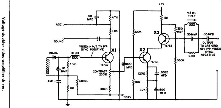
This figure shows an application of three MADT transistors in a video-amplifier voltage-doubling circuit. Bandwidth realized is that normally required for TV receivers.
Following the IN60A diode detector, video input to the first amplifier base is 0.7 volt peak-to-peak, sync positive. Sound and AGC are taken off the collector as shown. From the 250-ohm contrast control in the emitter circuit, the video information is amplified by two direct-coupled stages. The output to the picture tube grid, after the 4.5 -mhz trap, is 55 volts peak-to-peak with video sync negative.
TV DEFLECTION
A single-transistor deflection circuit is shown here. Because of its fast switching time and high voltage gain, the 2N1073B is the first transistor found useful for horizontal-deflection circuits.
The low saturation resistance of the 2Nl073B provides good waveform linearity.
The B-201 rectifier is a high-speed, low forward-drop diode used for the reverse-current swing of the yoke. The drive to the circuit is adjusted for +L5 volts maximum. The base-to-emitter voltage varies from -0.5 to + 1.5 volts, resulting in a peak current of 2 amperes as shown by the waveforms.
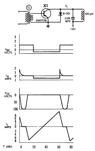
---------------- TV deflection.
FLEAPOWER SOLAR-CELL CIRCUITS
Some very simple electronic circuits are possible using solar cells. Here, three circuits are shown which represent an extremely low-power application for photovoltaic cells. Two of the circuits shown are oscillators, and each is designed for operation using a single photocell as its power supply.
Either photocell requires much less illumination than direct sunlight. Good room illumination, of at least 100 foot-candles, will furnish the required electrical energy. In Part A of the diagram, the output frequency of the wide-range audio oscillator ( multi vibrator) may be varied by potentiometer R3. Any frequency between 1 and 1,000 hz may thus be obtained.
This circuit is an asymmetrically coupled multivibrator with its period of oscillation determined by R1, R2, R3, C1, and C2.
All these components are non-variable except R3, which serves as the frequency control.
R3 adjusts the frequency by causing a corresponding variation in the coupling between the output of X1 and the input of X2.
The output of this circuit is a rectangular wave. For good frequency stability, the illumination on the photocell should remain constant. The output of the oscillator may be increased by using two or more photocells in series.
This handy audio oscillator may be found useful in servicing all kinds of circuits. It can also be used as a code-practice oscillator.
In Part B an audio oscillator with inductive feedback is shown.
This oscillator can be used for the same purpose as the one shown in Part A. In this circuit the output frequency is determined by the degree of illumination, with approximately 100 foot-candles required for proper operation. Oscillation occurs as a result of positive feedback obtained from transformer coupling.
One possible use for this device is as an exposure meter in photography, where the output frequency is an indication of the light level measured.
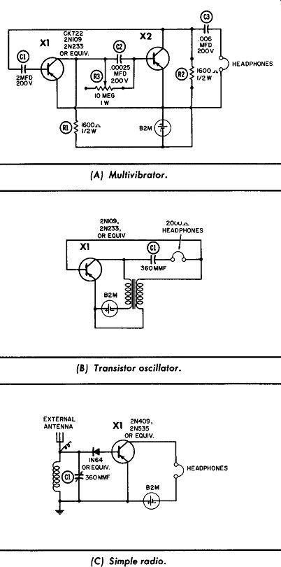
------------- XTERNAL ANTENNA (A) Multivibrator. HEADPHONES. (B) Transistor
oscillator. (C) Simple radio. Flea-power solar-cell circuits.
Part C shows a simple sun-powered radio. It is designed to work with a single B2M sun-battery cell requiring very low illumination. The circuit uses a small number of components, and re quires only 10 foot-candles of illumination incident on the photo cell for proper operation. This will produce good volume in an ordinary pair of 2,000-ohm headphones. However, the sensitivity and selectivity will only allow it to receive strong local stations.
Under optimum conditions, the radio will drive a 4-inch PM speaker satisfactorily. In this case the highest impedance primary terminals of a universal output transformer should be connected in place of the headphones, and the speaker should be connected across the low-impedance secondary winding.
By varying the capacitance of C, any desired frequency in the standard broadcast band can be picked up. A loopstick primary can be used as the antenna, and an extra length added for better performance if desired. A good earth ground will also do much toward improving the performance.
TV / FM TUNED AMPLIFIER
This is a micro-alloy diffused-base transistor ( MADT) RF amplifier used for FM or TV applications. Its performance is given below:
Center 3-Db RF RF Noise Channel Frequency RF Gain Bandwidth
Figure (Mc) (Db) (Mc) (Db)
13 213 10 10 9 10 195 11 10 8 6 85 16 8 4 3 63 18 7 3
The 45 -mhz trap in the base circuit of the amplifier is designed to prevent any signal lower than that of Channel 2 from entering the circuit. This improves the rejection of the amplifier.
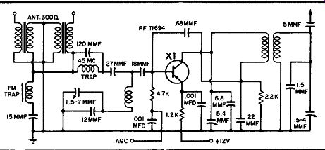
----------------- TV/FM tuned RF amplifier.
DIODE CLIPPERS
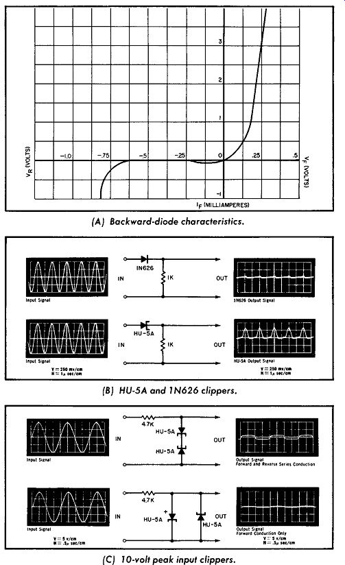
------------------------ (A) Backward-diode characteristics. (B) HU-SA and 1N626
clippers. (C) 10-volt peak input clippers. Diode clippers.
Either the backward or reverse tunnel diode can be used in a clipper and rectifier circuit. Part A of the diagram shows the characteristics of a typical backward diode, and Part B compares the HU-5A Uni-Tunnel diode with a 1N626 fast-recovery silicon junction diode. This comparison is made with a 500-millivolt AC input signal.
As shown by the output waveforms, the peak rectified voltage across the Uni-Tunnel (backward diode) exceeds 250 millivolts, and is far greater than the voltage across the silicon-junction diode. By using a 0.2-mfd capacitor across the 1,000-ohm output load in each circuit, the lower diode will have a DC output of 200 millivolts, whereas the ordinary diode will have an output of only 10.5 millivolts.
A 10-volt peak-input clipping circuit that can be used either to form a square wave or as a limiter is shown in Part C. The output waveforms in the diagram show the circuit action for both the upper and lower circuits.
455-khz CONVERTER
This figure shows a broadcast-band IF-converter circuit. The input and local-oscillator signals are mixed at the base-emitter junction, and the collector circuit is tuned to the difference frequency. The collector is thus grounded at the local-oscillator and signal frequencies, and the emitter and base are essentially grounded at the difference frequency. Therefore a gain occurs from emitter to collector. The typical conversion gain of such a stage is 20 db, with a noise figure of 4 db.
Although the circuit performs well at broadcast frequencies, its range of usefulness as a converter extends much further. By employing a micro-alloy diffused-base transistor ( MADT), the complete range of VHF television frequencies can be covered satisfactorily.
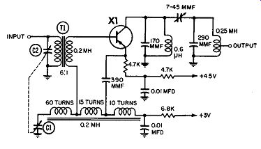
----------- 455 -khz converter.

-------------
CITIZENS-BAND TRANSCEIVER
This diagram shows an experimental all-transistor Citizens band transceiver. This transceiver is not intended for use with FCC Part 15 rules ( which limit the power output to 100 milli watts), but rather with regular Class-D CRS rules.
In the receiver arrangement, a super-regenerative detector ( X1) that provides a sensitivity of approximately two microvolts is used. This detector quenches ( goes in and out of self-oscillation) at a 40-khz rate. The low-pass four-section filter in the output circuit removes both the 27-mhz and 40-khz components of the output signal, thus allowing only audio to pass. A three-stage audio amplifier feeds a push-pull output. This output uses S-3001 (version of the 2N698) transistors, although many other types of NPN audio transistors will work equally well.
In the transmitting arrangement, the crystal mike is used for modulation, with the level being set by a 10K-ohm pot at the output of the first amplifier. An S-3001 crystal-controlled oscillator, in common-base operation, provides an RF drive of 100 milliwatts to the final. The three final transistors in parallel provide 500 milliwatts of output to the antenna. These finals are operated as common-base amplifiers with collector (high-level) modulation taken from the audio-output transformer.
Either a 12-volt battery or an appropriate external power sup ply can be used. The transceiver range is about one-half to two miles. Power consumption is about 1.8 watts for the transmit and 350 milliwatts for the receive mode.
(Note: This is an experimental unit. It is not licensed and, under current FCC rules, cannot be used without certification.)