AMAZON multi-meters discounts AMAZON oscilloscope discounts
Because transistors and semiconductor diodes are two-state devices, they are well suited for use in logic circuits. A vacuum tube, on the other hand, requires heater and plate supplies. Thus, it uses a great deal of power even as a simple on-off device. A semi conductor device can perform the same function with as little as one hundredth of the power.
Logic circuits operate on a "go, no-go" basis; that is, they have two recognizable states-on or "one," and off or "zero." There are many ways of establishing these two states. The most common are ( 1 ) to use pulses or ( 2) changes in voltage of current level. In the absence of a pulse or a change in the input level, the circuit is in its "zero" state. Application of an input pulse changes the state to indicate a "one." Many types of circuits can be used for on-off operation; the problem is that they must be used in large number in order to form arithmetical units capable of counting multi-digit numbers ( as required of a digital computer, for example). Several circuits may feed into one, or one circuit may feed several others; thus, circuit design is somewhat restricted.
Two basic circuit types are described in this section; one is defined as AND, the other as OR. In an AND circuit, there is an output if ( and only if) both elements conduct, just as two switches in series must both be closed before current can flow.
On the other hand, OR circuits are like two switches in parallel, where current will flow if either is closed ( or if both are).
THE SCR AS A STATIC SWITCH
The input characteristics of the CS or SCR, gate-to-cathode, are similar to the base-emitter input of the NPN silicon transistor.
Firing occurs at specific values of input current and voltage.
Thus, the device can be used as a static switch with either an AC or DC source.
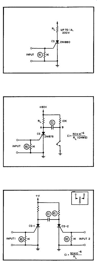
---- (A) Simple latching switch.
(B)Shunt capacitor turn off.
(C) DPDT static switch.
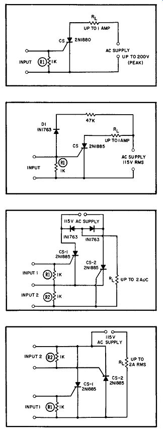
(D) Half wave switch.
(E) AC static switch.
(F) Full-wave static switching.
(G) Full-wave output.
The SCR as a static switch.
Circuit A has a DC source, and the CS acts as a latching switch. Once turned on by a control signal, it will remain on. To turn it off, the anode current must be reduced below the dropout level. Resistor R1 provides a negative-gate bias current and insures a stable "off" condition. Less than 20 microwatts of input power ( 0.6 volt, 20 µ.a) for 1 microsecond or longer is required to turn on a load power of up to 200 watts. By proper choice of R1, the sensitivity can be reduced even further.
The CS will latch on at any load current above the dropout level. It will work as well with small loads ( 10 ma) as it does at higher load currents. The circuit can be used as a single-contact latching switch for direct control of a given load, and is useful for driving relay coils or similar electromagnetic loads. With the CS, an ordinary DC relay can be converted to a high-sensitivity latching relay. For inductive loads a shunt diode may be required, to eliminate a voltage surge when the power is removed.
For the simple latching circuit, turn-off can be accomplished by removing the source voltage. The CS can also be turned off through use of a capacitive shunt, as in circuit B. The CS is off until an input control signal turns it on. When on, the voltage at the anode is about one volt. C1 charges through R2 to about the value of the supply voltage. Closing the switch causes the charge across the capacitor to drive the CS anode negative with respect to ground. Load current is no longer supplied by the CS, but from the discharging capacitor. This method of achieving CS cutoff is known as shunt-capacitor turn-off. The capacitor must be sufficiently large to hold the CS anode negative long enough to insure turn-off.
As shown in circuit C, another CS can be used in place of the switch. Turn-off is accomplished in the same manner, except that a momentary low-level positive pulse is required at input 2.
This circuit is actually a power flip-flop. When CS-1 is turned on (by a suitable input signal), CS-2 is turned off by the resultant voltage drop coupled through C1. When CS-2 is turned on, CS-1 is turned off. R1 can be replaced by a second load so that DPST switching between the two loads becomes a simple matter of applying low-level pulses to the appropriate inputs.
With an AC voltage source, the CS performs as a controlled half-wave rectifier, blocking both the positive and the negative half-cycles until a positive control signal is applied to the gate. The CS will then conduct during the positive half-cycles. By proper timing of the applied control signal, the CS can be made to conduct during all or part of the positive half-cycle. Thus, pro portioning control of the output is possible, as well as on-off switching.
Circuit D is a simple AC static switch which supplies rectified half-wave DC to the load. The input control signal can be AC, DC, or a pulse. If the load is inductive, shunting it with a diode will supply continuous current through the load during the negative half-cycle. The inductive field built up during the positive half-cycle will return stored energy during the negative alternation. The diode polarity permits this current to How in the same direction as during the positive alternation.
In AC circuits, the positive control voltage applied to the CS gate must be kept low during the negative half-cycle because of reverse leakage current, which increases along with the positive gate current. If this leakage current becomes large enough, it can cause thermal runaway. The reverse half-cycle leakage current is about half the positive gate current; by use of R2 and D1 ( as shown in circuit E), a bucking current can be obtained to cancel the effect of any reverse leakage current during the negative half-cycle.
Full-wave static switching is also possible. As shown in circuit F, a full-wave DC circuit can be formed by using two CS stages in a bridge rectifier. Input 1 is applied when CS-1 has a positive anode voltage; during the next alternation, input 2 is positive while the anode of CS-2 is positive. Any output from maximum to zero is possible. For
PNPN TRIGISTOR PULSE-DURATION SWITCH
Acting as a signal switch, the PNPN Trigistor unit has a number of uses. It is particularly suited to memory, counter, gating, timing, logic, and related pulse applications. These functions are usually achieved by combining one or more of the basic bistable circuits shown with appropriate coupling networks.
These basic circuits show some of the possible variations which can be used to obtain a choice in triggering and output points.
In all these circuits, the Trigistor is turned on by making the base more positive than the emitter. Cutoff is achieved by making the base more negative than the emitter, or by reducing the collector current below the holding value. The Trigistor has a preferred off state, which it assumes before any base pulses have been applied.
Both turn-on and turn-off are accomplished at the base in circuit A. The output is taken directly across the Trigistor. output-pulse width is determined by the time between input pulses and is independent of input-pulse widths. Thus, this circuit can provide a pulse output of variable delay.
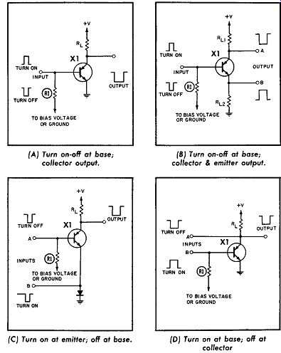
-------- PNPN Trigistor pulse-duration switch. (A) Turn on-off at base; collector
output.
(C) Turn on at emitter; off at base.
(B)Turn on-off at base; collector & emitter output.
(D) Turn on at base; off at collector
The circuit shown in B is essentially the same except that outputs are available from both the collector and emitter, thereby providing pulse outputs of both polarities. Input-voltage requirements for both turn-on and turn-off must increase ( over that required by the first circuit) by an amount equal to the output voltage at the emitter.
Only negative triggering pulses are used in circuit C. Turn-on is accomplished by applying a negative pulse to the emitter, across a silicon diode in the inverse direction. A diode is used in place of a resistor because its impedance becomes very low when the Trigistor is on. Turn-off is accomplished by 'applying a negative pulse to the base. The output is the same as for circuit A. Circuit D is also similar to A except that turn-off is accomplished by driving the Trigistor collector negative. Almost all the collector current must be bypassed for turn-off to take place.
Determining the proper component values for use in basic Trigistor circuits is not difficult. The collector resistor and B+ voltage determine the "on" current level. Between 3 and 5 ma will insure best Trigistor performance throughout the operating temperature range. B+ voltages as low as +3 volts can be used.
It is desirable, however, to use a B+ value well above this lower limit so the circuits will not be sensitive to small voltage changes.
When the Trigistor is off, the collector cutoff current can act as a positive-gate current signal, tending to turn the Trigistor on.
The base resistor RB provides bias current to insure a stable "off" condition. For operation up to 125°C., the bias-off current should be a minimum of 150 microamps. Thus, if a bias-voltage source of - 1.5 volts is used, the base resistor should be 10K or less.
STAIRCASE-WAVE GENERATOR
--------- Staircase wave generator.
Here is a simple staircase-wave generator which has good stability and a wide operating range. Unijunction transistor X1 operates as a free-running oscillator which generates negative pulses across R2. The resultant conduction cycles of X2 charge capacitor C1 in steps. When the voltage across C1 reaches a level which will cause X3 to conduct, this transistor fires and discharges C1.
Resistor R1 determines the frequency of the staircase wave form, and resistor R2 determines the number of steps per cycle.
As shown, the circuit can be adjusted for an output frequency from 100 hz to 2 khz, and the number of steps per cycle can be adjusted from one to several hundred. This circuit can also be adapted for use as a frequency divider by adding stages in cascade, similar to the hook-up between X2 and X3.
TUNNEL-DIODE SHIFT REGISTER
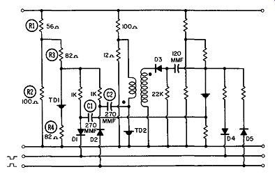
This shift-register circuit uses two monostable tunnel diodes and three backward diodes per stage.
Assuming that stage TD1 is in the high-voltage state, diode D1 becomes forward-biased whenever a negative-going pulse is applied. This pulse is therefore passed, via capacitor C1, to the cathode of TD2, switching it to the high-voltage state.

--------- Tunnel-diode shift register.
If the first stage is in the low-voltage state, a positive-going pulse will be applied, via backward diode D2 and capacitor C2, to the anode of TD1. This positive pulse will drive TD1 into the high-voltage state. The resultant positive voltage pulse is stepped up and inverted by the transformer. It is then passed on to the anode of TD2, switching it to its low-voltage state.
For the required triggering voltages to be small, it is desirable to have R3 and R4 as small as possible. With the 1.5-volt supply used, the divider circuit formed by R1 and R2 must be used. By making R2 variable, this becomes a convenient method of adjusting the bias points of the tunnel diodes.
TRANSISTOR LOGIC
As diagrammed in A, two switches in series form the AND circuit; in parallel, they form an OR circuit. In the former, both switches must be closed for current to How. In the latter, either switch will activate the load.
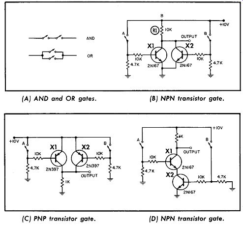
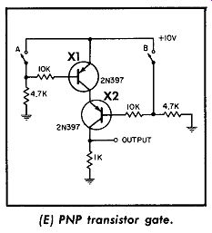
---------- Transistor logic.
(A) AND, and OR gates. (B)NPN transistor gate. (C) PNP transistor gate. (D) NPN transistor gate. (E) PNP transistor gate.
Circuits B and C show logic gates using parallel transistors.
The first uses NPN transistors. If closing a switch is an input, the circuit is an OR gate; if opening a switch is an input, it is an AND gate. Circuit C uses PNP transistors. If closing a switch is an in put, it is an AND gate; if opening a switch is an input, it is an OR gate.
Circuit C has the same input and output levels as B, but uses PNP rather than NPN transistors. If closing a switch is an input, both switches must be closed before the current through R1 ceases. Therefore, the inputs which make the NPN circuit an OR gate make the PNP circuit an AND gate. Because of this, the phase inversion inherent in transistor gates does not complicate the over-all circuitry.
The logic of circuits D and E are similar except the transistors are in series rather than in parallel. This change converts OR gates into AND gates and vice versa. Circuit D is a gate using NPN transistors. If closing a switch is an input, it is an AND gate; if opening a switch is an input, it is an OR gate. Circuit E shows a gate using PNP transistors. If closing a switch is an input, it is an OR gate; if opening a switch is an input, it is an AND gate.
PNPN TRIGISTOR SHIFT REGISTER
The basic circuit shown in Part A represents a one-bit memory element. It can be connected in cascade with identical circuits to form a complete shift register of as many bits as desired. A five-bit shift register is shown in Part B. The output pulse of the basic circuit may be either positive or negative, depending on whether the Trigistor was previously in an "on" or "off" state. Memory is achieved through the use of coupling diodes D1 and D2 and transition memory capacitor C1.
If the Trigistor has been off, the capacitor charges to 10 volts ( same as the supply). When shift pulse inputs are applied with polarities and references as shown, D2 will conduct and couple the negative pulse to the output. D1 remains reverse-biased and the positive pulse is blocked.
If the Trigistor has been on, its memory capacitor is not charged. Thus, when the two shift pulses are applied, D1 con ducts and couples the positive pulse to the output. D2 remains reverse-biased and the negative pulse is blocked.
A series of memory circuits, as in B, produces a shift register.
When a pulse input is applied to the base of X1, the shift pulses will propagate the signal down the chain.
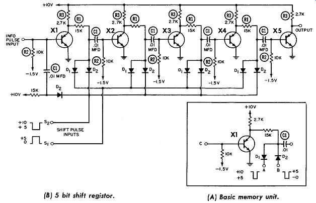
-------- (B) 5 bit shift register. (A) Basic memory unit.
PNPN TRIGISTOR AS A STATIC SWITCH
Two circuits using the PNPN Trigistor as a static switching device are shown in this diagram. The Trigistor acts as both a low-level logic element and a high-level static switch.
Once the Trigistor has been turned on, it will carry whatever current the load requires ( within its power-dissipation ratings). As an example, loads such as print hammers, solenoids, magnetic clutches, brakes, and relays are usually well within the current handling capability of the Trigistor.
As shown, this circuit has two separate loads. Assuming that diode D1 and the high-power load are disconnected, the rest of the circuit could be used as a portion of a logic circuit, such as a shift register or binary counter stage. When the Trigistor is on, the collector current through R1 is 4 ma. Applying a negative pulse to the base turns the Trigistor off, at which time the collector voltage rises to the supply-voltage level.
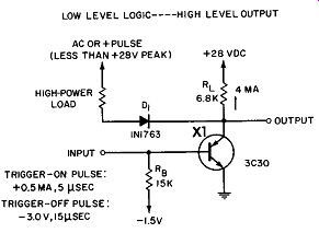
--------- PNPN Trigistor as a static switch.
With the diode and high-power load connected as shown, D1 will block the negative swings of AC voltage. The Trigistor collector current cannot exceed 4 ma at this time, so the Trigistor can be turned on and off as a logic-circuit element.
When the Trigistor is off, its collector will be at the positive DC supply level. Thus, when the AC voltage begins to go positive, D1 will continue to block (provided the DC supply voltage is greater than the peak positive AC voltage). But if the Trigistor happens to be on as a result of logic operations, collector current will be supplied to the high-power load through D1 during positive AC peaks. During this period of high current flow, the Trigistor cannot be turned off, so the logic and high-level output functions must be accomplished on a time-sharing basis. During each negative excursion of the AC voltage, one or hundreds of logic operations can be performed.
At the conclusion of a sequence of logic operations, "readout" is obtained by applying a positive voltage pulse to the bus connected to the power loads. Pulse power can be used, instead of AC, to operate high-power loads well up into the ampere region.
15-mhz PULSE GENERATOR
This circuit uses 2N501 transistors to form a pulse generator capable of operating from 50 khz to above 15 me. Capacitor C1 is adjusted for optimum output-pulse shape. Pulse width is deter mined by the input amplitude and the setting of resistor R1.
Variation of the output amplitude can be obtained by returning the collector of X3 to a variable supply voltage.
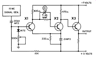
------------ 15 -mhz pulse generator.
COMMON LOGIC CIRCUITS
Many transistors readily meet the steady-state requirements necessary for logic circuits. Shown here are six common transistor logic circuits. Part A illustrates a resistor-transistor type in which the logic is performed by resistors. Any positive input produces an inverted output, irrespective of the other inputs. All logical operations can be performed with only this straightforward circuit.
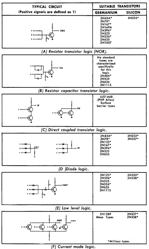
------------ Common logic circuits.
(A) Resistor transistor logic (NOR).
No standard types are characterized specifically for this logic
(B)Resistor capacitor transistor logic.
(PNP Alloy)
Surface barrier types (C) Direct coupled transistor logic.
(D )Diode logic.
(E) Low level logic.
(F) Current mode logic.
Part B is similar except that capacitors are used to enhance the switching speed. The capacitors provide a more rapid change in base current for faster collector-current turn-on. This type of circuit is faster than the RTL, but at the expense of additional components and stringent stored-charge requirements.
In Part C the logic is performed by transistors only. VcE and VBE, measured with the transistor in saturation, define the two logic levels. To insure stability and circuit flexibility, VcE must be much lower than VBE. Low supply voltages may be used to achieve high-power efficiency and miniaturization.
In Part D the logic is performed by diodes, and the output is not inverted. Amplifiers are required between the gate circuits in series to maintain the correct logic levels. However, several gates may be used between amplifiers, thus attaining high-speed operation. In this circuit, the non-inversion feature simplifies circuit design, and the components are relatively inexpensive.
Part E shows a low-level logic circuit using diodes. The circuit output is inverted. Diode D isolates the transistor from the gate, permitting R to turn on the collector current. By proper choice of components, the transistor voltage changes can be made very small. The number of inputs to the diode gate does not affect the transistor base current, thus providing more stable circuit operation. The small voltage changes minimize the effects of stray capacitance and enhance the switching speed.
Part F shows a current-mode logic circuit, where the logic is performed by transistors biased from constant-current sources to keep them far out of saturation. Both inverted and noninverted outputs are available, depending on which input transistor is pulsed. Very high switching speeds are possible because the transistors are operated under optimum operating conditions.
Although the voltage excursions are small, the circuitry is relatively unaffected by noise.
(A) Triggered pulse generator. (B) Frequency divider generator.
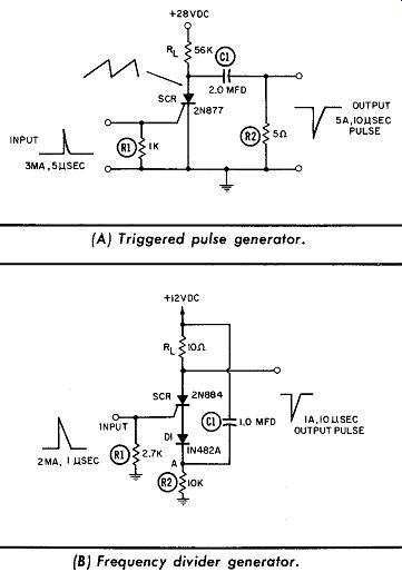
------------- SCR pulse and sweep circuits.
SCR PULSE AND SWEEP CIRCUITS
High-power pulses can easily be obtained from the high-sensitivity SCR. Outputs of 150 volts at up to 20 amperes can be produced from inputs in the 20-microampere and 0.6-volt ranges.
A power gain of 10,000,000 can be achieved in some cases.
A triggered RC pulse generator is shown in Part A. In its quiescent state, the capacitor is charged to the value of the sup ply voltage. When a trigger pulse is applied to the input, the CS fires, discharging the capacitor through the output load. This circuit can be triggered at any desired rate, and the output-pulse amplitude will be a function of that rate. The available output current is limited by the load resistor. A positive pulse output can be obtained by placing this resistor in the cathode leg and connecting the capacitor between anode and ground.
Circuit B shows another type of pulse generator, which is useful as a frequency divider as well as a pulse generator. Frequency division to 1/10 is possible. The charging resistor R2 is in the cathode circuit, and load resistor R1 is in the anode circuit. With no charge on the capacitor, the full supply voltage appears across R2. This provides a large negative bias between the gate and the cathode. Diode D1 is reverse-biased, preventing the gate-to cathode voltage rating of the CS from being exceeded. As the capacitor charges, the voltage across R2 decreases toward zero.
The CS will fire when the voltage at point A equals the gate firing voltage of the CS plus the forward drop of D1 ( approximately 1 volt total). Suppose the input-pulse amplitude is +2.5 volts between gate and ground, and the input-pulse rate is 20 khz with a supply voltage of 20 volts. If the time for the voltage at A to reach + 1.5 volts is 500 microseconds, then one output pulse will occur for each 10 input pulses. The output rate will be 2 khz, giving a frequency division of 10.
In RC pulse circuits which operate from a DC source and re quire the CS to turn off after each pulse output, C1 must be large enough to prevent the steady-state current through the CS from exceeding the dropout value. An upper limit also exists for R2; it must supply enough current to permit the CS to fire. The requirement for a minimum value of R2 does not apply to circuits turned off by other methods.
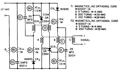
----------- AC static switching circuit.
T1 MAGNETICS, INC ORTHONOL CORE
#50007-IA A 5 TURNS-# 14 AWG B 200 TURNS-#28 AWG C 100 TURNS-tt28AWG T2: MAGNETICS, INC ORTHONOL CORE
#50007-IA A 5TURNS-#14AWG B 200 TURNS-,<2BAWG
AC STATIC SWITCHING CIRCUIT
This circuit utilizes the characteristics of square-loop core materials and SCR devices. Two small toroidal cores are used, together with two back-to-back stages (Types C-l0H or C-35H). This is directly analogous to a single-pole electromechanical con tractor with an electrically isolated solenoid. It is also possible, with slight modification, to make an analogy to an electromechanical latching relay.
Both SCR stages will fire when they receive a gate signal, and will thereby supply full-wave AC to the load. They will also act as the closed contacts of a relay or contractor. If no gate signal is supplied, no power will be supplied to the load.
There are two core transformers. T1 has three windings ( A, B, and C), while T2 has two windings as shown. During the "open" state, both cores T1 and T2 are saturated, Rectified current from the AC supply flows through the B windings and the diode rectifiers during alternate halves of the cycle.
When open, the gate voltage applied to the SCR's is limited to less than 0.25 volt by the voltage division across R1-R3 and R2-R4. The SCR's do not fire and no current flows in any of the reset windings.
A low-voltage signal, applied to input winding C, will fire the SCR, because the core of T1 will reset when the anode of SCR-1 goes negative. At this time CR1 is nonconducting. As the SCR anode begins to go positive, current will How through winding B of the transformer. C1 will charge through R1 Core T1 will saturate after about 1 or 2 milliseconds, discharging C1 through the gate of SCR-1 and causing it to conduct. Current will then How from the line, through SCR-1, to the load.
Gate firing for SCR-2 is the same as for SCR-1, but no separate signal winding is used. Core T1 depends on current through winding A to reset the core and allow SCR-2 to fire.
If SCR-1 is fired by the above sequence, its anode current will reset TL SCR-2 will fire on the following half-cycle, and full-wave current will be delivered to the load.
T1 will in turn be reset by the current through SCR-2. Hence, once SCR-1 begins conducting (initiated by a positive pulse on the signal winding of T1), the switch will remain closed even though a signal is no longer applied to the input.
The switch may be turned off by a negative pulse on the signal winding of T1 and thereby prevent winding A from resetting TL SCR-1 will then not fire on the following half-cycle, since the interruption of load current stops the reset action on T2. As a result, the circuit will revert to its "open" state.
The circuit acts like a latching relay, which is closed by a current How and then held closed by a mechanical latch. Once this circuit has been turned on, it will stay on, even though the main voltage is interrupted for long periods of time. In other words, this circuit "remembers" its last state as open or closed, even throughout power interruptions. Reset action requires a minimum load current of one ampere with the circuit closed.
Shorting out winding A on T1 is a modification of the circuit.
When this is done, load current will not reset T1, and a continuous positive DC signal must be applied to winding C of T1 to keep the contractor closed. The contractor will open within one cycle after this DC signal has been removed. Sensitivity of the switch to a control signal can be improved by increasing the number of turns on the C winding. C3 and R5 form a filter to prevent line-voltage transients from triggering the switch.
DIODE AND CIRCUIT
In this diode AND circuit, both anodes return to + 12 volts through 1,000 ohms. With no input to either diode, both are in the conductive state. The output voltage is nearly zero, since most of the drop is across the 1,000 ohms.
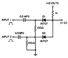
------------ Diode AND circuit.
A high positive pulse applied to the input of D1 will turn it off, but D2 will continue to conduct and there will be no output.
High inputs to both diodes will turn both of them off, and the output will be high. Hence, an output is obtained from both diodes; neither is capable of producing an output by itself.
DIODE OR CIRCUIT
All cathodes in this diode OR circuit are returned to -12 volts; thus, the diodes conduct with no input. If a positive input is applied to the anode of one diode, its low forward resistance will place the cathode voltage at about +5 volts. This +5 volts is the output; because it is positive and appears on the other cathode, the other diode will be blocked unless it receives a positive input pulse greater than 5 volts.
Thus, with a positive input at either diode, an output will be obtained.
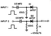
-------- Diode OR circuit.
VOLTAGE-LIMITING SCR DETECTORS
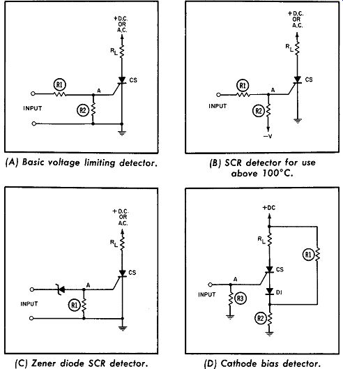
------------- Voltage-limiting SCR detectors.
(A) Basic voltage limiting detector. (B) SCR detector for use above 100°C.
(C) Zener diode SCR detector. (D) Cathode bias detector.
Their properties make the CS and SCR particularly useful as voltage-limiting detectors and other voltage or current threshold circuits. The high-sensitivity series, with a maximum gate firing current of 20 microamps and approximately 0.5-volt gate firing voltage, has been designed for this type of application.
The threshold firing point can be set at any desired value, from 0.6 volt up, by the use of an input voltage divider or zener diodes.
Voltage-limiting detectors can use either DC or AC load power.
If DC is used, the CS will latch when the input exceeds the threshold voltage. If AC load power is used, the CS will supply power to the load only when the input voltage exceeds the threshold voltage. Voltage-limiting detectors using the CS are quite simple and useful in a variety of timing, sensing, indicator, warning, and safety applications. Since the CS can handle high load power, it can directly actuate the controlled circuit in many cases. A low power input from pressure, temperature, speed, flow, light, or similar transducers can be made to turn on the CS at a preset level. The CS can then actuate a control circuit, relay, solenoid, buzzer, indicator light, horn, or other output.
A basic form of voltage-limiting detector is shown in circuit A. Its operation is based on the fact that the CS will not turn on until the minimum gate firing voltage is exceeded. The ratio between R1 and R2 determines the threshold firing voltage at the input. The firing voltage of the CS has a negative tempera ture coefficient of approximately 3 millivolts per degree C. Compensation will be necessary if a uniform firing voltage is to be used over a wide operating-temperature range.
The value of R2 is determined by the required bias-off current at the upper operating temperature, to insure a stable "off" condition for the CS. Circuit B is for operation at temperatures above 100°C. With a negative bias supply, R2 can be larger than when returned directly to the cathode. A larger value will also reduce current loading on the input.
A zener diode can be used to set the input threshold as shown in Part C, where a higher input voltage and minimum loading are desired. A zener diode with a positive temperature coefficient can be used to compensate for the negative coefficient of the CS. A further degree of refinement could be achieved by using a negative temperature-coefficient resistance for R2, to compensate for changes in firing current with temperature. Thermistors work very well for this purpose. Another arrangement, which uses positive cathode bias, is shown in Part D.
THE SCR AS AN AC STATIC SWITCH
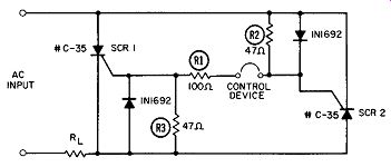
----- SCR's as AC static switch.
SCR's can be used to control the amount of AC power applied to a load. In this circuit, C-35 rectifiers are connected in inverse parallel and conduct during opposite alternations. The SCR's act only to control the AC; they do not act as rectifiers.
The control signal which permits each gate to fire may be from an electronic control amplifier actuated by light, heat, pressure, etc. When the control device closes, the SCR' s fire once for each alternation. When the switch is open, neither SCR fires. In this way, AC power to the load is controlled. C-35 SCR's are shown, where R1 is 100 ohms and the input is 117 volts. Other parts values may be used for different input voltages.
TUNNEL-DIODE BISTABLE CIRCUIT
Tunnel diodes are fast and effective switches. A simple bistable circuit or flip-flop is shown here. The tunnel diode is biased to the low-voltage state by a current which is slightly lower than the peak current. Since the transistor is off, the collector is at the supply voltage.
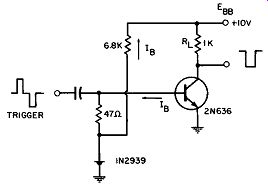
------------ Tunnel-diode Bistable circuit.
If a positive trigger pulse supplied at the input is such that the tunnel-diode current exceeds the peak current, the tunnel diode will switch to its high-voltage state. It will remain in this state, with most of the bias current being diverted into the base, until a negative trigger returns the diode to its original low voltage state.