AMAZON multi-meters discounts AMAZON oscilloscope discounts
OUR introduction to the transistor in the last section was a bit formal, but now that the strangeness has worn off, we see that the transistor is just the application of some well-tested ideas but using a new technique. We have input and output circuits, just as with tubes. Our input is the base-emitter circuit, with the emitter (for the n-p-n transistor) analogous to a cathode, and the base to a control grid. And, just as in the case of a tube, the input signal varies the bias. The output is the collector-emitter circuit, with the collector ( again, for the n-p-n type) reminiscent of the plate in a tube. (See Fig. 401-A,-B.)

Fig. 401. The voltage between emitter and collector is the sum of the
battery voltages of both p-n-p and n-p-n circuits shown here. Although
the circuits have been drawn somewhat differently than those in Section
3, if you will examine the circuits you will see that all biasing requirements
have been met.
Because you may be much more familiar with tubes than you are with transistors, the temptation to make comparisons between them will always be with you. In a way this will be unavoidable since many of our old, familiar tube circuits have been picked up, lock, stock and resistor, and simply put to use with transistors ... with some component changes. However, we just cannot pull a tube out of a circuit with the idea of substituting a transistor -- and then sit back and hope for the best. If we do, the best will never arrive. A transistor has characteristics of its own.
Biasing methods
Transistors are much simpler than tubes in their voltage requirements. All that the triode transistor needs is a forward bias for its base-emitter circuit and reverse bias for its collector-emitter circuit.
Fig. 401 shows one possible arrangement for bias for a p-n-p and an n-p-n transistor. The voltage between collector and emitter is the sum of the voltages of B1 and B2 just as it was in the circuits you saw in the last section. In the new arrangement of Fig. 401, though, both the input and output circuits share the voltage of B1. We can re-arrange the batteries as shown in Fig. 402 so that each circuit--input and output--has its own bias supply.

Fig. 402. In these circuit arrangements, the bias voltages are independent
of each other, but now battery B1 does not add to the voltage between
emitter and collector.
However, in Fig. 402, the voltage between collector and emitter is now reduced by the amount of BI. We can overcome this by increasing the value of B2. The disadvantage of the circuit of Fig. 401 is that we cannot change the forward bias without, at the same time, changing the reverse bias. The arrangement in Fig. 402 eliminates this difficulty, but we do lose the advantage of the added voltage supplied by the series connection of Fig. 401.
Single battery operation
We can eliminate one of the batteries altogether, as shown in Fig. 403. Note that in this n-p-n circuit, the collector is still positive with respect to the emitter, while the base is also positive.
Thus, we meet the conditions for biasing this transistor. Now it might seem odd that we can do this, since the input and output circuits require different amounts of biasing voltage. But you will note that R1 is in series with the battery in the base-emitter circuit while R2 is in series with the same battery in the collector emitter circuit. By selecting the right values for R1 and R2, we can still have the voltages we want. This might seem to give us the flexibility of the circuit of Fig. 402--and so it does--but remember that we pay for it by having voltage drops across R1 and R2.
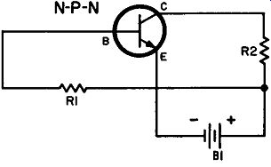
Fig. 403. A single battery, B1, supplies both forward and reverse bias.
The correct amounts of bias can be obtained by selecting the proper values
for R1 and R2.
Fixed bias
Although the circuits of Fig. 401, 402 and 403 are different, they do have one item in common. The forward bias has a fixed value, the amount of bias being determined by the voltage of the forward biasing battery (B 1) and the value of R 1. In these circuits, to change the forward bias we would generally use a different battery. For a particular value of base bias, the bias current remains constant. Fixed bias has the serious disadvantage that it is best for one particular operating point or set of conditions only. There are two factors that make life difficult for fixed bias.
Transistors are temperature-sensitive. This means that the operating characteristics of a transistor will change with temperature.
Also, there is quite a bit of variation, even between transistors of the same type number, so that if you replace a transistor (in a circuit having fixed bias) you cannot be sure that the bias is correct. To make it correct, you would need to experiment with B1, or R1, or both.
Self bias
We can make the bias self-adjusting (which is why we call it self bias) as shown in Fig. 404. The circuit is exactly the same as that shown in Fig. 403, with but one change. In both cases, one end of R1 is connected to the base. The other end of R1, though, (in Fig. 404) is wired to the top end of R2. Now let's see how this changes the circuit from fixed to self bias. First, using Fig. 403 as our guide, let's trace the path of the base-emitter circuit. Starting at the emitter, we go through the transistor to the base, from there through R1, then through battery B1, and so back to the emitter. But if we try to follow the same path in Fig. 404, we now find that we must include the collector load resistor R2, in our path. What difference can this possibly make?
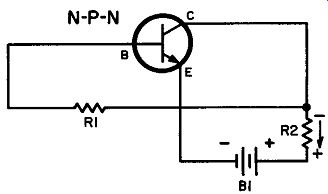
Fig. 404. In this circuit, forward biasing depends on the amount of
collector current flowing through R2.
In Fig. 404 we have an arrow immediately next to R2. This arrow shows the direction of current flow and the polarity of the voltage drop, across R2, due to collector current. This voltage is in opposition to the battery voltage. But the voltage between the base and the emitter (our forward bias) depends almost entirely on the arithmetic sum of these two voltages--the battery voltage and the drop across R2. If collector current is large, so is the voltage across R2. A large voltage across R2, though, means less for ward bias. If forward bias decreases, less current passes through the transistor and so collector current decreases. This reduces the drop across R2. Less voltage across R2 means more forward bias.
Sometimes the act of drawing a circuit hides the information it is supposed to convey. Generally, most circuits are prepared so that there is an orderly progression of signal, from left to right.
This means that we start with a weak signal at the input, moving through circuit after circuit, toward a strong signal at the output.
In a way this makes sense since we then try to "read" the circuit just as though we were trying to read a line. Its disadvantage is that the circuit becomes less clear electronically.
To understand what this is all about, take another look at Fig. 404. To understand what is happening in the way of forward biasing, you would need to trace the entire circuit between the input elements--the base and the emitter in this case. While this might be fairly easy to do in the case of Fig. 404, remember that what we are dealing with here is a very simple circuit. It might not be so simple when associated with a half-dozen or more transistors and assorted parts.
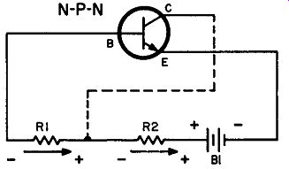
Fig. 405. This is not the way in which we usually draw a transistor
circuit, but it does show forward biasing very clearly.
To see just what is happening in the way of bias, examine Fig. 405. Here we have redrawn Fig. 404 in a somewhat unorthodox manner so that you can see what is happening quite clearly. Let's trace the paths of current flow, beginning at the negative terminal of B1. From here we move into the transistor, through the emitter and base, through R1 and R2, and back to the battery once again.
The arrows across R1 and R2 show the direction of electron flow and because we know this direction, we know the polarity of the voltage drops across R1 and R2. These voltage drops are in opposition to the battery voltage. And what is the voltage between emitter and base--in other words, what is the amount of forward bias? It is equal to the voltage supplied by battery B1 minus the voltage drops across the· two resistors--R1 and R2.
Now let's consider R1 and R2. Because we have drawn them with equal physical dimensions, we might succumb to the temptation to regard them as having equal voltage drops. There are several reasons why this is most definitely not so. First, consider the relative resistances of R1 and R2. R1 has a very small value, much smaller than that of R2. But there is another important consideration. Examine the dashed line we have drawn from the collector to the junction of the two resistors. This represents an other path of current flow--a path that does not include R1. Furthermore, just to make the evidence more compelling, this current is many times greater than the current flowing through R1. All in all, the voltage drop across R2 is much greater than that across R 1 and for this reason is the determining factor in the forward biasing of the transistor.
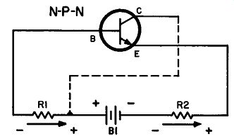
Fig. 406. Although B1 and R2 have been transposed (see Fig. 405), circuit
operation remains exactly the same.
One other fact emerges from a study of Fig. 405. We can trans pose R2 and B1 without affecting the circuit. When we do this the amount of current flow through R1 and R2 is not changed.
If you will examine Fig. 406 you will see that the status of the components and their behavior has not been altered. But if you will now move along to Fig. 407, you might very well imagine that we have a completely new circuit. Actually, it is not new in the slightest. It is identical with that of Fig. 404. The difference (as in the case of Figs. 405 and 406) is in the transposition of B1 and R2, a change that does not affect operation of the circuit.
We've had a rather steady diet of resistors in the output, so suppose we insert a coil, L1, as shown in Fig. 408. But because we want variety, we have given ourselves a problem. We had depended on the resistance of the load to give us a voltage drop.
Our coil, though, isn't so obliging. We can solve this difficulty quite easily by inserting a resistor, R2, in the emitter circuit.
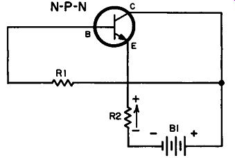
Fig. 407. This circuit is identical with that of Fig. 404. Transposition
of B1 and R2 has not changed circuit operation.
Fig. 408. In this circuit, coil L1 is used instead of a load resistor. This coil could be the primary of a transformer.
This resistor performs exactly in the same way (as far as forward bias is concerned) as load resistor R2 in Fig. 404. The arrow alongside R2 gives us the direction of electron current flow and also the polarity of the voltage drop across R2. Again, this voltage is in opposition to the battery voltage. If you will take a walk, starting at the emitter, through the transistor to the base, you will see that we can continue through R1, the battery, and then R2.
The position of the resistor hasn't changed the fact that we still have self bias.
Collector voltage vs collector current
To learn the condition of a patient, a doctor pokes, probes, listens with his stethoscope, and finally gets a picture of the patient's general state of health. We follow a similar routine with transistors, except that our equipment consists of a microammeter (to measure base current) and a milliammeter (to measure collector current) as shown in Fig. 409. While this setup is for an n-p-n transistor, the same arrangement (with transposed batteries) would do for a p-n-p.
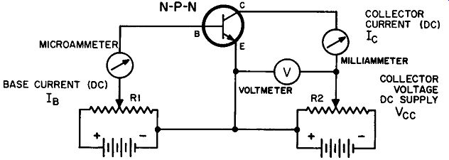
Fig. 409. Setup for determining the relationship between collector voltage
and collector current.
Collector characteristic curve
With the test circuit of Fig. 409 we can obtain a relationship between collector voltage and collector current. This is a static test. All that this means is that we are going to apply de voltages only. You might think that this isn't quite fair, since our transistor is ultimately going to work with a signal input, yet the collector characteristic is important. We've been talking aboutputting bias voltages on our transistor, and have examined several circuits.
The collector characteristic is going to help us come to a decision on just what values of bias we should use and what sort of a resistor we should have as our collector load.
Fig. 410 shows the results of one test using the circuit of Fig. 409. R2 was set f-or different values of collector voltage. R1 was adjusted to keep the base current at a constant 40 microamperes.
Now examine the curve between the points at which we have 2 volts on the collector, and 6 volts. At 2 volts, the collector current is slightly less than 5 ma. At 6 volts it is slightly above 5 ma.
This is quite a range of collector voltage change, and yet the collector current has remained substantially constant, with a constant amount of base current.
If we were testing a tube, we would be measuring plate voltage vs plate current, for a particular value of grid bias and in this way we would obtain a plate characteristic curve. In Fig. 409 we measured collector voltage vs collector current for a fixed amount of bias current, and obtained a collector characteristic curve.
Thus, base current in the transistor performs the same function as grid bias voltage in a tube.
Tube vs transistor biasing
There is, of course, a mental hazard in equating vacuum-tube grid bias and the technique we use for forward-biasing a transistor.
In the vacuum tube, an increase in bias means that we are making the control grid more negative with respect to the cathode. As far as bias is concerned, we are moving in a negative direction and the result is a decrease in plate current. In the case of the transistor, the base is biased either negative or positive with respect to the emitter, depending on whether we are using a p-n-p or n-p-n type. Furthermore, an increase in bias, regardless of the transistor type, means an increase in collector current, an action quite opposite to the plate current decrease resulting from raising the bias in a vacuum tube.
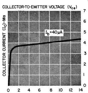
Fig. 410. Collector characteristic curve. Note how little the collector
current changes with collector voltage for a given value of base current.
Collector characteristic family
A single collector characteristic, such as that shown in Fig. 410, supplies limited information. To learn more about the transistor, we can have a whole family of collector characteristics, as in Fig. 411. The procedure for obtaining these curves is exactly the same as that outlined earlier. In this we get a whole family of curves, all the way from zero base current, in steps of 10 microamperes, up to 60 microamperes. Note how similar the collector characteristic curves are to the plate characteristics for a 6AK6 pentode, shown in Fig 412. The curves are similar, yet the transistor we have been testing is a triode. The straight line portion of the curve, (whether tube or transistor) is the useful part. In the transistor, we get to the straight line portion quite rapidly. In Fig. 411, all we need is about one quarter to one half volt. For the tube, we need about 7 5 volts on the plate before we get the same results.
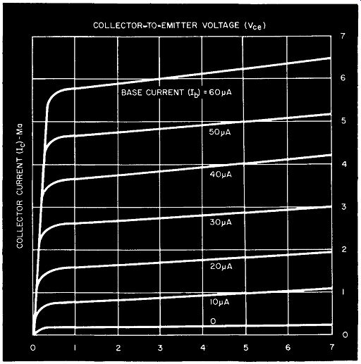
Fig. 411. Family of characteristic curves for a transistor.
This gives us another clue to transistor vs tube behavior. Transistors not only work with smaller voltages than tubes, but respond to much smaller variations in voltage. If you're accustomed to tube potentials, revise your thinking downward for transistors.
The collector load
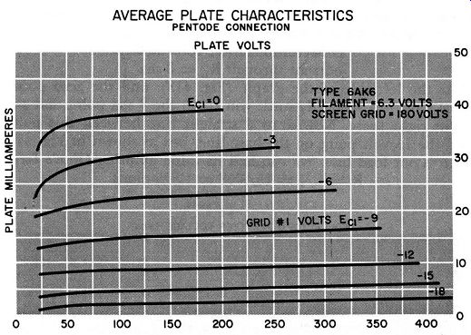
Fig. 412. Pentode characteristic curves. These are similar to characteristic
curves far a transistor. The transistor, though, is a triode while the
curves shown here are for a pentode tube.
In a transistor circuit (as in a tube circuit) the components must work together as a team. It takes just one wrong part or value to make the circuit act sluggishly, or not at all. This doesn't mean that there is only one right combination of parts and values--there are many. The whole idea is to select the one right group out of the many available.
At first thought this might seem like an impossible suggestion, since the number of variables involved would give us a very large number of component combinations. That is why characteristic curves of transistors--and of tubes--are so important. They give us some idea about the behavior of these components and enable us to make a selection of associated parts in a more intelligent manner.
To see how this concept works, start with Fig. 413 which gives the collector characteristics for a transistor. Since the collector-to emitter voltage ranges from zero to 20, let's start with a battery of 15 volts, using the circuit shown in Fig. 414. Why 15 volts? It is just a starting point, and possibly not the best one either.
Using the circuit of Fig. 414, suppose we connect a wire between the collector and emitter. Since this is a short across these two elements of the transistor, the collector to emitter voltage be comes zero. The full voltage of the battery is now across the load resistor, RL. The amount of current will now depend only on the battery voltage and the value of RL. Suppose this current is 8 milliamperes. We now have a condition of:
collector-to-emitter volts = 0
current through RL = 8 ma
At the left side of the graph (Fig. 413) find the zero point.
Now move up vertically until you reach the 8 ma point and put a dot right there. Now draw a straight line between this point and the 15 volt point on the base line, just as shown in Fig. 413.
This is our load line. We can find its value by using Ohm's Law:
R = E/I = 15/.008 = 1,875 ohms
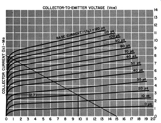
Fig. 413. Family of collector characteristics.
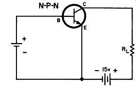
Fig. 414. Simple circuit used for measuring collector characteristics.
The value of forward bias can be changed to obtain the base current values
shown in Fig. 413.
We cannot dismiss the graph in Fig. 413 now because it contains information we need. Let's move along, first, to the 15-volt point on the base line. What is this 15 volts? We know it is our full battery voltage, but there is more to it than just that. The description on our base line tells us that we are working with collector-to-emitter voltage--that is, the voltage existing between the collector and the emitter. But for a full 15 volts to exist between collector and emitter, we cannot afford any voltage drop across RL. We can eliminate the drop across RL in two ways. We can assume the transistor is at cutoff--that is, no collector current flowing, or else we can put a shorting wire right across RL. Whichever method we use, the voltage between collector and emitter would be the full battery voltage.
However, we did put the load resistor in the circuit for a purpose--to develop an output signal across it, so now let us remove the short from across RL or else take the transistor out of cutoff.
If collector current flows at this time, it will also pass through RL, producing a voltage drop across it. This means we will now have less voltage between collector and emitter. Thus, if we have a 5-volt drop across RL we will have:
15 - 5 = 10 volts between collector and emitter
At this time, how much current is flowing in the output circuit? Move your finger along the base line until you reach the IO-volt point. Now move straight up until you reach the load line. Then move across horizontally, toward the left, until you reach the vertical current line. The intercept is at 2.7 milliamperes.
What do we learn from this? As the voltage between collector and emitter becomes smaller, current in the output circuit gets larger. Carrying this to its logical conclusion, our graph shows us that when the voltage between collector and emitter becomes zero, we have a maximum current of 8 ma flowing through the load.
We need only two points to determine the load line. We used two extreme conditions:--I) a condition of maximum current (8 ma) and zero collector-to-emitter voltage and 2) a condition of maximum voltage (15 volts) and zero current in the output circuit.
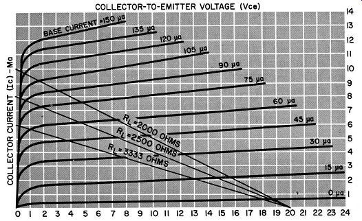
Fig. 415. When the load line intersects base-current curves that are
equally spaced, distortion produced by the transistor will be at a minimum.
A little earlier we found the value of the load line by using maximum values, but this value is confirmed even when current is flowing through both transistor and its load. In Fig. 413 we see that for a 5-volt drop across the load, we have 10 volts remaining between collector and emitter. For this value of voltage, we get a current of 2.7 ma. The load value then is:
5 volts .0027 ampere 1,852 ohms
Obviously, the value of the load is equal to the voltage across it divided by the current through it. The graph in Fig. 413 gives us this information. The voltage across the load is equal to the battery voltage minus the drop between collector and emitter.
Other values of load The slope of our load line depends on the battery voltage and the current that flows in the circuit with the collector-emitter shorted. The slope becomes steeper for different values of load as shown in Fig. 415.
We can use load lines to see which one will give us the least amount of distortion. Suppose we assume that we are going to start with a base current of 45 microamperes. We will then de crease our forward bias, dropping the base current to 30 micro-amperes, and then increase it to 60 microamperes; that is, we will decrease and increase our base current by 15 microamperes. When we do, and tabulate our results, this is what we will get:
When RL = 3,333 ohms
When RL = 2,500 ohms
When RL = 2,000 ohms
Since we get almost equal swings of collector current for equal changes of base current, distortion in the output will be small.
Note that our operating point (sometimes called the quiescent or Q point) is at the intersection of the load line and the base current curve.
How do we know that we won't get distortion? Look at the base current curves. They are fairly equally spaced. This means that an increase or decrease of base current will produce fairly equal changes in collector current. If the base current lines were not equally spaced, we would not get equal changes in collector current for equal changes in base current. You can see an example of this sad situation in Fig. 416. Our operating point is at the intersection of the load line with the curve for a base current of 200 microamperes. Our input signal has a peak-to-peak value of 200 microamperes--that is, it has a positive component of 100 microamperes and a negative component of the same amount.
Our base current, then, is going to swing 100 microamperes either way. Note the uneven spacing of the base current curves. The distance from our starting point to the 300 microampere curve is much smaller than the distance from the starting point to the 100 microampere curve. This means that our collector current variation is not going to be symmetrical. Our input signal current, though, is symmetrical. What the graph is trying to tell us is that our transistor is going to distort the signal.
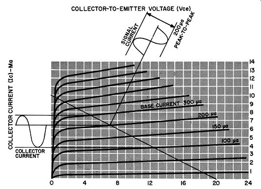
Fig. 416. Distortion will result because of the unequal spacing of the
base current curves above and below the quiescent point.
How serious is the situation in Fig. 416? The collector current waveform doesn't look too different than the signal current wave form. The answer here is that the amplitudes of the two wave forms mean little until we consider that the signal current is in microamperes and the output or collector current is in milliamperes. A milliampere is a thousand microamperes. Viewed in this light, if we consider the signal current as "same size", then the collector current waveform is a thousand times larger. Does this mean that the gain of our transistor is a thousand? Hardly! The variation in output voltage is still the product of the collector current multiplied by the value of the resistance through which it flows.
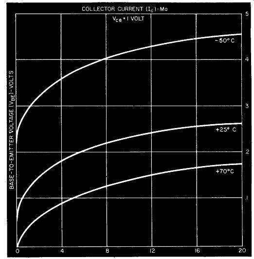
Fig. 417. Transfer characteristic curves. These graphs show the effect
of temperature on collector current.
Mutual or transfer characteristics
The graph in Fig. 416 is a bit of scientific fortune-telling. With its help, we can begin to predict just how the transistor will behave and what we can expect from it. But you can't expect a transistor to reveal all in just one picture, so, just to be able to say that we are more than just nodding acquaintances, let's work with a new graph of transistor characteristics--the one shown in Fig. 417.
In Fig. 417 we have plotted (sounds sinister, but it isn't) base to-emitter voltage vs collector current. But what is base-to-emitter voltage? Just our old friend, forward bias. And, as the curves show, as our forward bias goes up, so does our collector current.
There are a few exciting facts we can gather here. Take a look at the lowest curve--the one marked 70°C. When the forward bias is zero, so is the collector current. But as we increase the forward bias--not by volts, mind you--but by tiny fractions of a volt--whoosh, away goes the collector current.
There's still another item that's just as important. As the temperature changes, so does the collector current. Actually, we should have had just one curve. Having the temperature affect the collector current isn't at all desirable. In Fig. 417 we have only three curves because the temperature changed only three times.
But what if the temperature kept going up and down. Which curve would be the right one? You can be sure we're going to do something about that, in just a few moments.
In the meantime, why should we consider a graph of the type in Fig. 417 so important? This graph gives us an insight into the amplifying properties of the transistor. We can see (we don't have to imagine) the effect of forward bias on the output or collector current. Curves of this sort are known as transfer or mutual characteristic curves.
Stabilization
Most tubes (there are some exceptions) operate at respectably high temperatures. Try removing a power tube (after it has been on for a few minutes) with your bare fingers, and you'll have a dramatic example of what we mean. Even low-voltage miniatures have a temperature much higher than that of the surrounding air. This means that tubes aren't affected by room temperature -
they have their own, warm operating region.
But transistors don't have heated filaments or cathodes. They don't have plates that must dissipate heat. It doesn't take much of a rise in temperature to set the electrons in a bit of n-type germanium to thinking about traveling over to those very attractive positive charges just on the other side of the potential barrier.
But in a transistor (or in a tube) it is we who must control the current, and not temperature, or any other nonsense of that sort.
You might think that we're making a big fuss over a small matter, but in Fig. 417 we went to the trouble to draw graphs of transistor behavior for you. Temperature changes mean that these curves vary all over the place. And if these curves change, then so will the current gain change, and naturally, right along with it, the output impedance will vary. This is definitely not a good situation.
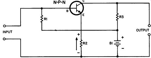
Fig. 418. R2, common to both input and output circuits, is a stabilizing
resistor.
We can "immunize" the transistor, protect it against the seductive effects of temperature by stabilizing it. One technique we can use, known as current feedback, is shown in Fig. 418. The circuit is similar to one we talked about earlier--Fig. 407. However, let's consider R2 from a new point of view.
R2 is in a rather unique position. Trace the output circuit and you will see that it is part of it. But you can do the same with the input circuit. R2, then, is common to both, and holding on to this tidbit of information in our hot little hands, we can learn of two ways in which R2 overcomes the effects of temperature.
Let us say that the temperature does change and in such a way that the collector current increases. What other change could have produced the same result? We could have increased the collector voltage or we could have increased the forward bias, or we could have done a little bit of both. But, as far as we know in this case, none of these things happened.
With an increase in temperature, our collector current starts to rise. The collector current not only flows through R3, but through R2 as well. Note the direction of current flow through R2. This produces a voltage drop across R2 whose polarity is such that the top end of R2 (the end connected to the emitter) is plus and the bottom end ( the end connected to the base through the signal input) is minus. Since our transistor is an n-p-n type, our forward bias works by putting a negative voltage on the emitter and a positive voltage on the base. The voltage across R2, though, acts as a reverse bias for the base-emitter circuit. Or, we could say that the forward bias is being opposed by the voltage across R2. Since, in effect, the forward bias is being reduced, the collector current decreases.
This isn't the only action that takes place. Collector current depends on the voltage existing between collector and emitter.
This voltage is supplied by the battery. The actual voltage between collector and emitter, though, isn't the full amount of battery voltage for we must subtract the amount of voltage dropped across load resistor R3. In addition, in the case of the circuit of Fig. 418, we must also subtract the voltage drop across R2.
Thus, R2 acts in two ways to counteract the increase in collector current caused by a rise in temperature. It reduces forward bias and it also reduces the collector-emitter voltage.
Current feedback
Components in some circuits often perform a dual function, but the name given to the component is often a concession to the more important function. Thus, a coupling capacitor is so called because it couples one stage to the next, but, at the same time, it is a blocking capacitor, preventing the de voltage of a previous stage from moving over into the following one.
In Fig. 418, R2 is a stabilizing resistor, but it does more than just that. Let us imagine that we now have an incoming signal.
If die signal (at a particular moment) increases the forward bias, collector current will increase. But this increase in collector current will produce more voltage across R2, which, of course, has a certain amount of opposition to the increase in forward bias.
Since the voltage across R2 will vary at the same rate as the input signal, but will oppose it, we can see that we have an out-of-phase condition, or, a form of negative feedback. And, since negative feedback reduces the gain of the stage, that is exactly the sort of result we can expect from R2. This type of negative feedback is called current feedback.
Negative feedback is a sensible way in which to stabilize a transistor against increases in current due to temperature rises. It's just like having too much water pouring out of a faucet. We don't telephone back to the reservoir and tell them to cut down on the pressure. All we do is turn the valve a bit.
Since negative feedback is the solution to our temperature problem, we can use any form of out-of-phase feedback (negative feedback) we want. Fig. 419 is an example of what we mean. Here we have an n-p-n transistor. As we make the base more positive (a positive-going signal can do that for us), collector current increases. This produces a voltage drop across R3. The arrow shows us that the top end of R3 is negative-going (it is becoming more negative with respect to its other end). All we need do now, is connect the negative-going end, through R4, to our positive-going base. This is a form of negative feedback, since the voltage R4 steals from R3 is out of phase with the input signal. We call this voltage feedback.
If you've examined the circuit of Fig. 419 carefully, you've probably observed that we still have R2 in the circuit. Shunted across R2 is an electrolytic capacitor. We could remove this capacitor, and then we would have both voltage feedback (supplied by R4) and current feedback (supplied by R2). Feedback of this sort not only keeps temperature changes at arm's length, but also improves the performance of the circuit. We're not going to discuss it further at this point, since we would be encroaching on the material in section 5.
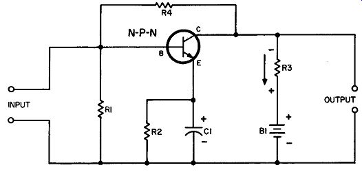
Fig. 419. We can immunize the transistor against the effects of temperature
by using voltage and current feedback.
Input resistance
Whenever we have voltage and current, we always have resistance. We may not even have a physical resistor in the circuit, but the fact that we can divide the voltage across a pair of points by the current flowing between those points, means that we must have resistance. And the movement of current is one of those facts of life we must always associate with the transistor. Whether or not we have a signal, we always have current flowing in both input and output circuits.
Resistance can be measured directly or indirectly. We can put the leads of an ohmmeter right across a resistor, and there you are--the value of resistance can be read directly from a scale on the meter. But if we have current flowing (whether or not we have an actual resistor in the circuit) we must put our ohmmeter away and measure resistance indirectly.
Fig. 420 shows how easy this is to do. Here we have a de micro ammeter connected between base and emitter. This will measure our base current. And, shunted across the base and the emitter we have a high-impedance vacuum-tube voltmeter to measure our voltage. Divide the voltage reading by the current reading and we have the input resistance.
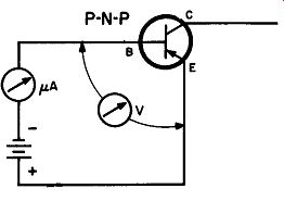
Fig. 420. Setup for measuring in put resistance.
In Fig. 420 the collector floats--that is, we have no provision for reverse bias. The collector-emitter is open circuited. Remember--a transistor is different from a tube in that there is no isolation between the elements. The emitter, base and collector are in close contact. Thus, in measuring the input resistance we want nothing in the collector circuit to affect our test.
What value of voltage shall we use in Fig. 420? We use the amount of forward bias voltage determined by the location of our operating point on the load line. This value is used since this is the value at which the transistor will operate.
Output resistance
In measuring output resistance, our input will now be open circuited, but the transistor will have its operating reverse bias applied, as shown in Fig. 421. And, while we are on the subject of input and output resistance, keep in mind that we can run the same tests on n-p-n units just as easily (Figs. 420 and 421 show p-n-p's). All we do is transpose everything--the leads to our test meters and the leads to our battery.

Fig. 421. Setup for measuring output resistance.
Small and large power
In a vacuum tube circuit, events move along very smoothly until we reach the speaker. Most speakers are current-operated devices. This means that the tube--or transistor--preceding the speaker must be a power type. All tubes preceding the output tube can be voltage amplifiers. Voltage amplification is their primary concern. But the output tube (because of the demands of the speaker) is interested in power--the product of volts and current.
Transistors are not excused from these requirements just be cause they are transistors. Unlike tubes, transistors are current operated devices--that is, current flows in both the input and output circuits of a transistor at all times. But how much current? For transistors preceding the output transistor, currents are measured in microamperes and milliamperes. The output transistor, though, like its tube counterpart, must be a power type. In its output circuit we will have current in the order of milliamperes or amperes.
Our transistor menu
One of the nicest parts about dining out is that you can get a menu and plan your own dinner. For your transistor menu we are going to serve transistor audio amplifiers in your next section.
Following that, we are going to move back, stage by stage (in the succeeding sections) until we have covered an entire receiver. And then, for your electronic dessert we will serve you with information on different transistor types and miscellaneous applications.
We hope your appetite for knowledge will keep up with what we are going to put before you.
QUIZ
1. What is meant by fixed bias?
2. What is self-bias? How does it differ from fixed bias?
3. Describe the circuit arrangement for determining the relation ship between collector voltage and collector current.
4. What is a static test?
5. Explain the method for determining the load line for a transistor.
6. How can load lines be used to determine possible distortion?
7. What is the quiescent point?
8. What is a mutual characteristic?
9. What is stabilization? Why is it needed? What is a stabilizing resistor?
10. What is current feedback? What are its effects on a circuit?
11. In general, what is the relationship of input and output resistance in an amplifier circuit?
12. Transistors are current-operated devices. What does this statement mean?