AMAZON multi-meters discounts AMAZON oscilloscope discounts
IT may seem very odd that we should have a section entitled Circuit Analysis. And we wouldn't be at all surprised if you were to demand, "And what have we been doing up to now? Studying medicine? Law? Business? True! Quite true! Take a single component such as a resistor, connect another component or a battery, and we have a circuit. We've been doing that almost from the very beginning of the guide. But what sort of circuits have you and we gone through together? Wouldn't you say that they've been the common-garden variety, the sort of stuff you would logically expect? We've had audio and rf amplifiers, converters, mixers and oscillators. And before that we had a generalized conglomeration, just so that we would get the idea of how transistors behave in the polite society of resistors, capacitors and batteries.
If we were to stop right there you would have every right to say, "So what? Is that all transistors can do?" Quite correctly you expect more, so let's examine some other transistor accomplishments.
Before we do, though, we are sure you know by now that a transistor isn't just a vacuum-tube substitute. We can't take a vacuum-tube circuit (remove Dr. de Forest's brainchild), put in a transistor, and then say, "There, that's that." Hardly! Transistors have their own ideas as to the components that should accompany them. Does this mean, then, that you are going to need to learn a whole line of new circuits and that your knowledge of vacuum tube circuits has gone down the drain? No--for you will see that the basic circuit idea has remained the same and in many cases you will be able to identify the circuit from earlier experience and knowledge. So let's start in an easy way and see what we can do together. However, please remember that this is not a construction section. The purpose here is to learn more about how transistor circuits work through theory analysis.
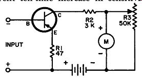
Fig. 801. Insensitive meter can be used to measure currents in the order
of micro amperes with the help of a transistor amplifier.
Meter amplifier
Of all de milli-ammeters ever manufactured, the one having a full-scale deflection of one milliampere (sensitivity, 1000 ohms-per volt) was probably the most common. At one time this meter was a workhorse but with improvements in magnets and manufacturing techniques, much more sensitive meters are being used.
The great big hitch here, of course, is that the more sensitive the meter, the more it costs. The circuit shown in Fig. 801 will give a meter an apparent ten-time increase in sensitivity, but by the time you get through paying for the parts, you may not have made any savings at all. But at least its nice to know that you have a choice.
To understand the circuit of Fig. 801, think of the current amplification capability of a transistor. In an earlier section we called this beta. It is the ratio of the change in collector current to a change in base current. For a representative transistor, beta could have a value, say, of 50. Thus, if we had 20 microamperes of base current, we would have 1,000 microamperes (or a milliampere) of collector current. And if the base current changes, we get 50 times as much change in the collector current.
Now suppose that in the circuit of Fig. 801 we had a de milliammeter in the base circuit of the transistor. We would need a very sensitive meter indeed to give us a full-scale deflection of 20 microamperes. But if we had a de meter in the collector circuit, we could easily use a 1 milliampere movement. We could calibrate this meter in microamperes and when it would read full scale we would be measuring a current of only 20 microamperes.
Is the circuit new? Not actually, since it is a very ordinary, very simple transistor amplifier. "\i\That we have here is a de amplifier with but one new component. This is potentiometer R3, a calibration adjustment that is varied until the meter reads full-scale.
It is important to understand just what it is that the meter in the collector circuit does. It just reads collector current. But this collector current is the same as the base current multiplied by the beta of the transistor. Thus we can take advantage of the amplifying action of the transistor to measure small currents. Remember, though, that these small currents are not measured directly, but indirectly.
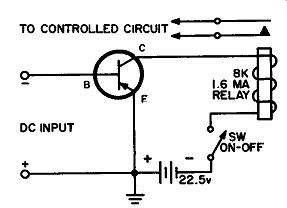
Fig. 802. Simple transistor amplifier can be used to operate a relay.
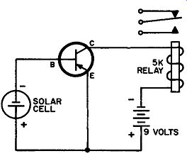
Fig. 803. Relay circuit will operate when solar cell receives light.
Relay amplifier
Just as the circuit in Fig. 801 permits us to use a less sensitive meter (and therefore a less expensive meter) so too can we use this circuit, or some variation of it, to give us an apparent increase in the sensitivity of other components. A relay is one such item.
Relays, like meters, are assessed in terms of their sensitivities.
Fig. 802 shows the relay circuit. The relay might require a current of one or more milliamperes to attract the armature of the relay toward its core. In the circuit of Fig. 802 a current of about 50 microamperes in the input will increase the collector current to the amount required to close the relay. Assuming this current to be 2 milliamperes (or 2,000 microamperes), the gain in our circuit is 40 (40 X 50 = 2,000). In this circuit the relay is the load.
In the circuits of Figs. 801 and 802, what would be our input? It could be some sort of signal which would give us the necessary amount of forward bias to activate the collector circuit. The input current could also be produced by a solar cell, as shown in Fig. 803.
Now take a few moments out to note the considerable similarity these circuits have.
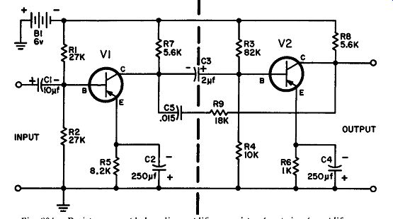
Fig. 804. Resistance-coupled audio amplifier consists of a pair of amplifiers,
one driving the other.
Preamplifier circuit
At first glance, the circuit in Fig. 804 looks far more complicated than any of those we have shown so far in this section. For this reason we have drawn a dashed line down the center of the circuit so that you can see for yourself that all we have here is just a pair of audio amplifiers, with the first amplifier driving the second.
We have analyzed the components in circuits similar to this one in earlier sections, but let's take out a few brief moments to do it again, just by way of review. If you will examine R1 and R2 you will see at once that these two resistors are in series. If you will trace their connections to battery B1 you will see that they are connected directly across it. These two resistors supply the correct amount of forward bias for V1. Now what about R3 and R4? Exactly the same as R1 and R2! They supply bias for V2.
Note that R1 and R2 do not have the same values as R3 and R4. If V1 and V2 are different you would expect their forward biasing requirements to be different also. The two transistors also use emitter bias. The emitter resistors, R5 and R6 are shunted by large values of capacitance--250 µf. These capacitors have a rating of 6 volts. While we're on the subject of capacitors, examine C1 and C3. These are also fairly large capacitance units (compared to the types used in vacuum-tube amplifiers) and are 25-volt electrolytics. We must watch our polarity in the case of electrolytics.

Fig. 805. Methods of connecting an electrolytic capacitor.
When considering the emitter bypass capacitors, remember that for p-n-p transistors the current flows from the emitter down to ground. This makes the top end of the emitter resistor minus and the bottom end plus. C2 and C4 are connected to observe this polarity.
In the case of C2 and C4 the matter of polarity is quite clear cut, but what do we do about coupling capacitors C1 and C3? It is entirely possible for a coupling unit to be connected to two positive voltage points, yet we must still be careful about polarity.
To see how we can come to a decision about this, please look at Fig. 805. In Fig. 805-A we have an electrolytic directly across a battery. There is no problem here since the plus terminal of the electrolytic goes directly to the plus terminal of the battery.
Similarly, the negative lead of the electrolytic is wired to the negative end of the battery. The electrolytic receives the full voltage of the battery and must be able to withstand it.
In Fig. 805-B, we are still observing polarity properly since the negative end of the electrolytic is connected to the arm of the potentiometer. But isn't point Ba positive point? Yes, it is, but it is less positive than point A. To simplify matters even further, we have eliminated the potentiometer in Fig. 805-C. Now you can see that we have connected the negative terminal of the capacitor to one of the positive terminals of the battery. This is point B. But so is point A. However, while point B is positive, it is less positive than point A. Another way of saying exactly the same thing is to say that point B is negative with respect to point A. Now getting back to Fig. 804, how do we know that we have connected C1 and C3 correctly, so that polarity is observed? In the case of C1 we don't know. We have not been told just what it is that C1 connects to. It is possible that in connecting C1 to its input we would find it necessary to turn C1 around.
We have no such doubts about C3. The collector of V1 to which this capacitor is connected is more negative than the base of V2, to which the capacitor is also connected.
R7 and RS are easy to identify. These are our collector load resistors. What is left? Just a series combination of C5 and R9.
This is our negative feedback circuit. It improves the stability of the amplifier and gives the amplifier a somewhat better frequency response.
We have gone through this amplifier rather hurriedly, since audio amplifiers were covered in an earlier section. A simple resistance-capacitance coupled amplifier of this sort could be used as an audio preamplifier.
Signal tracer
A signal tracer is just an audio amplifier plus a detector. The detector is generally a crystal diode as shown in Fig. 806. For the amplifier portion we could have used the circuit of Fig. 804, but we have added the one in Fig. 806 just to emphasize the fact that not all audio amplifiers are exactly alike. As an example, locate C3 (Fig. 806). If you will trace its connections you will see that it is shunted directly across the battery. The purpose of this capacitor is to maintain a low-impedance path around the battery.
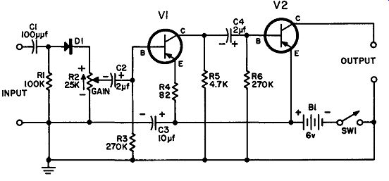
Fig. 806. The diode permits use of the audio amplifier as a signal tracer.
As long as the battery is fresh, or at least not too used, its impedance will be fairly low. But with time and use the internal resistance of the battery will rise, and long before a decision 1s made to discard it, will act as a common impedance or coupling device between stages. This can result in feedback between stages, producing amplifier instability. An electrolytic across the battery ensures a low-impedance path around it regardless of the condition of the battery. But before we decide that this is a wonderful cure all, remember that electrolytics also get old and that they have their own ills--including an increase in their own internal impedance.
Now examine the coupling capacitors in Figs. 804 and 806. How do they compare as far as capacitance and polarity are concerned? C3 in Fig. 804 has the same capacitance and the same positioning as coupling capacitors C2 and C4 in Fig. 806. But what about the input capacitors (C1 in Fig. 804 and C2 in Fig. 806)? Quite a difference here in several respects. Note the arrow in Fig. 806 showing the direction of current flow through the diode load resistor R2. When the slide arm is at the bottom end of the resistor the negative end of C2 is connected to the negative end of the battery. But suppose the slide arm is at the top end of the potentiometer. The lead of C2 is now at some plus point depending on the amount of current being rectified by the diode and the value of the gain control. This might be as much as 1 or 2 volts.
Now what about the other side of C2? This side of the capacitor is connected to the base of V1. From the base we have two ways of approaching the battery. One path is through a fairly high value of resistance (R3--270,000 ohms) to the negative terminal of the battery. The other path is through the transistor to the emitter, through 82-ohm emitter resistor R4 to the plus terminal of the battery. This latter path is so very much lower in resistance than R3 that the base (hence capacitor C2) is not too far removed (in terms of voltage) from the plus terminal of the battery.
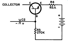
Fig. 807. Rearrangement of part of the circuit of Fig. 806 to show voltage
divider action.
Since this may not be too clear from an examination of the circuit, we have re-drawn it for you in Fig. 807. Consider the emitter and base of the transistor as a resistor of low-value in series with R4 and R3. These three components act as a voltage divider across the battery. But because of the very large value of R3, the plus connection of C2 is much closer, from a voltage view point, to the plus terminal of the battery.
While we are making comparisons between the two amplifiers, is there anything else we should notice? Yes--there are several items we should spot. V2 in Fig. 806 has no emitter resistor. The emitter resistor for V1 isn't bypassed. Also, the two transistors, V1 and V2 act as part of a voltage dividing network. In Fig. 804, however, we had an actual resistive voltage divider network (R1 and R2; R3 and R4) for forward bias. This arrangement is better than compelling the transistor to work in a resistive function.
Also, in Fig. 806 we have no feedback network. From all this you might conclude that Fig. 804 is the better circuit, and so it is. But before we toss out Fig. 806, consider the uses of the two circuits.
One is an audio preamplifier where we have some interest in stability and sound quality. The other is intended as a rather ordinary audio amplifier to be used as part of a test instrument.
It is possible that the difference between these two circuits may have been immediately apparent to you. Carry this sort of analysis along to transistor radio receivers and you will at least have learned a few of the reasons why there is a price differential among them.
Fig. 808. Sometimes radio components are drawn so that their function isn't too obvious. When this happens start tracing the circuit and all the parts will fall into their proper places.
Another audio amplifier
As long as we're examining audio amplifiers, let's take a look at the one shown in Fig. 808. This is a transformer-coupled unit, but a first glance seems to show some component arrangements worth investigating. The emitter circuit for V1 looks a bit odd until we examine it more closely and see that some of the components have been drawn in such a way as to make the circuit look peculiar. R4 and C3 we can recognize immediately as the emitter resistor and bypass capacitor. But what about R2, R3 and C5. We can't do much about these until we grope around a bit and locate RS. Look just a bit more carefully and you will see that R2, R3 and RS are all in series and that this series network is connected directly across the battery. What is this network? It supplies forward bias for V1. Similarly, R5, R6 and RS have the job of forward biasing V2.
What other information can we extract from this circuit? C4 in the output circuit of V1 might require a bit of thinking. The small value of C4 indicates that it is an rf bypass, somewhat unusual to find in an audio amplifier. However, if the input is supplied through a diode detector, we might find C4 necessary. It is possible, however, that the diode detector might have an rf bypass in its own output circuit, so C4 might be an unnecessary luxury. C7, in the output of V2 is a fixed tone-control capacitor.
Look Ma--no parts
The circuits we have examined so far in this section are certainly modest enough in their demands for parts, yet you could have a complete transistor receiver with still fewer components.
Fig. 809. Transistor radio receiver with a minimum number of parts.
We have the circuit in Fig. 809. And just in case you think that this is good for earphone reception only, we have included pro vision for a speaker.
A receiver of this sort will not have the sensitivity or selectivity of a six-transistor set, nor is there any claim of this sort being made. What we are interested in here is not in running a contest between receivers but in learning more about the functioning of transistor circuits.
With this caution in mind, what is there about Fig. 809 that can add to our storehouse of knowledge? You might think that the obvious absence of parts might clarify the situation.
The first item we might notice is that V1 is being used as a detector. The fact that it is marked detector is a sure-fire give away. How could we know, then, that it is a detector without the help of the label? There are several clues that demand attention.
V1 is located between a transistor (V2) being used as an audio amplifier and a tuning coil. Even if V2 were not marked, we see that it is connected to a phone jack. Consequently we can draw the conclusion that the input to V2 must be audio. And since the input is a tuned rf circuit (it would have to be with a 365 µ.µ.f tuning capacitor) then the only function left to V1 would be detection.
Suppose, though, we assume this isn't enough evidence. What more information do we have? What about the forward bias for V1? Actually, there is no forward bias other than that supplied by the input signal. And since this is the case, we may assume that the operating point on the characteristic curve must be in the vicinity of the cutoff point. In this circuit we depend on one-half of the input signal to supply enough forward bias to take the transistor out of cutoff. The other half of the signal will drive it further into the cutoff region. This is rectification, or, to give it its other name, detection.
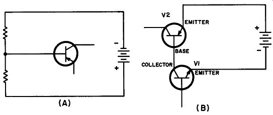
Fig. 810. A pair of transistors can be used as a voltage divider.
What about V2? Is it biased at all? Is it properly biased? Since we have a p-n-p transistor we want our emitter to be positive with respect to the base. We can see quite readily that the emitter connects to the plus terminal of the battery, but what about the base.
The return path to the minus terminal of the battery is through the emitter-collector circuit of V1. Before we decide this is not for us, consider the emitter-collector of V1 as a resistive path and you'll have no trouble getting back to the negative terminal of the battery.
Working with crystalline materials, as we are, does not necessarily imply that all our explanations are going to be crystal clear.
Earlier in this section we mentioned that a circuit diagram will often obscure an understanding of the theory. For this reason let us consider the biasing of V2 once again, but this time from the vantage point of Figs. 810-A and -B. In drawing A the biasing
arrangement for the transistor is the same circuit arrangement we have used so often in earlier sections. But what about drawing B? We don't have to connect the base of V2 into the divider since V2 and V1 in series act very much like the resistive pair shown in Fig. 810-A. Fig. 811. Grounded-collector amplifier. The true relationship of R'J to the transistor isn't clear until the circuit is redrawn.
Common-collector amplifier
We guarantee one thing. Once you get accustomed to the idea of circuit analysis, you will not be satisfied to look at a circuit without really seeing it as it is. Circuit analysis is guaranteed to keep your mental gear-box turning, and that is as it should be.
So, flexing our gray-matter muscles, we come across Fig. 811, which does not deceive us for a moment because of its simplicity.
We recognize it immediately as a grounded-collector amplifier, but classifying the circuit is just a small step. There aren't many components, so we can dispose of them fairly rapidly. C1 is a coupling capacitor connecting the circuit to a preceding stage or some signal source. Ditto for T1 except that it couples the output to the next stage.
Since R1 is the only component remaining, we might become sort of complacent and think that we have analyzed the circuit.
But have we? How is the circuit biased? And just what is R1 up to anyway? Since R1 is obviously involved in the biasing, answering one question will probably give us the solution to both.
Since this is a p-n-p transistor, we want a positive emitter and that is exactly what we do have. The emitter is connected to the positive terminal of the battery through the primary of T1. For this type of transistor we want the collector negative, and since both the collector and the minus terminal of the battery are grounded, that requirement is filled.
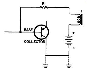
Fig. 812. The base and collector of the transistor of Fig. 8ll are considered
here as part of a voltage divider.
R1 is still dangling in mid-air and so is the question of how we get our forward biasing. The way the circuit of Fig. 811 is arranged isn't too much help in supplying an answer, so let us re-arrange the circuit as shown in Fig. 812. Once again we have a voltage
divider, but this time it consists of the primary of the output transformer in series with R1 and the base-collector circuit of the transistor. Think of the transformer primary winding as a resistor and the base-collector circuit of the transistor in the same light and you will see the voltage divider for what it really is. And here, just as in Fig. 810-A, the base is connected directly into the voltage divider for proper forward biasing.
What do we need for circuit analysis? Our first and most obvious need is to toss out complacency and for it substitute the realization that a circuit diagram is a convenience and as such it can often obscure as much as it explains. The second and not such obvious need is to re-draw that portion of the circuit diagram that is not absolutely clear so that its operation and function become evident.
This isn't an operation that will appeal to lazy people, so, if you wish, you can use it as a measure of character analysis.
Oscillators
Many people like to classify their ideas and their thoughts, and by putting them into compartments in their mind are able to keep all their facts nice and orderly. If we go along with this sort of thinking, a logical step would be to put all transistor circuits into two categories--amplifiers and oscillators. What we have talked about in this section are amplifiers, but it isn't such a big jump to oscillators as you might think. Some amplifiers will oscillate at the slightest opportunity and frequently we must take steps to make sure that they will not do so The very close relationship between a multivibrator type of oscillator and amplifier circuitry is very nicely illustrated by the drawing in Fig. 813. A quick look might convince you that what we have here is an ordinary resistance-coupled amplifier, but a single component, C2, changes all that. The output at the collector of V2 is in phase with the base-emitter circuit of V1. This is the sort of thing positive feedback is made of, a condition that leads to oscillation. Now you might insist that there is no input to V1, consequently there can be no signal feedback. It is true we have no external signal, something we would need if C2 were not present, but consider how unlikely it is that both V1 and V2 will conduct exactly the same amount of current at exactly identical moments. Any small voltage change at the collector of V1 will be sent along to the base input of V2, through C1. This small voltage change will be amplified by V2 and fed back to V1, through C2.
What could have caused the current in V1's collector circuit to change? This could have been the amplified effect of a very tiny change in the forward biasing of V1. It may seem odd to talk about a change in the forward biasing of V1 since what we have here is a de circuit. This change, though could consist of a very slight variation in the amount of current flowing between base and emitter. In what direction would this variation be--that is, would the change be such that the base emitter current increased? Or would it be a decreasing current? It makes no difference. We're not interested right at this point in knowing what the base-emitter current is up to. The important fact is that a change does take place. Please keep in mind, too, that the variation in base-emitter current is practically microscopic--if we can use such a word in connection with current.
That the change is tiny does not bother us either. For this minute change is amplified by V1, further amplified by V2 and is then fed back to V1 (via C2) in such a way that the extremely tiny change receives considerable support. Add the two--the small change and its highly amplified counterpart--and we now have the equivalent of an input signal.
The operation of a multivibrator is simple. Its explanation is quite complex. Briefly, what happens is that each transistor, V1 and V2, runs the gamut from cutoff to saturation. The output of this oscillator, when compared to the symmetrical sine waves produced by coil-type oscillators of the Hartley and Colpitts varieties, is highly distorted.
Crystal oscillators
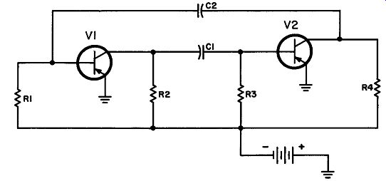
Fig.
813. The addition of a feedback capacitor, C2, changes the circuit from
a resistance-coupled amplifier to a multivibrator oscillator.
The silicon and germanium semiconductors we have covered in this guide form the very famous and highly-publicized duo of a rather large family of crystalline substances. Other crystals--such as quartz, and tourmaline--have their own, very legitimate claim to fame. These crystals act as true transducers and can change a mechanical strain to a voltage.
[1. A transducer is a substance or device which can change a force, such as torque, pressure, velocity, strain, shear, sound, heat or light, into a voltage, or conversely, can take a voltage and change it into sound, pressure, etc. A microphone is a transducer. So is a speaker. ]
The crystal is ordinarily placed between a pair of metal plates.
When the plates are connected to a voltage source, the crystal will distort. When the crystal is permitted to resume its natural shape once again, its action produces a voltage or electrical charge across the two metal plates which hem it in. But a crystal can no more resume its exact shape immediately, than a compressed spring can when released. What we will get will be a series of charges on the metal plates, each one smaller than the preceding. Again we can compare this to a spring whose expansions and contractions keep getting smaller and smaller. But we can keep the spring bouncing and we can keep the crystal in action by applying properly timed voltages. In this respect the crystal behaves very much like a coil in series with or in parallel with a capacitor. The coil-capacitor combination will resonate at a particular frequency, depending on its physical dimensions. So will the crystal.
With these facts safely tucked away, let's proceed to an examination of the crystal oscillator circuit of Fig. 814. We can recognize some old friends immediately, such as the emitter resistor R1 and its bypass capacitor Cl. We have also come across R4, the collector load, in other circuits. There are a few other components whose appearance or function may seem to be new. Start with the crystal.
It is represented by a pair of parallel lines used to indicate the metal plates sandwiching the crystal, shown as a rectangle. Shunted across the plates of the crystal is a radio-frequency choke coil, marked rfc. Neglecting the choke coil and the crystal for a moment, what about R2 and R3? These two resistors are in series but, as you can see, they are shunted directly across the battery. The base of the transistor is connected to the junction of these two resistors through the choke coil. The function of the two resistors now becomes evident. Since we have a p-n-p transistor, we want the base at a slightly lower positive voltage than the emitter and this is just what these two resistors do. Now we can also see the necessity for the radio-frequency choke coil. The de resistance of this coil is very low, possibly less than I ohm, and so the ba:se quite properly considers itself directly connected to the junction of R2 and R3.
The choke coil raises some technical questions in our thinking processes, and if it doesn't, it should. A little earlier we mentioned the action of the crystal in charging the metal plates which hold it.
But with a choke coil of just I ohm resistance, don't we have what amounts to a short across the plates? Yes, for de. But the varying charge on the crystal plates is ac and so for this type of voltage the choke coil could have an impedance of thousands of ohms.
How can we regard this circuit? Ignoring the base and the crystal for the moment, current will flow from the negative terminal of the battery, through R4, through the transistor from collector to emitter, through R1 to ground or the positive terminal of the battery. This is a direct current flow and we have done nothing to change it. But with our natural born penchant for disturbing the existing order you know by now that things are going to change.
Connected to the base we have a crystal which will act very much like a tuned circuit. But this tuned circuit, connected as it is between base and emitter, will vary the forward bias. This same crystal is not only in the base-emitter circuit, it is also located in the base-collector circuit. A small part of the energy of the output circuit is fed back to the input, overcoming its losses, and permitting continued oscillation.
More about the crystal
Fig. 814. Crystal-controlled transistor oscillator.
An oscillating crystal is a nice challenge to our mental processes because when we get right down to it, the crystal (and its holder) are mechanical. The challenge arises out of the fact that we had better think of it as electrical, if our crystal oscillator circuit is to make any sense. The crystal, though, doesn't hold any monopoly on mechanical devices which can be interpreted electrically or electronically. A stretched spring, released and then allowed to come back to a resting point after its wild back and forth gyrations have subsided, can be represented by a damped wave. The rotating armature of a generator results in a sine wave of constant amplitude.
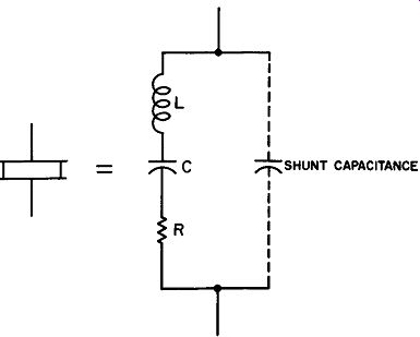
Fig. 815. A crystal and its equivalent electrical circuit. The shunt
capacitance and the series resistance are small and can often be disregarded.
Fig. 815 shows the equivalent circuit of the crystal. There is a certain amount of capacitance between the metal plates and, be cause this shunts the crystal, that is exactly the way in which we show it. The crystal itself behaves like a series-tuned circuit and since every tuned circuit has a certain amount of resistance associated with it, it isn't too surprising to find R in series with L and C. Unfortunately, in a generalized circuit of this form, values of R are not given, and since one unmarked resistor looks very much like another, we have no way of knowing whether R is large or small. In the case of the crystal, more so than in the case of actual tuned coil and capacitor arrangements, R is very low.
R, though, influences Q directly, and so the crystal, because of the very low amount of R, has a very high Q. With this information on hand, circuit analysis of Fig. 814 resolves itself very nicely as we see in Fig. 816. R, in series with L and C (in Fig. 815), has been omitted since there is less need for its inclusion than in an actual coil-capacitor circuit. Since C and L form a series circuit, it will have its minimum impedance at its resonant frequency. At any other frequency than the resonant one, the impedance of L and C rises quite dramatically.
The net effect of this electronic behavior is to give us an oscillator that works at a single frequency, so much so that crystal oscillators are often used as frequency control circuits or where single frequency stability is the prime consideration.
Now what about the choke coil, RFC, in Fig. 816? We still need it, for the substitution of the electrical equivalent of the crystal just serves to emphasize that without the choke we would have no de return from the base of the transistor to ground-that is, to the plus terminal of the battery.
If you can't lick 'em--join 'em.
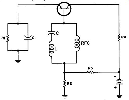
Fig. 816. The crystal-oscillator circuit becomes somewhat more understandable
when the electrical equivalent of the crystal is substituted for it.
The most positive cure for a headache is decapitation. This is quite a drastic cure for what may be a very minor illness. Similarly, the shunting capacitance existing between the metal plates of a crystal is usually nothing more than just a slight annoyance, particularly since the overall shunting effect of the circuit itself may be so much greater.
Somewhat unexpectedly, we sometimes shunt capacitance directly across the crystal plates. Offhand, it would seem as though additional capacitance would be extremely undesirable, yet it can be made to work in a very beneficial way. We can use it to tune the crystal within small limits. Or, we can use this capacitance as an ac voltage divider. Or both. Fig. 817 shows how.
A circuit analysis of this illustration shows how few new parts demand our attention. R3 and C1 are old-timers we've discussed in connection with other circuits. R1 and R2 are immediately recognizable as a voltage divider for forward biasing. R4 is the collector load. Other than the battery and the transistor, all that we have left in the way of components to study is the crystal and a pair of capacitors, C2 and C3. C2 and C3 are in series, and this series combination is shunted directly across the plates of the crystal holder.
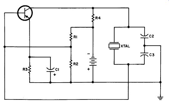
Fig. 817. This crystal oscillator circuit uses a capacitive voltage
divider. Feedback is through CJ to the base-emitter circuit.
Now join us in a bit of mental transposition. In place o( the crystal, visualize the electrical equivalent as shown earlier in Fig. 815. We can disregard the shunt capacitance since it will simply add to the equivalent capacitance of the series combination of C2 and C3. Similarly, we can forget about resistor R of Fig. 815.
What is left? Just a series-connected inductor and capacitor in place of the crystal.
With the crystal in oscillation, an ac voltage at the resonant frequency will appear across the plates of the crystal holder. C2 and C3 are shunted across this voltage and will promptly divide it between them. Equally? Only if C2 and C3 are equal. If they are not of equal capacitance, the unit with the smaller capacitance will get the larger amount of voltage. Thus, we can control the division of voltage through proper selection of the relative capacitances of C2 and C3.
If you will trace the circuit you will see that the base is connected directly to the bottom end of C3 while the top end of C3 goes to the emitter. Offhand, this might seem incorrect, since, if you will move along from the top of C3 (on your way to the emitter), you will promptly run into C1. But the capacitance of C1 is so much greater than C3, that we can disregard it completely. Thus, if C1 is 1 uf and C3 is 100 uuf, the ratio is 10,000 to 1.
The voltage produced across C3 is fed back to the input since it is quite clearly connected in the base-emitter circuit. But the crystal and C2 and C3 are part of the collector circuit. In this way, a selected amount of output voltage, depending on the ratio of C3 to C2, is fed back to the input. And if we also arrange for proper phasing, we have met all the conditions necessary for sustained oscillation.
Oscillators and amplifiers
It is very nice to be able to put things into mental compartments.
Designating a transistor circuit as an oscillator or as an amplifier falls into this category, but while it is convenient, it is also mis leading. It tends to give us the impression that a wide chasm exists between oscillators and amplifiers. But is the separation as wide as we might think? If we have an amplifier we can feed back part of the output, in phase, to the input. Would we then have an oscillator? Not necessarily. We would have a regenerative amplifier but it would not oscillate until the feedback reached a certain amount. Thus, the transition from amplifier to oscillator is not as clear and as sharply defined as we might have expected.
And now that we have managed to bring about an apparently closer relationship between oscillator and amplifier, let's separate them again. What is the difference? With an amplifier we select a particular operating point on the characteristic curve and that point determines our class of operation. An oscillator of the L-C type, though, runs the gamut from cutoff to saturation and back again. For an understanding of just what it is that a transistor does, then, we must always go to its characteristic curve.
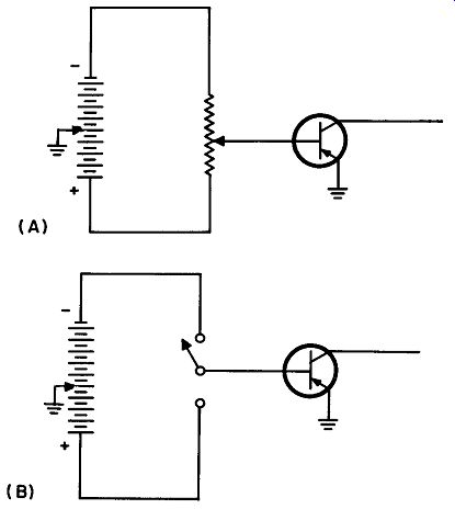
Fig. 818-A, -B. In this arrangement, the transistor input is forward-
or reverse-biased, depending on the position of the potentiometer arm
or the switch.
Transistor as a switch
We can use selected portions of the transistor characteristic curve or all of it for amplifiers and oscillators, but if we wish we can also use the beginning of the characteristic (cutoff) and the end (saturation). Cutoff means no current while saturation is maximum current. This all-or-nothing-at-all state of affairs is what we get every time we use a switch.
Fig. 818-A shows our first step toward using the transistor in this function. When the arm of the potentiometer is at the top, the transistor is heavily forward-biased and we get maximum, or saturation, current. When the arm is at the opposite end, the base emitter circuit is heavily reverse-biased and we are at cutoff. To get a faster transition from cutoff to saturation, we could substitute a single-pole double-throw switch for the potentiometer.
We want to use the transistor as a switch since it will be faster and much more dependable than manual switching. That is why the circuit of Fig. 818-B, using a switch to control the bias, is self-defeating. But instead of a switch, we can control the biasing electronically, as shown in Fig. 819.
Let's analyze the circuit and see what we have. Since we have a p-n-p transistor we must have the emitter positive, the base and the collector negative with respect to the emitter. Tracing the circuit shows that it meets these requirements, within limits. With the help of potentiometer R2 we can vary the amount of bias to the base-emitter circuit. When the arm is at the top, we get the maximum amount of forward biasing. Let us say that the voltage of the battery is sufficient to produce maximum transistor current--that is, saturation. This condition is comparable to having a closed switch.
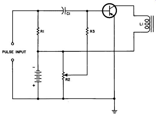
Fig. 819. Transistor switching circuit. The transistor has two operating
points-saturation and cutoff.
Finale!
And so we come to the end of our story-but not yours. What you have had in this guide is to transistors what an appetizer is to a heavy ten-course dinner. Just the beginning. But if you have managed to follow the text then you are well-equipped to move on to a more detailed study of transistors.
If you will examine R1 and R2, you will see that they are in series, but these two series-connected components are shunted across the pulse input. If we inject a strong positive-going pulse, the resulting current flow through R1 and R2 will produce a voltage that will be in opposition to the battery voltage. If this voltage is strong enough, it will reverse-bias the input and drive the transistor down into cutoff. Through proper selection of pulse amplitude and frequency we can work our transistor just as you would an ordinary light switch you have in your home-but much faster. Transistor switches are used in computers and in equipment that is pulse-operated, such as radar units and television receivers.
QUIZ
1. Describe the operation of a meter amplifier. What would be the advantage of using such a circuit?
2. Draw the circuit of a simple transistor-operated relay amplifier and explain how it works.
3. Describe several methods of connecting an electrolytic capacitor in a circuit. What problems are involved in making the connections?
4. What is a signal tracer?
5. If a circuit diagram is drawn so that you cannot immediately understand the functioning of some of the components, what can you do to overcome this difficulty?
6. Explain how transistors can be used as voltage dividers.
7. Draw a common-collector amplifier circuit and explain how it works.
8. Draw a multivibrator circuit and explain its operation.
9. What is a transducer? Give three examples.
10. Draw the circuit diagram of a crystal-controlled transistor oscillator.
11. What is the purpose of the shunting capacitor across a battery?
12. What are typical values of coupling capacitance used in transistor audio amplifiers?
13. Are the transformers used in transistor audio amplifiers step up or stepdown types. Explain the reason for your answer.
14. What is meant by circuit analysis? What is the advantage of being able to do a circuit analysis?