AMAZON multi-meters discounts AMAZON oscilloscope discounts
A transistor is a three-electrode device, the connections being to base (designated B or b), emitter (designated E or e), and collector (designated C or c). Invariably (except when a transistor is being used as a diode), one electrode is common to both input and output circuits-usually the emitter (common emitter), or sometimes the base (common base). The common-collector configuration is little used.
DC PARAMETERS
The four main parameters governing the dc performance of a transistor are:
input voltage
input current
output voltage
output current
Capital letters are used to designate average voltages and currents, and lowercase letters to designate instantaneous volumes of voltage or current:
V for average voltages, v for instantaneous voltages I for average currents, i for instantaneous currents
For example: VB, Vc, Ve means average values of base, collector, and emitter currents respectively, and vb, v,, ve means instantaneous values of base, collector, and emitter current, respectively. IB, IC, 1e means average values of base, collector, and emitter currents, respectively, and ib, means instantaneous values of base, collector, and emitter currents respectively.
Where instantaneous total values of voltage or current are referred to, a capital subscript is used, with a lowercase letter designating voltage or current. Thus vB, vc, vE mean instantaneous total values of base, collector and emitter voltage respectively, or iB, ic, iE mean instantaneous total values of base, collector and emitter current respectively.
It is also necessary to define the electrodes between which these voltages or currents apply. This is done by using the appropriate letters in the subscript:
VBE Vbe v3V E V ,CE ce V vCE BC V bc VBC
= average base-emitter voltage
= instantaneous base-emitter voltage
= instantaneous total base emitter voltage
= average collector-emitter voltage
= instantaneous collecto-emitter voltage
= instantaneous total collector-emitter voltage
= average base-collector voltage
= instantaneous base-collector voltage
= instantaneous total base -collector voltage
Logically, these should conform to the voltage direction (positive to negative), depending on whether the transistor is a PNP or NPN type, as in the following order:
PNP transistor = EB, BC, BE (or eb, bc, be)
NPN transistor = BE, CB, EB (or be, cb, eb)
INPUT CHARACTERISTICS
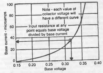
The input characteristics of a transistor show the variation of input current with input voltage. In the common-emitter configuration, input is to the base, and base current (Ib) is plotted against the base voltage measured between the base and emitter (Vbe ). In the common -base configuration, input is to the emitter, so the input characteristics show the variation of emitter current (Ie) against emitter voltage measured between emitter and base (Vb).
These relationships are given graphically in Fig. 15-1. The input resistance in each case is the reciprocal of the slope of the curve and is therefore low. Because the input characteristics are non-linear (shown by a curve rather than a straight line), input resistance is not constant but depends on the current at which it is measured. Because of the non-linear characteristics of the input, a transistor is normally current biased and driven from a current rather than a voltage source. This is provided by using an effective source resistance which is large in comparison with the input resistance. If this resistance (or, correctly speaking, impedance) is not high enough to swamp the varying resistance (impedance) of the transistor under drive, there will be considerable distortion of the input signal.

Fig. 15-1. Typical transistor input characteristics. --- Note - each value
of collector voltage will have a different curve.
Input resistance at any point equals base voltage divided by base current
TRANSFER CHARACTERISTICS
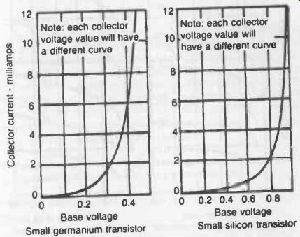
Transfer characteristics of a transistor are normally given as a plot of collector current against base current,

Fig. 15-2. Typical transistor transfer characteristics.
Fig. 15-2. Ideally, this should be a straight line. Any departure from a linear (straight line) relationship implies non-linear distortion of the output signal.
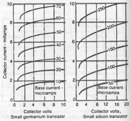
Collector volts Small germanium transistor
Collector volts, Small silicon transistor

Fig. 15-3. Typical transistor output characteristics.
OUTPUT CHARACTERISTICS
Output characteristic curves of a transistor show what is effectively switch-on voltage (or knee voltage as it is called), above which a large change in collector voltage produces only a small change in collector current. Since resistance is again the reciprocal of the slope of this I/V curve, it follows that output resistance of a transistor is characteristically high. The value of the collector current, and to some extent the slope of the curve, also depends on the base current. Separate curves are thus plotted for (constant) base currents, see Fig. 15-3. Again, note that a constant base current is only obtained with a high source resistance in the base circuit. Also, any non-linearity in the transfer characteristics of the transistor shows up on the input characteristics as uneven spacing of the curves for equal increments in input current.
CURRENT AMPLIFICATION
A transistor is generally used as a current amplifier. Here, the base current controls the current in the emitter -collector circuit, although it may only be a small percentage of the emitter current. Current can be added in the usual way. Thus, emitter current equals collector current plus base current; or, alternatively, base current equals emitter current minus collector current.
In expressing the characteristics of the transistor, collector current divided by emitter current is designated a, and collector current divided by base current is designated al, Knowing either a or a', it is possible to find the currents at the other electrodes since a = al/(1 + a') and al = a/(1 - a) Actual values of a and al can vary with frequency and current for the same transistor. Straightforward, simple, analysis of transistor characteristics is based on low signal currents at zero frequency, i.e., small changes in direct current. To make this clear, the symbols ao and aol are sometimes used, the subscript "o" indicating zero frequency.
The current amplification factor in common-emitter configuration (input to the base) is given by al (or aol). It is largely independent of collector voltage, but is usually measured at some constant collector voltage. Specifically, the value of al is directly related to the slope of the I /I curve, or the transfer characteristics.
It is also called the small-signal gain of the transistor. Actual values may range from as low as 10 up to several hundreds.
In the common-base configuration, with input to emitter, the current amplification factor is designated a (or a.) and is equivalent to the slope of the I/I curve. In this case, I is always a little less than I , so the value of a is always less than unity; typically of the order of 0.98.
DC CURRENT GAIN
Specifically, this is the ratio of Ic/Ib, in common-emitter configuration and is generally referred to as Beta (strictly speaking Beta ') or li, the latter normally being the parameter quoted by manufacturers. Beta and-hFE are not identical, and both vary with collector current. The quoted hFE value is therefore normally associated with a specific collector current. Commonly available transistors may have values of hFE varying from about 10 to 560 at collector currents ranging from 1 mA to 30 A. Here are some examples:
Low and medium power germanium transistors; typical hFE range 30 - 200 at collector currents from 1 mA to 300 mA.
Small signal high frequency germanium transistors; typical hFE range 30-100 at collector currents from 1 mA to 10 mA.
Germanium power transistors; typical hFE range 40-150 at collector currents from 500 mA to 1A.
Small signal silicon transistors; typical fFE range 50-500 at collector currents from 0.1 mA to 50 mA.
Medium power low frequency silicon transistors; typical hFE r 90-200 at collector currents from 10 mA to 150 mA.
High power low frequency silicon transistors; typical hFE ran 25-100 at collector currents from 150 mA to 5 A.
Small signal high frequency silicon transistors; typical hFE ran 40-100 and collector currents from 1 mA to 25 mA.
MANUFACTURER'S SPECIFICATIONS
Manufacturers' normally provide curves showing the static (dc), characteristics of industrial transistors for both common emitter and common base configurations, together with other characteristic values as appropriate. Summarized transistor data in catalogs or data sheets shout give at least the following:
VCEO (max) = maximum collector to emitter voltage on open current.
VCBO (max) = maximum collector to base voltage on open current.
VEBO (max) = maximum emitter to base voltage on open current.
Ic (max) = maximum collector current.
Pt (max) or Ptot (max) = maximum total power dissipation.
dc current gain (usually quoted as a typical figure at a specific collector current).
To assist selection, such listings may be arranged in groups of (roughly) similar types, on the lines given previously. It is even more helpful when the design application is also shown for each transistor type, such as general purpose, switching, audio amp, etc. The following is a useful classification and guide:
Germanium Transistors
small, medium -current, switching and general purpose.
medium -current switching, low power output.
small, medium -current amplifiers.
af amplifiers, low power output.
complementary pairs.
high power output (power transistor).
Silicon Transistors
af amplifiers, small signal, general purpose.
af amplifiers, low level, low noise.
small -signal amplifiers.
rf amplifiers and oscillators.
medium-current switching, low power output.
high frequency, medium powers.
general-purpose switching.
power transistors.
Any reference to "power" grouping is largely arbitrary since there is no universal agreement on the range of power levels (referring to the maximum power rating of the particular transistor). Thus, low power may generally be taken to cover 100-250 mW, but such a grouping may include transistors with power ratings up to 1 watt. Similarly, medium power implies a possible power range of 250 mW to 1 W (but may extend up to 5 watts). Any transistor with a power rating of greater than 5 watts is classified as a power transistor.
Information about selecting transistors for characteristics is given in the next section.