The transistor first appeared as a working device in 1947, since which time it has been manufactured in hundreds of millions. It took a little time to realize that the same techniques used for producing individual transistors could be applied to complete circuits and sub-circuits containing both active components (e.g., diodes and transistors) and passive components (e.g., resistors and capacitors), with all necessary interconnections in a single unit familiarly known as a "chip." Apart from the obvious advantage of being able to produce complete circuits and sub-circuits in this way, the cost of producing a complex circuit by photo-etching techniques is little more than that of producing individual transistors, and the bulk of the circuit can be reduced substantially since transistors in integrated circuits do not need encapsulation or canning, and resistors and capacitors do not need "bodies." Another advantage is the potentially greater reliability offered by integrated circuits, since all components are fabricated simultaneously and there are no soldered joints. (Performance can also be improved as more complex circuits can be used where advantageous at little or no extra cost.
The next big step in integrated circuit construction was the development of microelectronic technology or extreme miniaturization of such components and integrated circuits. Photo-etching is readily suited to this, the main problem being in checking individual components for faults due to imperfections in the manufacturing process, and achieving a high yield of fault-free chips per "wafer" manufactured. Rejection rates are liable to rise with increasing complexity of the circuit, but modern processes now achieve a very high yield.
Basically, an integrated circuit consists of a single chip of silicon, typically about 1.25 mm square (0.050 inches square) in size.
Each chip may contain 50 or more separate components, all inter connected (although they may contain very many less for simpler circuits). The actual manufacturing process is concerned with producing wafers, each of which may contain several hundred chips.
These wafers are processed in batches, so one single batch production may be capable of producing several thousand integrated circuit chips simultaneously, involving a total of tens of thousands of components.
It is this high production yield which is responsible for the relatively low price of integrated circuits--usually substantially less than the cost of the equivalent individual components in a chip produced separately, and in the case of some chips even less than that of a single transistor. The final selling price, however, is largely governed by demand. The integrated circuit is a mass-production item and the greater the demand for a particular chip, the lower the price at which it can be sold economically.
Figure 1 shows a typical--and fairly simple--IC produced as a flat "package" encapsulated in plastic. The drawing is approximately 1 1/2 times actual size (9.4 mm long by 6 mm wide). Figure 2 shows the complete circuit contained in this IC, comprising 16 transistors, 8 diodes and 13 resistors. Figure 1-3 shows the physical appearance of the chip, much magnified, when it is part of the wafer. The actual size of this chip is approximately 2.5 mm by 2 mm.
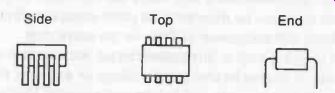
Fig. 1. Outline shape of a typical 8-pin dual-in-line integrated circuit,
about 1 1/2 times actual size.
The actual component density or number of components per unit area, may vary considerably in integrated circuits. The figure of 50 components per chip has already been mentioned, which is typical of small-scale integration (SSI). It is possible to achieve much higher component densities.
With medium-scale integration (MSI), component density is greater than 100 components per chip; and with large-scale integration (LSI), component density may be as high as 1000 or more components per chip.
Both MSI and LSI are extensions of the original integrated circuit techniques using similar manufacturing methods. The only difference is in the matter of size and physical separation of the individual components and the method of inter-connection.
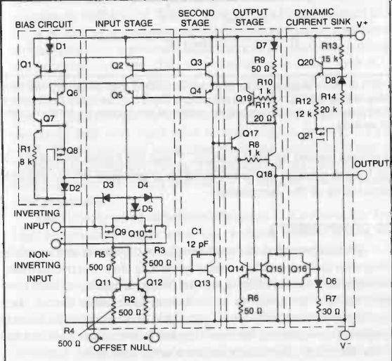
Fig. 2. Schematic diagram of one half of a CA3240 BiMOS operational amplifier
showing components and interconnections all formed in the substrate of the
chip.
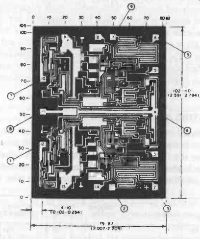
Fig. 3. Much enlarged illustration of the CA3240 chip containing two complete
circuits like Fig. 2. Actual dimensions of this chip are 2.5 by 2 millimeters.
Grid dimensions marked around the outside of the diagram are in thousandths of an inch.
MONOLITHIC AND HYBRID ICs
Integrated circuits where all the components and connections are formed in the substrate of the "chip" are known as monolithic ICs. There is a further class of ICs where the individual components (transistors, diodes, resistors, etc.), or even complete sub-circuits, are all attached to the same substrate but with interconnections formed by wire bonding. These are known as hybrid ICs.
In hybrid circuits, electrical isolation is provided by the physical separation of the components.
IC COMPONENTS
Transistors and diodes are formed directly on the surface of the chip with their size and geometry governing their electrical characteristics as well as density level, etc. Where a number of such components are involved in a complete integrated circuit their performance is usually better than that of a circuit with discrete (separate) components because they are located close together and their electrical characteristics are closely matched.
Resistors can be formed by silicon resistance stripes etched in the slice, or by using the bulk resistivity of one of the diffused areas.
There are limits, however, to both the range and tolerance of resistance values which can be produced by these methods. "Stripe" resistors are limited to a minimum width of about 0.025 mm (0.001 in.) to achieve a tolerance of 10 percent. Practical values obtained from diffused resistors range from about 10 ohm to 30 K-o, depending on the method of diffusion with tolerances of plus or minus 10 percent. Better performance can be achieved with thin-film resistors with resistance values ranging from 20 ohm to 50 K-o. A method of getting round this problem when a high resistance is required is to use a transistor biased almost to cut-off, instead of a resistor, in an integrated circuit where a resistance value of more than 50 K-ohm is required. This is quite economic in the case of integrated circuit manufacture and is a method widely used in practice.
Capacitors present more of a problem. Small values of capacitance can be produced by suitable geometric spacing between circuit elements and utilizing the stray capacitance generated between these elements. Where rather higher capacitance values are required, individual capacitors may be formed by a reversed-bias PN junction; or as thin-film "plate" type using a tiny aluminum plate and a MOS (metal-oxide-semiconductor) second plate. The former method produces a polarized capacitor and the thin film method a non-polarized capacitor. The main limitation in either case is the relatively low limit to size and capacitance values which can be achieved-typically 0.2 pF per 0.025 mm (0.001 in.) square for a junction capacitor and up to twice this figure with a thin film MOS capacitor, both with fairly wide tolerances (plus or minus 20 percent). Where anything more than moderate capacitor values are needed in an integrated circuit it is usually the practice to omit the capacitor from the circuit and connect a suitable discrete component externally.
Both resistors and capacitors fabricated in ICs also suffer from high temperature coefficients (i.e., working values varying with temperature) and may also be sensitive to voltage variations in the circuit.
Unlike printed circuits, it is not possible to fabricate inductors or transformers in integrated circuits at the present state-of-the art. As far as possible, therefore, ICs are designed without the need for such components; or where this is not possible, a separate conventional component is connected externally to the integrated circuit.
From the above it will be appreciated that integrated circuits are quite commonly used as "building blocks" in a complete circuit, connected to other conventional components. A simple example is shown in Fig. 4 using a ZN414 as a basic "building block" in the construction of a miniature AM radio. Although it is a high gain device (typical power gain 72 dB), the integrated circuit needs a following stage of transistor amplification to power a crystal ear piece; high value decoupling capacitors; and a standard coil and tuning capacitor for the tuned circuit. The complete circuit is capable of providing an output of 500 millivolts across the earpiece, with a supply voltage of 1.3 and typical current drain of 0.3 milliamps.
THE SHAPE OF ICs
ICs come in various "package" shapes. Quite a number have the same shape (and size) as a typical transistor and are only readily identified as an IC because of the greater number of leads emerging from the bottom (a transistor usually has only three leads).
These shapes are defined by the standard coding adopted for transistor outlines, e.g., TO-5, TO-18, etc., which also identifies the individual pins by numbers (e.g., see Fig. 5D, E and F).
Other ICs come in the form of flat packages with leads emerging from each side. These are three different arrangements used (see Fig. 5A, B, C, and G).
Dual in-line, where the leads on each side are bent down to form two separate rows to plug directly into a printed circuit panel or IC holder (A and B).
Quad in-line, like dual in-line, except that the leads on each side form two parallel rows (G).
Flat, where the leads emerge straight and from each side of the package (C).
In all cases leading numbering normally runs around the pack age, starting from top left and ending at top right (again see Fig. 5). The number of leads may be anything from eight to sixteen or even more.
Some types of holders designed to match standard pin configurations or flat shape ICs are shown in Fig. 6. These holders have pin configurations similar to the ICs they take. Their principal ad vantage is that they can be soldered to a printed circuit or Veroboard, etc., with no risk of heat damage to the IC itself since this is only plugged in after soldered connections are completed.
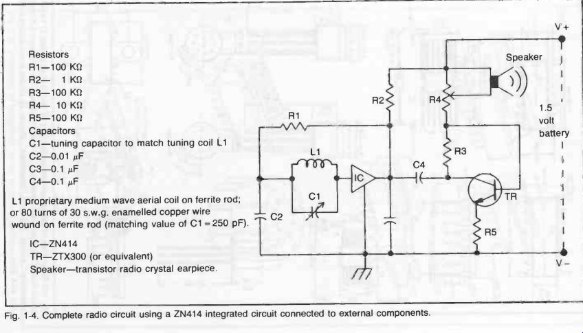
Fig. 4
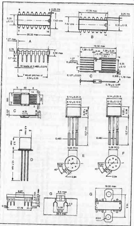
Fig. 5. Examples of integrated circuit designs. A 16-pin dual in-line. B
14-pin dual in-line. C flat (ceramic) package. D 3-lead transistor "can" shape.
E 6-lead "transistor" shape. F 8-lead "transistor" shape.
G 12-pin quad in-line with heat sink tabs.
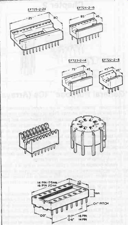
Fig. 6. Examples of integrated circuit holders (Electro-value).
Most circuit constructors, however, prefer to solder ICs directly to a printed circuit panel (or Veroboard).