The description "general purpose" is not accepted terminology but it is used here to describe integrated circuit chips which comprise a number of individual components, usually transistors and possibly also diodes, each component in the chip connecting to individual outlet leads. Thus by connecting to the appropriate leads an individual transistor (or diode) can be connected to an external circuit. Other chips of this type may also include components connected within the chip, e.g., transistors in Darlington pairs, but the same principle of application applies. The technical description of such a chip is an integrated circuit array.
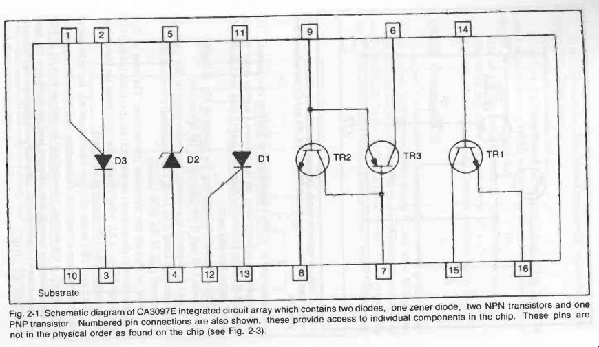
Fig. 1
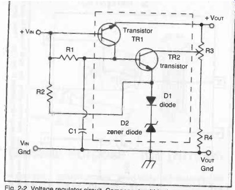
Fig. 2.
Voltage regulator circuit. Components within the dashed outline are in the
CA3097E integrated circuit. R1, R2, R3, R4 and C1 are external components.
A simple example of such a chip is shown in Fig. 1. It consists of three transistors (two interconnected); two types of diodes; and a zener diode. This particular chip is used in the voltage regulator circuit described in Section 8 (Fig. 8-4), using two of the transistors, the SCR diode and the zener diode.
This circuit design is shown in Fig. 2. The components to be utilized which are contained in the IC are enclosed in the dashed outline, i.e., TR1, TR2, D2 and D3. The other components in the chip (D1 and TR3) are not required. Resistors R1, R2, R3 and R4 and a capacitor C, are all discrete components connected externally.
Figure 2-3 re-examines the component disposition of the chip, together with the necessary external connections. Note that the arrangement of the leads or pin-out arrangement does not necessarily follow the schematic diagram (Fig. 1) where the pins are in random order to clarify connections to internal components. The actual pin-out arrangement on ICs follows a logical order reading around the chip. Schematic diagrams may or may not follow in the same order (usually not).
Connections for completing the circuit of Fig. 3 are:
Leads 1, 2 and 3 are ignored as D1 is not used.
Lead 4 connects one side of the zener diode to the common earth line and Lead 5 to Lead 13, connecting the zener diode to the correct side of the SCR (diode).
Now to pick up the transistor connections. The base of TR1 (15) connects to the external resistor R1; and the collector lead (14) to the other side of R1, which is also the input point for the circuit.
The emitter lead (16) connects to output.
TR2 and TR3 in the chip are interconnected, but only one of these transistors is required. Connecting lead (6) to (9) shorts out TR2, which is not wanted.
Connecting the emitter lead (8) of TR3 to 11-12 (already joined); the collector lead (9) to (6); and the base lead (7) to the center tag of the external potentiometer R3 connects TR3 into the circuit.
It only remains tor the external components to be completed. These are:
R2 to lead (14) and lead (12).
Capacitor C to lead (6) and earth point. Lead (10) on the IC is also the substrate or earthing point of the IC, so should also be connected to the common earth line.
One end of the potentiometer R3 to the top (output) line.
The other end of the potentiometer R3 to R4.
The other end of R4 to the bottom common earth line.
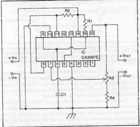
Fig. 3. Completed voltage regulator circuit showing wiring connections made
to the integrated circuit. Pins in this diagram are shown in the actual physical
order they appear on the integrated circuit. Note. For clarity the integrated
circuit is drawn much larger in proportion to the external components.
SPARE COMPONENTS
A number of components in an array may not be used in a particular circuit, but the cost of the single IC can often be less than that of the equivalent transistors or diodes ordered separately and used individually to complete the same circuit. The circuit using the IC will also be more compact and generally easier to construct.
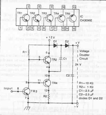
Fig. 4. Schematic diagram of CA array (top) and voltage doubler circuit
using TR2, TR3 and TR4 from the array together with external components.
The spare transistors in the array (TR1 and TR5) can be used instead of separate diodes, connected for diode working by ignoring the collector leads.
A little study sometimes shows where further savings are possible. Figure 2-4, for example, shows a voltage doubler circuit for a 1 kHz square wave input signal, based on a CA3096E IC array which contains 5 transistors.
Only three of these transistors are used in this particular circuit, leaving two "spare." The circuit calls for two diodes D1 and D2 (as well as three resistors and two capacitors) to be added as discrete components.
Transistors can also be worked as diodes (by neglecting the collector lead), and so the functions of D1 and D2 could be performed by the two "spare" transistors in the array (thus using up all its components).
Alternatively, since the current needs a square wave input signal, the two "spare" transistors could be used in a multivibrator circuit to provide this input. Since diodes are cheaper than transistors, this is a more economic way of using all the components in the original array.
The fact that popular ICs are quite cheap means that it is seldom worth while going to elaborate methods of trying to use all the components available in an array, unless such utilization is fairly obvious, as above. Using only part of an array can still show savings over the purchase of individual components for many circuits.
The astable multivibrator circuit shown in Fig. 5, for example, only uses one of the three complete switching circuits contained in the CA3600E array, associated with an OTA CA3080 integrated circuit and four external resistors. On the other hand, Fig. 6 shows a high gain amplifier circuit using all the components in the CA3600E array with external resistors.
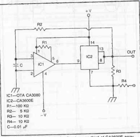
Fig. 5. Astable multivibrator circuit using one third of CA3600E array.
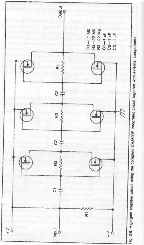
Fig. 6
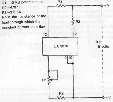
Fig. 7. Constant current circuit using components found in CA3018 array.
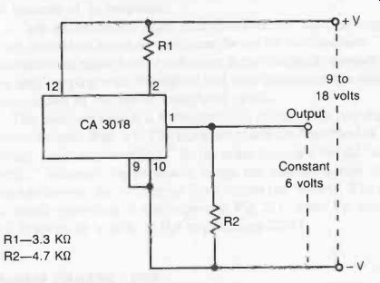
Fig. 8. Circuit giving a constant 6 volts output from a 9 to 18 volts supply
voltage, again using the CA3018 array.
CONSTANT CURRENT CIRCUIT
A useful circuit employing the CA3018 integrated circuit array is shown in Fig. 7. This array comprises four transistors (two …and four diodes). Tapping the super-alpha pair of transistors, a constant current source can be produced, the magnitude of this current being set by adjustment of the potentiometer R1 over a range of about 0.2 mA to 14 mA, depending on the actual supply voltage.
The same integrated circuit can also be used as a constant voltage source--Fig. 8. In this case the constant voltage output is the zener voltage of the transistor worked as a zener diode, which is approximately 6 volts.