Many circuits have been presented throughout this guide, and there are probably several you would like to build and/or experiment with.
Two or more circuits may be combined to create your own custom projects. This final section will give you a few tips on constructing electronic projects.
BREADBOARDING
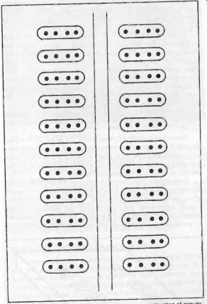
Fig. 1. A solderless socket is used for temporary construction of circuits.
If you are experimenting with a circuit, you want to be able to make solderless connections that can easily be altered. You may have to try several combinations of component values before get ting the exact results you want. Soldering, unsoldering and re-soldering can be tedious at best. Mistakes can be disastrous.
Repeated solderings increase the chances of cold solder joints and unreliable connections. Even more importantly, some components (especially semiconductors like integrated circuits) can be ruined by excessive heat.
Fortunately, there is a much more practical way to set up temporary circuits-the breadboard. In its simplest form, this is merely a solderless socket that the various component leads and wires can quickly be plugged into or pulled out of. The various holes in this type of socket are electrically interconnected. The most commonly used interconnection pattern is illustrated in Fig. 1.
While solderless sockets of this type are inexpensive and readily available, there may be times when you will prefer to create your own customized solderless socket with Fahrnstock clips, as shown in Fig. 2. Interconnections are made between the clips with ordinary hook-up wire. This type of home-brew breadboard may be necessary when large or unusually shaped components, which won't fit in a standard solderless socket, are used.
A solderless socket can make experimentation and circuit de sign much easier, but it is even more useful as part of a complete breadboarding system. A typical system of this type is shown in Fig. 3.
These breadboarding systems consist of a solderless socket and various commonly used sub-circuits, such as power supplies and oscillators. These sub-circuits can be separate, stand-alone modules used along with a simple solderless socket, but it is generally more convenient to have them grouped together within a single, compact unit, as shown in the photo. In either case, these sub-circuits will be needed far too often to make breadboarding them from scratch each time they're needed reasonable. Frequently employed sub-circuits should be permanently constructed.
Most breadboarding systems also have one or more potentiometers and switches available for convenient use in experimental circuits.
Remember to make all changes with the power off to reduce the risk of damaging some components (especially ICs and other semiconductors) or, in some cases, suffering severe injury your self. Bear in mind at all times that electrical shocks can be very painful, or even fatal-always use caution.
Some circuits might not work well (or at all) in a standard solderless breadboard. This is usually true in high frequency circuits where the length of connecting wires, "phantom" components (especially inductances and capacitances) and shielding (or lack thereof) can become critical. Fortunately, the circuit which can not be prototyped in a breadboard socket is very much the exception to the rule. If high frequencies are involved in the circuit you are working with, keep interconnecting wires as short as possible. If the circuit operates incorrectly or erratically, try relocating some of the components.
Somewhat more common are circuits which may change their operating parameters noticeably when a more permanent type of connection is used. Be aware of this potential problem.
There really isn't much you can do about it in advance, but at least you can be prepared to recognize such problems when they do crop up.
At least, you'll be able to save a lot of time and hair pulling.
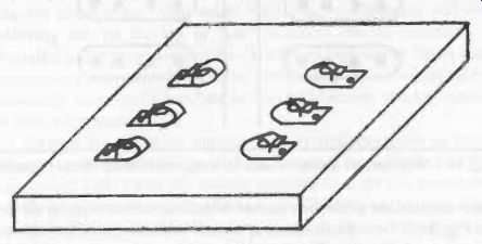
Fig. 2. You can create your own customized solderless socket with Fahrnstock
clips.
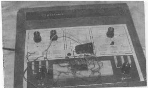
Fig. 3. A breadboarding system consists of a solderless socket and standard,
commonly used sub-circuits.
PERMANENT CONSTRUCTION METHODS
Once you have designed your circuit, breadboarded the project, and gotten all of the bugs out, you will probably want to re build some circuits in a more permanent way. Solderless bread boarding sockets are great for testing and experimenting with prototype circuits, but they really aren't much good when it comes to putting the circuit to practical use.
Breadboarded circuits, by definition, have nonpermanent connections. In actual use, some component leads may bend and touch each other, creating potentially harmful shorts. Components may even fall out of the socket altogether when the device is moved about. Interference signals can easily be generated and picked up by the exposed wiring.
Generally, packaging a circuit built on a solderless socket will be tricky at best. They tend not to fit very well in standard circuit housings and boxes. Besides, a solderless socket is fairly expensive. It is certainly worth the price if it is re-used for many different circuits. But if you tie it up with a single permanent circuit, you're only cheating yourself. Less expensive methods that are more reliable, more compact, and that offer better overall performance are readily available.
Some relatively simple circuits can be constructed on a perforated circuit board, with component leads and jumper wires soldered directly together, using point to point wiring. Only very, very small, very simple circuits should ever be wired directly together without any supporting circuit board. Otherwise you will end up with a "rat's nest" of jumbled wiring that is next to impossible to trace if an error is made, or if the circuit needs to be serviced or modified at a later date. In addition, a lot of loose hanging wires can create their own problems, such as stray capacitances and inductances between them, allowing signals to get into the wrong portions of the circuit.
"Rat's nest" wiring is also just begging for internal breaks within the wires, and short circuits between them. Momentary, intermittent shorts may not cause permanent damage in all cases, but they can result in some strange circuit performance that can be maddeningly frustrating to diagnose and service.
Symptoms of "rat's nest" wiring can also be a problem with some complex circuits on perf boards. Always try to minimize crossings of jumper wires. Use straight line paths for jumper wires when ever possible. The circuit should be laid out for the minimum possible number of jumpers. Some will probably be unavoidable, but limit them whenever possible.
You should also try to position all of the components on the board to see how they'll fit before you even plug in your soldering iron. This will help you avoid unpleasant surprises, like ending up with no place to put that big filter capacitor.
For moderate to complex circuits, or for circuits from which a number of duplicates will be built, a printed circuit board gives very good results. Copper traces on one side (or, in very complex circuits, on both sides) of the board act as connecting wires between the components. Very steady, stable, and sturdy connections can be made, since the component leads are soldered directly to the supporting board itself.
Great care must be taken in laying out a PC board to eliminate wire crossings. Traces cannot cross each other. If a crossing is absolutely essential, a wire jumper must be used.
Stray capacitances between traces can adversely affect circuit performance. In critical circuits, a guard band between traces can help reduce the potential problem.
Especially in circuits using ICs, the copper traces are usually placed very close to each other. This means a short circuit is very easy to create. A small speck of solder, or a piece of a component's excess lead could easily bridge across two adjacent traces, creating a short. Only small amounts of solder should be used. Too much will flow and bridge across adjacent traces.
Tiny, near invisible hairline cracks in the copper traces can also be problematic, if you're not careful. Generally, fairly wide traces that are widely spaced are the easiest to work with. However, this isn't always practical with all circuits-especially where ICs are used.
A printed circuit board type of construction results in very short component leads. Lengthy leads aren't needed. This can help minimize interference and stray capacitance problems.
More and more circuits being constructed today use the wire-wrapping method. A thin wire is wrapped tightly around a square post. The edges of the post bite into the wire, making a good electrical and physical connection without soldering. Components are fitted into special sockets that connect their leads to the square wrapping posts. This form of construction is most appropriate for circuits made up primarily of a number of integrated circuits. If just a few discrete components are used, they can be fitted into special sockets, or soldered directly, while the connections to the ICs are wire-wrapped (hybrid construction). In circuits involving many discrete components, the wire-wrapping method tends to be rather impractical.
Wire-wrapped connections can be made (or unmade) quickly and easily, without risking potential heat damage to delicate semi conductor components.
There are some disadvantages to this type of construction. Discrete components are awkward at best. The thin wire-wrapping wire is very fragile, and easily broken. It can only carry very low power signals.
The wiring can be very difficult to trace.
Still, when many ICs are involved (some circuits require several dozen), wire-wrapping is a very convenient form of construction.
SOCKETS
People working in electronics disagree strongly about the use of IC sockets. Some technicians say sockets should only be used for chips that are frequently changed (such as ROMs containing different programming), or possibly for very expensive ICs. Others (myself included) recommend the regular use of sockets on all ICs.
It may seem silly to protect a 25¢ IC with a 50C socket, but what you are really protecting is your own time and sanity. If you make a mistake, or if an IC has to be replaced for servicing, you will have to desolder and resolder each individual pin, watching out for solder bridges and over-heating. Frankly, I don't think it's worth the trouble. Sockets don't add that much to the cost of a project, and they can head off a lot of grief and frustration if problems do arise. Think of them as sort of an insurance policy.
There are some cases in which sockets are undesirable. In equipment for field use which is likely to be bounced around a lot, direct soldering may be desirable, to prevent a chip's pins from being bounced out of place.
A few (very few) high frequency circuits can be disturbed by the slightly poorer electrical connection of a socket. But these are few and far between. In 99% of the circuits you'll work with, using IC sockets will cause no problems and could save you from a lot of needless hassle.
Length of square area- inches
Length of square area- millimeters
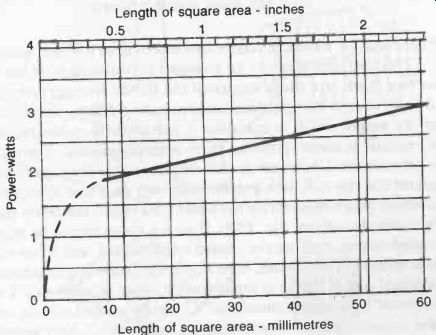
Fig. 4.
This graph can be used to determine the size of squares of copper required
for heat sinks on printed circuit boards. Size is given as length of a
square. Any other shape of the same area can be used (see text).
HEAT SINKS
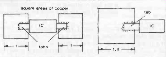
Fig. 5. Copper area determined from Fig. 4 is for two equal squares
(one at each end of the IC). If a single square is used at one end of the IC,
its area needs to be slightly greater for the same heat dissipation.
Where integrated circuits handle moderate powers and a heat sink is necessary to dissipate heat generated within the IC itself, areas etched on the copper of a printed circuit board can conveniently be used as heat sinks. ICs which are suitable for heat sinks of this type are usually fitted with a tab or tabs for soldering directly to the copper bands forming the heat sink.
The area of copper needed for a heat sink can be calculated quite simply, knowing the relevant circuit parameters. First it is necessary to determine the maximum power to be dissipated, using the formula:
Power (watts) = 0.4 V^2 / 8R_L + Vs x Id L
… where:
Vs is the maximum supply voltage
Id is the quiescent drain current in amps under the […]
RL is the load resistance (e.g., the loudspeaker resistance in the case of an audio amplifier circuit).
Strictly speaking the value of Vs used should be the battery voltage plus an additional 10 percent, e.g., if the circuit is powered by a 12-volt battery, the value of Vs to use in the formula is 12 + 1.2 = 13.2 volts. This allows for possible fluctuations in power level, such as when using a new battery.
If the circuit has a stabilized power supply, then Vs can be taken as this supply voltage.
The quiescent drain current (Id) is found from the IC parameters as specified by the manufacturers and will be dependent on supply voltage. Figures may be quoted for "typical" and "maximum." In this case, use the maximum values.
Figure 4 then gives the relationship between power to be dissipated and copper area, based on a maximum ambient temperature of 55 °C (which is a safe limit for most IC devices).
Example:
Supply voltage for a particular Ic is 12 volts. Load resistance if 4 ohm and the maximum quiescent current drain quoted for the IC at this operating voltage is 20 milliamps. The supply volt-age is not stabilized, so the value to use for Vs is 12 + 1.2 = 13.2 volts 13.22
Thus power = 0.4 x 8 x 4 + (13.2 x 0.020) = 2.178 + 0.264 = 2.422 watts (say 2.5 watts)
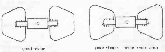
Fig. 6. Good and poor shapes for heat sink areas on PCBs.
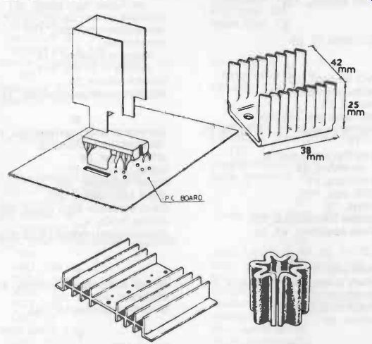
Fig. 7. Examples of external heat sinks for fitting to power transistors
and integrated circuits.
From Fig. 4, a suitable copper area is seen to be a 40 mm square.
This heat sink area can be arranged in two squares (if the IC has two tags); or a single square (if the IC has one tag) (see Fig. 5). Of course, the area does not have to be a square. This is simply the easiest shape to calculate. It can be rectangular, regular or irregular in shape, provided there is sufficient area. A point to be borne in mind, however, is that with any shape the copper area nearest the tag will have greater efficiency as a heat dissipator, so shapes which concentrate the area in this region are better than those that do not (see Fig. 6). If such a shape cannot be incorporated conveniently on the printed circuit layout, and a less efficient shape has to be used, then it may be necessary to increase the actual area of copper to compensate. Copper areas given in Fig. 1 should be adequate since most ICs can be worked at fairly ambient temperatures without trouble (e.g., up to 70 °C). Very approximately this higher temperature operation will be provided by a copper area of a little more than one half that given by the graph, so there is a fair margin for error available when using this graph.
The graph also shows that the area of copper necessary to dissipate powers of 3 watts or more tends to become excessive, compared with the area of printed circuit panel actually required for the circuit itself. Where higher powers have to be dissipated, there fore, it is usually more convenient (and more efficient) to dissipate heat by an external heat sink fitted to the IC itself. Some examples of external heat sinks are shown in Fig. 7.