AMAZON multi-meters discounts AMAZON oscilloscope discounts
OSCILLATORS
Synchronous systems need a clock. There are many oscillators that can serve as the basis for a system clock. We mention a few here. Some of the criteria influencing the selection of an oscillator are cost, stability, and frequency range.
The Schmitt Trigger Oscillator
This is about the least expensive and simplest oscillator you can make. FIG. 10 shows the circuit, which uses an R-C combination to cause the oscillation.
This circuit will continue to oscillate reliably as long as power is applied. The Schmitt trigger oscillator suffers from a lack of stability-the clock frequency is not precisely constant. Another mild disadvantage is the 30 percent duty cycle of the square-wave output. If you want a perfectly symmetric square wave, you may run the output into the clock input of a JK flip-flop wired in toggle mode.
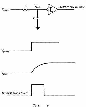
FIG. 9. A power-on reset circuit.
This produces a flip-flop output transition at every rising edge of the oscillator.
The flip-flop thus provides a clock with one-half the frequency of the oscillator.
In the Schmitt trigger oscillator, the capacitor continually charges and discharges between the hysteresis points. When the capacitor charges to the upper trip point, the output will switch to low. This will discharge the capacitor until the lower trip point is reached, which causes the output voltage to go high. The cycle repeats indefinitely.
The 555 Oscillator
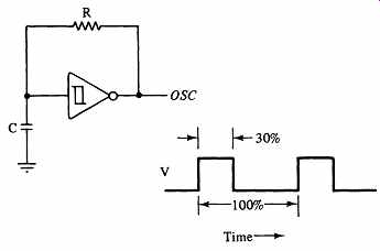
FIG. 10. A simple Schmitt trigger oscillator. Rand C control the frequency.The 555 Timer is a low-cost integrated circuit built for timing industrial
devices.
It can be configured as a single shot or as an oscillator. One of the virtues of the 555 Timer is the slow oscillation frequency that can be achieved with capacitors of moderate size. It is also more stable than the Schmitt trigger oscillator. This is a popular chip-a fine choice for clocks with periods slower than several microseconds. FIG. 11 shows the 555 Timer wired as an oscillator. The values of Rand C determine the frequency of oscillation; consult the data sheet for timing computations.
Crystal-Controlled Oscillators
A variety of integrated circuit clock chips derive their frequency from an external quartz crystal. The Motorola MC12060 and MC12061 are examples of chips that permit a wide range of clock frequencies that are determined by the oscillation frequency of the quartz crystal. The MC14411 is useful for clocking data trans mission, since the chip provides a large selection of standard clock frequencies, including such popular ones as 110, 300, 1200, and 9600 Hz. The chip uses a crystal of fixed frequency (1.8432 MHz) and has internal logic to reduce this frequency to the values selected by the control inputs. Another excellent wide range oscillator is the RCA CD4047.
The disadvantage of these chips in general synchronous design is their fixed frequencies, which preclude any gradual varying of the clock rate in debugging.
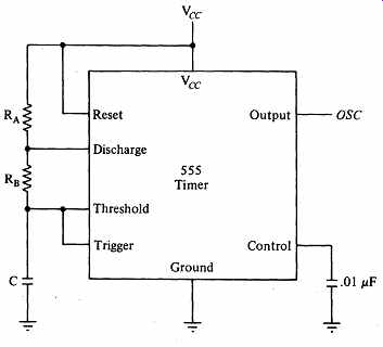
FIG. 11. The 555 timer used as an oscillator. RA , Rs, and C control
the frequency.
The System Clock
Remember that in synchronous system design, we usually want more from a clock than just an oscillating logic signal. In Section 6 we designed a useful system clock that supports an automatic clock derived from an oscillator, and also a manual mode that permits the designer to issue manual clock transitions.
The oscillator forms the first stage of such a system clock.
Also, remember that system clocks for synchronous circuits must often drive many chips, so the clock's output must be well buffered to provide the necessary operating power.
SWITCH DEBOUNCING
Mechanical switches are important parts of digital devices, but they present signals that are unsuitable for use in digital logic circuits. The switch contacts do not open or close cleanly; they undergo a period of "bounce" in which the electrical signal from the switch will change noisily between its voltage extremes many times in the course of a few milliseconds. A switch debouncer removes the bounce by responding to only one of the voltage excursions during each switch operation. In Section 4 we analyzed this situation and offered a solution that used RS flip-flops.
Here we repeat these circuits, and discuss the component values and the electrical efficiency of the solutions. FIG. 12 shows two switch-debouncing circuits, each using a single-pole, double-throw toggle switch and gates from the 74 LS logic line.
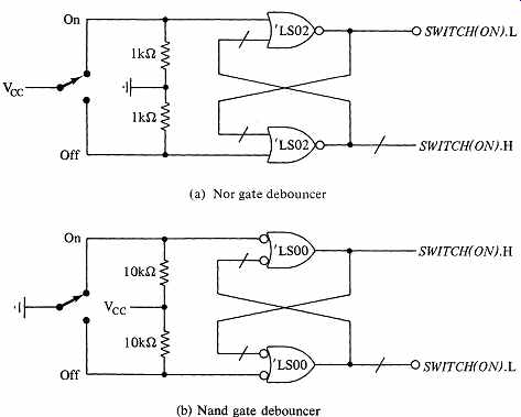
FIG. 12
Consider the circuit in FIG. 12a. Whenever the switch closes the On contact, the voltage on that line goes to ground (L) and causes the cross-coupled gate flip-flop to record truth on the SWITCH. ON outputs. Once the flip-flop responds to the On signal, further bounces on the line will have no effect on the outputs. The debouncer will register a change only when the Off contact closes, at which time the debouncer will respond to only one of the Off bounces.
The resistors have a pull-up or pull-down function to assure a proper default H or L voltage level at the gate inputs. We derive the values of the resistors in FIG. 12a by noting that when a contact is open the current path is from the gate input through a resistor to ground. The 74LS02 input requires a maximum of 0.4 mA current in the L state. We must make sure that the voltage at the gate input does not rise above the low-level logic threshold of 0.8 V; for safety, we will choose 0.4 V as our maximum allowable low-level voltage. Then:
0.4 - 0 Rmax = 0.0004 = 1000 G
The maximum suitable resistance value is 1 k-Ohm. To calculate the resistance in FIG. 12b, we must ensure that the voltage at a gate input is at a valid H level when the switch is open. Choosing 3 V as our lower limit for H, and using lIB = 20 uA for 74LS gates, we have
5 - 3 Rmax = 0.00002 = 100 k-Ohm
In our circuit, we showed a smaller resistance value, 10 k-Ohm. There is a small advantage in the circuit in FIG. 12b, since it consumes less power. Except during switching transitions, one side of the switch is always closed, so there is a virtually constant 5 V drop across one of the resistors. The current drawn by this circuit is 5 mA for FIG. 12a, which is equivalent to 12 or more normal 74LS loads. In FIG. 12b, the circuit draws only one-tenth of this current, and so is about equivalent to one 74LS load. The power saved in FIG. 12b can be significant if the design has several debounced switches.
This illustrates the typical reasoning when choosing values for pull-up or pull-down resistors in digital circuits. In most cases, only Ohm's Law is needed, coupled with the ability to identify the important issues.
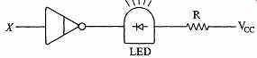
LAMP DRIVERS
It is often necessary to display critical signals in a digital system. Gates seldom have enough current-handling capability to drive lamps as well as other gates, so it is usually necessary to isolate the lamp from the logic signal by an open collector buffer. We may use standard buffers that will load the logic signal with one additional standard TTL current load; alternatively, Darlington buffers are available that require close to zero input current.
In digital display, the incandescent lamp has given way to a solid-state device called a LED (light-emitting diode). LEDs have the advantages of low cost, low power drain, and long service life. The brightness of a LED is a function of the current passing through it. Most LEDs are limited to currents of about 10 mA. Higher currents produce more light but shorten the life of the
LED. The typical LED driver circuit is:
where the open collector gate might be a 7406 buffer or a 9667 Darlington buffer.
If the input signal X is H, the output of the open collector inverter is L, and the LED will light. The resistor R limits the current through the LED. We may determine a suitable value for R using Ohm's Law. The voltage at the output of the open-collector gate is close to zero; the voltage drop across the LED itself is about 1.6 V when it is conducting, regardless of the current. Thus for a 5 V power supply, the voltage drop across resistor R when the LED is lit is (5 - 1.6 - 0) = 3.4 V. If we wish to limit the current through the LED to
5 mA, then R = § = ~ = 6800 I 0.005
A resistor in the range of 700 to 1000 0hm would be appropriate.
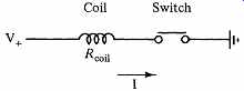
DRIVING INDUCTIVE LOADS
Mechanical relays, solenoids, and motors depend for their operation on coils of wire, which exhibit electrical inductance. Although inductance is sometimes useful, it can cause difficulties for the digital designer who wishes to switch an inductive load on and off. Even at low voltages, inductance can damage switches.
Inductance tends to stabilize current by resisting changes in current through the coil. Consider a coil containing a sufficient length of wire to provide a safe current-limiting resistance when the coil is connected between its design voltage and ground:
-- With the switch closed, the current is given by Ohm's Law:
1= Vcc
Rcoil
When the switch is opened, the resistance across it rapidly moves from zero toward infinity. Ohm's Law predicts that the current would rapidly drop to zero, but the inductance in the coil prevents the current from dropping immediately.
Where can this current go? The inductance creates a large transient voltage across the switch, polarized to maintain the flow of the current across the switch.
In many cases, the voltage becomes great enough to create a spark across the switch's contacts. If the switch is a switching transistor, the voltage surge will destroy it unless it is protected. Even mechanical switches will burn out unless they are robust or otherwise protected.
Protecting Switches with Diodes
In dc circuits, a diode across the coil will protect the switch from damage: When the switch is closed, the diode is back-biased and no current flows through the diode. When the switch opens and the inductance tries to maintain the current, the voltage rises at the switch terminal, and the diode becomes forward biased. Current can flow in a circular path through the diode until the inductive effect has dissipated. Therefore, no large voltage surge is developed across the switch.
Protected by diodes, switching transistors can safely switch many inductive loads. The IN4000 series of diodes is useful for bypassing common inductances arising with relays and solenoids.
Solid-State Relays
For switching heavy dc or ac loads, we recommend a solid-state relay. These devices are carefully engineered to amplify weak logic signals to the level where they can drive a final switching transistor for dc loads or a TRIAC for ac loads.
The logic switching component is often optically isolated from the relay, providing excellent protection to the digital circuit driving the relay. When using a solid state relay to switch a dc load, you should still protect the relay from dc voltage surges by using an external diode, as described previously.
THE OPTICAL COUPLER
When interfacing distant or dissimilar devices, we frequently wish to assure that electrical problems at one end of the system will not damage components at the other end. As long as there is an electrical connection between elements of a system, we face the risk of one malfunctioning element damaging another. For instance, the Teletype produces its signals from electromechanical circuits. A mechanical short circuit within the Teletype might produce violent electrical disturbances on the serial signal lines.
Fortunately, there is a non-digital device called the optical coupler or optical isolator that uses light instead of electrons to pass signals. The optical coupler has a light-emitting diode as its input component and a phototransistor as the output, sealed together in one unit. You are already familiar with the light emitting diode. In a phototransistor, the switching action is controlled by light shining on the base of the transistor rather than by electrical current flowing through the base. When current flows through the light-emitting diode, it lights up. The phototransistor, which is off (switch open) when the diode is dark, responds to the light by closing its transistor switch. FIG. 13 shows the optical coupler circuit in its customary notation.
There is no electrical connection between the input and the output sections; within wide ranges of power supply voltages, the input and output stages are electrically independent of each other. It is this property that proves so valuable in protecting or isolating systems.
The principal disadvantage of the optical coupler is its relatively slow switching speed; 1 to 100 u-sec is typical performance-much slower than digital logic circuits, but satisfactory in many data communication applications.
POWER SUPPLIES
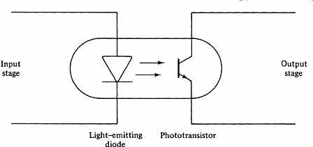
FIG. 13. An optical coupler.
Power supplies are nondigital devices, and the construction of a good power supply is something of a mystery. Although the elements of power-supply technology are easy to understand and primitive supplies appear simple to construct, it usually pays to purchase them unless you have a good understanding of analog design techniques. Usually, you get what you pay for, and usually you are paying for things other than volts and amperes-for example overload protection, service life, voltage regulation, efficient cooling methods, compactness, and ability to run at high ambient temperatures.
A typical power supply has four major components, shown in FIG. 14.
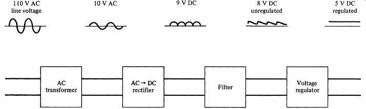

FIG. 14. Components and waveforms of a dc power supply.
The raw power comes from the power company as 110 or 220 Vac. A transformer lowers the voltage to several volts above that required by the supply output. A full-wave rectifier changes this alternating voltage to a bumpy dc version. A filter smooths this waveform, producing a somewhat fluctuating voltage slightly above the desired one. Finally, a voltage regulator removes the last fluctuations and fixes the output voltage at the precise level desired.
Remote Sensing
Quality power supplies have a remote sensing feature to compensate for the small voltage drop generated in the conducting paths connecting the power supply with the circuit. Two small wires (sense wires) sample the voltage in the circuit itself and feed this voltage back to the power supply so that it can regulate the voltage into the digital circuit rather than the voltage produced at the power supply. The sense wires can be small, since they carry virtually no current.
Integrated-Circuit Voltage Regulators
Commercial power supplies often provide all the components in FIG. 14 (and other refinements) in one package, providing regulated power that must then travel to the digital systems. Another approach is to use regulators contained in an integrated circuit chip. These can supply a few amperes at fixed voltages and can be an economical way to supply power. They have the advantage that all the analog complexities of power regulation are wrapped up inside the package; troubleshooting is reduced to swapping components.
The main power supply, without the regulation section, is easier to build than the complete supply. This approach allows us to furnish unregulated power to each circuit card and to perform the voltage regulation right on the card, a design that tends to minimize ground loops and other undesirable power distribution phenomena discussed in the next section. However, on-board regulation places a major heat-producing element on each logic card, making efficient heat dissipation essential.
POWER DISTRIBUTION
In digital logic, well-developed formalisms exist for solving problems in terms of the pure binary concepts of truth and falsity. What happens when these binary concepts are emulated by voltages? If the voltages are clean and stable, digital hardware provides a reliable correspondence between the logic values and the voltage levels. If the voltages are noisy or unstable, we are no longer in the true digital domain and unpleasant things can happen.
Two common problems that remove us from a simple binary world are the generation and distribution of power. Chips require power, and a circuit with many chips may require much power. You should develop an intuitive under standing of where current is flowing in digital circuits and what effect that flow has upon noise generation. Fortunately, it is not difficult to gain this understanding.
Every integrated circuit package has a pair of power pins. In the TTL logic family, these pins are Vcc and ground. We do not (and should not) show these pins on logic diagrams, since they are not logical in nature. Vcc is a source of current that flows into the chip and out through the ground pin. The chip accepts voltages representing logical signals as inputs and uses a portion of the supply power to produce voltages for logical output signals. The conversion of power is never 100 percent efficient. The lost power appears as heat, and the chip warms up. The circuit assembly must be able to dissipate this heat, or the chip's temperatures may rise to the point that the circuits behave improperly.
Losses in Power Distribution Systems
Resistive losses. FIG. 15 shows two gates powered by the same power supply; the inevitable resistances of the power distribution system are lumped in the diagram for convenience. The Rv terms are resistances associated with Vcc distribution; RG is ground distribution. For the sake of our exposition, let us assume that each gate requires 10 mA of operating current and that all resistances are zero except RG1 , which is 10 Ohm. The voltage at the ground pin of gate 1 will be 100 mV above the power supply (system) ground. This comes from Ohm's Law:
E = I x R = 0.01 x 10 = 0.10 V
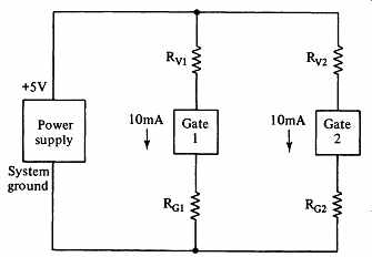
FIG. 15. Two gates powered by one supply, with resistance in the power-distribution
system. Line resistances are lumped for convenience.
Logic inputs and outputs are omitted.
Each gate produces logical output signals referenced to the internal ground voltage of the integrated circuit chip. Suppose that each gate produces an output of I volts in the low voltage level and h volts in the high level. Gate 1 produces outputs of I + 0.1 V and h + 0.1 V with respect to the system ground. Now suppose that the output of gate 1 goes into the input of gate 2. Since RG2 is zero, gate 2 is operating with its internal ground equal to the system ground.
The 0.1 V offset of gate 1' s output reduces the noise margin at gate 2, since the gates have a maximum threshold with respect to their own internal grounds, above which they will not interpret a signal as a low voltage level. The offset at gate 1 is in the direction that moves gate 2's input closer to the threshold, thereby reducing gate 2's margin for error. In 74LS TTL, the low-level noise margin is 0.3 V. In our example, instead of a 0.5 V low-level signal, gate 2 would receive 0.6 V; only 0.2 V remains of the safety factor to handle other types of voltage disturbance.
Inductive losses. Ten ohms is an intolerably high resistance in a power circuit, and almost any power-distribution system will have resistances much lower than this. Don't relax! The problem may still be with you. We used resistances in the example above because they provided us with a simple, static example. The real villain is inductance. Inductance exists in any conductor, independent of resistance, and it depends on the geometry of the conductor. An inductor will generate a voltage across itself if the current it carries changes.
For a given inductance, the faster the rate of change of the current, the larger is the voltage across the conductor.
Now look again at FIG. 15. The power distribution resistances are typically a few milliohms, and we can usually neglect them. As long as each gate draws constant current, the rate of change of current is zero. The induced voltage due to the inductance of the power paths will also be zero, so we have no problem. Unfortunately, the power-supply current drawn by a gate surges up and down when its logic output changes. This phenomenon is particularly acute in TTL, the most popular logic family. Since any useful logic system will have changing internal logic signals, we have no alternative but to reduce stray inductances to a minimum. Circuit geometry is the only avenue available to us.
We will discuss several fabrication techniques for combating inductance.
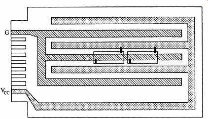
FIG. 16. A circuit board with strip power busses. Two integrated circuit
chips are attached.
Combating Inductance in Power-Distribution Systems
Ground planes. Solid-sheet conductors have the lowest possible inductance, and it is almost independent of the sheet's thickness. The best system is to mount integrated circuits on such a plane and connect the chip's ground pins to it. Piercing the plane with small holes to allow the other pins to pass through the ground plane to the other side of the board has virtually no harmful effect.
Strip distribution. Many commercial integrated-circuit packaging systems have interdigitated (interleaved) strip busses for power distribution, as shown in FIG. 16. In the section on TTL integrated-circuit data sheets we showed that noise margins in the L state are often smaller than in the H state, so we want the lowest possible inductance on the ground distribution system. Inductance is proportional to length, so in FIG. 16 we should use the bus marked G for ground since it has the shortest run to the supply pin on the edge connector.
Wire distribution. A round wire has much more inductance per unit length than a strip bus; it is usually pointless to try to use wire for power distribution on a printed circuit board. Nonetheless, wires are usually necessary to carry power from the power supply to a digital system. There are two ways to reduce the wire inductance-stranding and changing the shape to a flat braid.
Flat braid is stranded wire that has been rolled into strip form, thereby gaining the low inductance of strips while retaining the flexibility of woven wire.
Many commercial systems use laminated bus bars to distribute ground and V cc in a system. These bus bars have low inductance and low resistance, and also represent a distributed capacitance useful for filtering high-frequency noise.
For power distribution on printed circuit boards, bus bars often allow the use of two-sided rather than multilayered boards.
Recommendations. If you are new to digital logic systems, we strongly recommend that you use a commercial ground-plane system for your first few projects. This will keep you safely in the digital domain and make success more likely.
Some commercial ground-plane systems are expensive, but you can justify them if the system will see extensive use. Be prepared to pay more for power supplies, power distribution, and circuit cabinetry than you pay for the integrated circuits.
For small systems, printed circuit cards with a power bus on one side and a ground plane on the other are available at low cost. They are more desirable than a one-sided interdigitated bus card.
Bypassing the Power Supply
Even a distribution system with the least inductance will need help in order to deliver clean, stable power to the integrated circuits. The solution is a capacitor.
NOISE
The function of the capacitor is to store charge that can power the surges of an integrated circuit when its outputs change. The ideal geometry is to place a capacitor directly across the Vcc and ground pins of each chip. In a sense, this capacitor is a local power supply that is inexpensive enough to dedicate to each chip and will thereby have short leads and low inductance. More properly, it is a power averager that supplies surge demands and is then recharged from the main power supply. A capacitor used in this way is called a bypass capacitor, since the surges of current are absorbed in the capacitor and bypass the power supply.
Most capacitors come with round wire leads that have a high inductance per unit length. A rule of thumb is to keep these leads less than 3 mm long.
Only certain types of capacitors have low enough internal inductance to be useful for bypassing. Ceramic capacitors have low internal inductance and are suitable if in the range 0.01 to 0.1 uF. Ceramic dielectric disks are commonly used because of their small cost.
Tantalum dielectric capacitors also have low internal inductance and more capacitance per unit volume than ceramics, but with higher price. It is good practice to bypass the power supply leads with a 10 /LF tantalum capacitor where the leads enter the circuit card, in order to handle any current surge remaining from the smaller bypass capacitors at the individual chips.
A common mistake is to mount one bypass capacitor per chip on interdigitated power strip cards, but across the wrong strips. The correct way is the shortest possible path through the capacitor between the Vcc and ground pins of a chip.
The wrong way will force the surge current from a chip to go all the way to the end of a strip and back down an adjacent strip to reach the bypass capacitor.
Short is beautiful in digital fabrication!
So you have done a fine job on the algorithmic and architectural phases of your digital design, your logic implementations are flawless, and you have constructed your circuit neatly on a circuit board with a good ground plane and well-bypassed power supply. Is everything just fine? Not necessarily. Despite all your efforts, noise may still be a problem. Noise is unwanted voltage on the signal lines.
Good digital logic design attacks noise at the logical level. For instance, in synchronous design we process information only at certain fixed times governed by a clock signal, so that we are sure that, in our design, all the vital signals are stable. After a clock edge, we expect a certain amount of turbulence on the signal lines as they adjust to their new status, but this will die out long before the next edge. Similarly, we avoid using asynchronous inputs as decision variables, since we cannot control when they change.
However, other sources of noise arise from the physical layout of the hardware. They are unrelated to the logic of our problem, and we must attack them on the hardware level. Fortunately, there are ways to lessen the effect of the noisemakers.
Crosstalk
One source of spurious signal information is crosstalk, a signal picked up from a changing voltage on another wire. The most common source of crosstalk is nearby logic signal wires. Each wire acts like a little antenna, capable of receiving "transmissions" from energy radiated by other wires. The antenna is sensitive to a range of frequencies that is a function of the length of the wire. The longer the wire, the longer the duration of the noise pulses picked up by the antenna.
Why is the length of a noise pulse important? Sequential logic elements such as flip-flops change their state upon being activated by their input signals.
These inputs must remain in the active state long enough for the flip-flop circuitry to respond. This required stable period is similar to the setup time of the flip flop. As a general rule, if the noise has a shorter duration than the setup time, the flip-flop will still behave correctly. Now you can see the significance of the length of the input wire. If the wire is long enough, crosstalk can create noise of sufficient duration to cause the flip-flop to act incorrectly.
For the TTL-compatible families of integrated circuits, typical setup times range from about 20 nsec (for regular 74, 74LS, and Hi-Speed CMOS) to about 3 nsec (for 74S and 74F). ECL setup times are on the order of 1 or 2 nsec. We may encounter problems with noise when the wires are longer than about 2! ft for chips with the longer setup times; with 74S we are in trouble when the interconnections are longer than about 6 in. ECL is even worse; limits are about 3 in. unless special precautions are taken.
Remedies. What do we do? First, use synchronous design. In this mode, the logic signals change only for a short time following the active clock edge.
If we are not running our circuit too fast, the signals will settle down before the next clock pulse. Crosstalk in logic signals is thus primarily limited to an insensitive period of the clock cycle.
Second, do not run the clock so fast that the unsettled period of the logic signals can endure until the next clock edge. Remember that the crucial propagation delay is the sum of the delays in the slowest circuit path. Third, do not use the very fast integrated circuit families such as Schottky TTL and ECL unless the design definitely requires them.
Crosstalk onto the clock line during the signal's transition period can be serious, since noise on the clock line at any time can generate spurious clock pulses. To make further progress, we must look to the actual fabrication of the circuit. As in power distribution, short is beautiful. Keep interconnections as short as possible. In addition, there are other ways to reduce the antenna effect on a signal wire. The coupling of one signal to another (the crosstalk) is significant only when the two wires are roughly parallel and fairly close to each other.
When wiring a circuit board, run your wires directly from point to point, making them as short as possible, so that the collection of wires tends to form a random arrangement. This reduces the likelihood that any two wires will be parallel for a long distance. Do not run neat channels of wires between the rows of chips.
Such packets look pretty, but they greatly increase the chance of crosstalk.
On printed circuit boards, where parallel signal traces are inevitable, interposing a trace tied to either ground or Vcc will shield adjacent signals.
Reflections
Even a signal wire isolated from other wires can cause noise. Consider a signal injected into a wire; for example, let the voltage at the sending end of the wire change rapidly from 0 to 4 V. Launching this signal into the wire causes a change in current because of the change in voltage. The change in current (and with it a voltage step function) travels down the wire at a rate of about 2 nsec/ft until it reaches the other end. We would like the signal to be absorbed at the receiving end, and that would be the end of it. However, if the receiving end is an open circuit (a dangling wire, for example), the current has no place to go and simply turns around and reflects back toward the sending end. Part or all of the current may be reflected, causing the received voltage to be different from the intended value during the reflections. The reflections may continue to bounce back and forth, forming amazing and quite unacceptable patterns of voltage.
Eventually, the reflections will die out and the receiving end will have the same voltage as the sending end (less the very small resistive loss in the wire). The open circuit approximates a gate input attached to the receiving end of the wire, since the gate input draws little current and acts like a high-impedance load. Once again, the severity of this type of unwanted behavior is related to the speed of the integrated circuit logic family we are using. Our earlier warnings about maximum wire lengths for the various logic families apply to reflections as well as to other types of noise. In short wires, the reflections die out before they can do any harm. However, if the wire is long enough, reflections become a serious matter, even in an otherwise noise-free environment. In this case, we must take further action.
Synchronous design solves many of the problems of reflections by assuring that they will occur only in insensitive parts of the clock cycle. However, when we encounter crosstalk, the clock line and any asynchronous inputs are vulnerable to spurious voltages at any time. Reflections are an inherent property of the particular type of signal wire and its source and load. The method of combating reflections in the hardware is more exact and definitive than the procedures for crosstalk.
The astonishing behavior of voltage reflections is the subject of transmission line theory, which predicts the observed waveforms quite accurately. Although we are hardly inclined to think of our circuit board signal wires as transmission lines, that is exactly the viewpoint we must take. The theory predicts that the reflections are a function of the relative impedance of the signal line and the receiving device. Impedance is the counterpart of resistance that includes the frequency-dependent capacitative and inductive effects introduced when the flow of charge undergoes a change.
Every wire has a characteristic impedance that is a function of the capacitance and inductance of the wire. These depend on the type of wire and its insulation, where the wire is positioned with respect to ground, and so on. The characteristic impedance is independent of the wire's length, and in the frequency range of interest in digital switching (above 100 kHz) the characteristic impedance of all practical conductors falls in a narrow range from about 30 to 600 n. For the type of conductors used in printed circuit boards and wire-wrap assemblies, the characteristic impedance is 150 n ± 50 n; 150 n is sufficiently accurate for our purposes.
Transmission-line theory shows that if the receiver has the same impedance as the line, there is no reflection; the entire current step is absorbed and the received voltage is correct on the first try. This is the key to dealing with long signal wires. The inputs of integrated circuits present a high impedance to the line, so we can match the line's characteristic impedance by placing a 150 ohm resistance in parallel with the path of the input current (for instance, between the input terminal and ground). This is called terminating the line in its characteristic impedance. It is sometimes desirable to terminate the sending end of the wire also, to damp out any reflections that arrive back at the sender. FIG. 17 shows the typical behavior on an unterminated and a properly terminated line.
The figure displays a common technique in which the termination is shared between ground and the high-voltage supply. For this purpose, which depends on ac rather than dc behavior, the two terminating resistors are in parallel. The net impedance is 132 ohm, well within the suitable range.
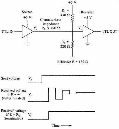
FIG. 17. Signal transmissions on a long line. The unterminated line has
reflections; proper termination solves the problem.
Line Drivers and Line Receivers
Line-termination resistors consume power. Five volts across a 150 ohm resistor requires 33 mA of current, far more than the typical logic gate output can supply.
Therefore, when terminating long lines, we usually make use of special integrated circuits called line drivers and line receivers. These chips are designed to mesh with logic signals such as TTL, and transmit and receive the signals over the long lines according to one of several accepted methods. The driver, in addition to other characteristics desirable in this application, will have sufficient drive capability to handle the extra load created by the terminating resistor.
Since the long lines often run many feet, they are especially susceptible to external noise. The noise travels toward both ends of the wire from the point of pickup. Although in a properly terminated line the noise is not reflected, it nevertheless appears as a part of the received signal. The simple line-driving technique illustrated in FIG. 19 is called single-ended and is rather susceptible to external noise. Another method, much more effective at rejecting the noise, is called differential line driving and is shown in FIG. 18. Instead of sending the signal as a voltage on one wire, referenced to ground, the differential line driver and receiver communicate over two signal wires, carrying equal voltages opposite in sign. In the differential method, it is only the signed difference in the voltages on the two wires that carries signal information, a positive difference representing an H and a negative difference being an L. If one wire picks up noise, it is likely that the other wire will pick up the same noise, since the wires are exposed to almost identical environments. Noise added to each wire has no effect on recovering the signal.
Another advantage of differential line driving is its insensitivity to differences in the ground potential at the ends of the line. Because of variations in the earth ground potential and other factors, this common-mode voltage can sometimes be many volts. Since the transmitted and received signal voltages refer to the local ground level as the zero reference point, a voltage difference between the two ground points may result in loss of information in the single-ended method.
The differential method relies solely on the voltage difference on its two wires, so differences in ground potential, which affect both wires equally, do not affect the detection of signals at the receiver.
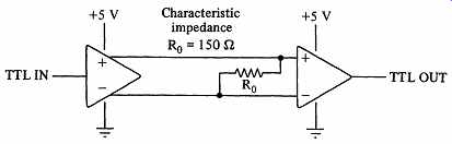
FIG. 18. Differential line driving. The lines are properly terminated
and the sign of the voltage difference on the two lines determines the logic
signal information.
Line driving and line termination are common in digital design, and often involve many signal and data lines. Groups of resistors of appropriate values are available in dual in-line packages that can be mounted in the same way as conventional SSI integrated circuits. These "resistor packs" greatly simplify the fabrication of circuits requiring terminators.
Summary
Combating noise requires careful attention to design methods and fabrication practices. We have concentrated on noise arising within the digital system itself but, as indicated in the previous section, noise from external sources such as automobile engines, transmitters, and motors can also cause problems. Our recommendations for noise abatement serve to protect against external as well as internal noise.
Here are the basic steps to minimize noise in digital circuits:
a. Use synchronous design methods.
b. Keep wires short.
c. Don't use fast integrated-circuit families.
d. Use a well-designed power supply and power-distribution system.
e. Keep wires close to the ground plane.
f. Let the wires run in random directions whenever possible.
g. Take special care with the clock line.
h. Use line-termination procedures when necessary, but avoid them wherever possible by conforming to points (b) and (c).
Noise in digital systems is a complex subject. We have touched on only its major aspects. Your best bet is to stay well within the safe area described in the recommendations.
METASTABILITY IN SEQUENTIAL CIRCUITS
In Section 4 we saw how hazards could cause a physical version of a logic circuit to produce momentary signals that were different than those predicted by Boolean algebra. To nullify the effects of these hazards, we adopted synchronous design. In Section 5 we saw that the introduction of asynchronous test inputs into an otherwise synchronous ASM could result in transition and output races.
To avoid these problems, we synchronized the asynchronous external inputs by using D flip-flops. Throughout these procedures we assumed that we are not violating the setup and hold times of the devices in the circuit. But when there are external signals that change asynchronously to our circuit, we cannot make such a guarantee. What happens when, despite our best efforts, an input transition occurs close to the active clock edge?
Realizing that the clock signal in a synchronous device can be viewed as just another input, we can broaden our question to ask what happens when two inputs to a sequential circuit change shortly before or after each other. The facts, which were not widely recognized nor even believed until recently, are disquieting.
Consider the standard D flip-flop, the 7474. FIG. 19 is the observed behavior of this device when the D-input changes about 3 nsec before the rising clock edge. The outputs of the transistors in the main feedback circuit can assume voltages that do not correspond to either of the valid digital voltage levels. This behavior is called metastability, and flip-flops exhibiting these characteristics are said to be in a metastable state. Eventually, the metastability will resolve and the flip-flop outputs will assume valid (and complementary) voltage levels, but the duration of the metastable state is indeterminate and may be quite long compared with the propagation delay listed in the data sheet.
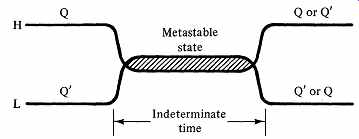
FIG. 19. Metastability in the 7474 D flip-flop. The final stable state
is unpredictable, but Q and Q' are inverses.
Other bizarre and awkward forms of metastability may occur. If the 7474's clock and D-input signals switch to high at nearly the same time, the outputs may display proper digital voltage levels with normal signal rise and fall times, but the transitions may be delayed for an indeterminate time. In an RS flip-flop constructed from cross coupled 7400 Nand Gates, the outputs may behave as shown in FIG. 20 if the gates are set or cleared by a runt pulse. In this form of metastability, which occurs in circuit families such as TTL in which signal rise times are less than the gate propagation delay, the Q and Q' outputs oscillate in-phase for an indeterminate time before resolving into valid digital voltage levels.
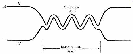
FIG. 20. Metastability in cross-coupled 7400 Nand gates. When set or
cleared with a runt pulse, the outputs may oscillate in phase.
Why do flip-flops behave this way? A gate is really an analog amplifier.
In digital circuits, the gate inputs are overdriven so that the output transistor saturates (is fully conducting or nonconducting) in its high or low state. These states form the familiar digital voltage levels. Digital logic relies on inputs passing quickly through the transition region between the voltage levels. But by judiciously biasing the inputs we can force a gate's output to be in the linear region. For instance, consider a 7404 Inverter gate driving another inverter gate:
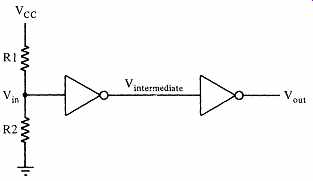
By proper choice of the resistors RI and R2, we can set the input voltage V_in such that V out = V in and V_intermediate = V in • Both inverters are in their transition region. Now, if we carefully connect the output to the input and remove the source of Vin , we will have constructed a crosscoupled flip-flop circuit that is metastable:
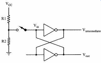
Eventually, electronic noise or the random thermal fluctuations of the atoms in the gates will upset the metastability and drive the outputs to a stable condition.
The duration of the metastable interval is unpredictable. Real flip-flops always have feedback and can always be balanced at this metastable point. There is no way to avoid this phenomenon!
How serious is this problem? If a flip-flop is in a metastable state, the probability P of still being in the metastable state after time t can be approximated by
where K and T are constants determined by experiment or calculation. The probability of remaining metastable decreases exponentially with time-a reassuring trend, but insufficient to guarantee the flip-flop's performance or to alleviate problems at fast clock rates.
To understand the effective treatment of metastability, we must gain a quantitative understanding of the timings and probabilities. At present, this information is available only from detailed experiments with devices in the various logic families. These complex experiments rely on circuits with both digital and nondigital elements to detect the existence of metastable behavior and record the frequency of metastability resulting from repeated attempts to induce the metastable condition. In the experiments, the system clock rate is fixed, and input transitions randomly distributed about the clock edge are produced at a selected rate. The usually complementary outputs of the flip-flop being tested are compared using analog comparators to detect metastability. At a specified time after the system clock transition, the result of the comparison is captured in a flip-flop. A true output, indicating metastability lingering at least as long as the sampling delay, increments a digital counter. From the count of the metastable errors that occur during the experiment, the mean time between failures (MTBF) under the given conditions can be determined.
The relationship among the experimental variables is given by

where fcp is the system clock frequency, fdata is the frequency of data transitions, at is the sampling delay, and K1 and K2 are constants describing the metastable characteristics of the device being tested. By determining the MTBF at two sampling delays, the experimenter may determine the constants K1 and K2 for the device under test.
T. J. Chaney, who has been a leader in the experimental study of metastability, has published extensive tables of K1 and K2 for many devices. For example, for the 74LS74 D Flip-flop, K1 = 0.4 sec and K2 = 0.67 nsec^-1. Consider an experiment in which the system clock rate is 10 MHz and the average rate of input transitions is 0.1 MHz. Assume we are interested in the probability of a metastable failure that endures until the next clock pulse-a measure of the reliability of a simple D flip-flop synchronizer. The calculated MTBF is several billion years. But doubling the clock frequency reduces the MTBF to only 3.7 sec! The results are extraordinarily sensitive to the clock frequency.
By running the clock slowly enough, you can obtain any degree of reliability you wish. There is a wide difference between flip-flops of the same type produced by different manufacturers and even between different batches of the same flip flop from one manufacturer. Experiments on several 74874 flip-flops running at a frequency of 25 MHz, receiving 10^5 input transitions per second, show a variation in failure rates from 2 hours to 5 x 10^31 sec. (The age of the universe is about 3 x 10^17 sec.) Push the clock speed at your own risk!
What might we do about the metastability problem?
a. We might do nothing, aside from synchronizing our external input with a D flip-flop. This method is satisfactory if we wait long enough, since the probable duration of a metastable state decreases exponentially with time.
b. We might choose a flip-flop that resolves input conflicts faster. This requires a small K2 , not just a small propagation delay. When we wish to run the clock at maximum speed and can't afford special detection circuits, such as in VLSI design, this method can be beneficial. Chaney's tables of metastability constants for standard elements can be helpful here. The Fairchild FAST series, an extension of the 74ALS series, seems to have especially good resolving characteristics. Special flip-flops constructed with tunnel diode resolvers or with ECL or gallium arsenide technologies can work at clock frequencies up to five times those suitable for standard TTL elements.
c. We might run our clock at high speed until a detector senses metastability and then freeze the clock until the metastability resolves. This method requires two tricky circuits: a system clock that can be stopped synchronously and started asynchronously and a metastability detector.
The detection circuit used in Chaney's experiments can be adapted to our purpose. In FIG. 21 we show the basis of this detector. The reference voltages V OH and V OL for the comparators correspond to the boundaries of the voltage transition region for the D flip-flop's outputs. If the flip-flop's output voltage V Q is lower than the high-level threshold and higher than the low-level threshold, the signal METASTABLE is true. This type of detector is useful with circuits in which the flip-flop output is directly available and the flip-flop does not suffer from the oscillating form of metastability. Standard metastability detectors are available for inclusion within VLSI designs.
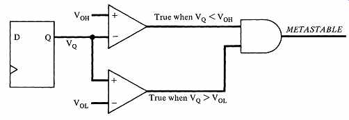
FIG. 21. A simple metastability detector.
An accepted way to form a system clock that can be stopped synchronously (the false portion of the clock is extended indefinitely) and started asynchronously begins with a delay line and an inverter in a feedback loop:
Once the circuit is properly initialized upon power-up, the delay line processes two internal states, the true and false portions of the clock signal, that travel down the line. Whenever the output CLOCK is false, the delay line is processing the next true signal through its internal storage, to emerge after the appropriate delay. Whenever the output is true, the delay line processes the next false. The waveform repeats after two delay-line time periods. We may modify this circuit to include the control signal METASTABLE in the feedback loop:
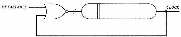
In using this circuit, the assumption is made that METASTABLE will become true only during the positive part of the clock cycle. This is reasonable for the common form of metastability detected by the circuit in FIG. 21 since, if metastability occurs, it arises soon after a clock transition. Then the positive portion of the clock cycle will run its normal course and the negative portion will be stretched by the assertion of METASTABLE. If METASTABLE becomes true during the negative phase of the clock, the impending positive phase traveling down the delay line will cause another rising edge on the clock line, defeating our intention to freeze or stretch the clock cycle in order to wait out the metastable period. Furthermore, the new positive phase will be foreshortened, and the delay line may begin to "multimode," operate at a multiple of the desired frequency.
An even number of inverters may be substituted for the delay line. Delay lines are quite stable, but they are sensitive to multimoding. Inverter chains do not have the stable delays of delay lines, but are less sensitive to multimoding.
Three potentially useful treatments of metastability were suggested above, but the technical literature is full of incorrect proposals for solving the problem.
Many of these just move the source of potential metastability from one point in the circuit to another. Here are a few treatments that do not work:
a. Using Schmitt triggers in feedback loops to clip runt pulses. If a runt pulse causes metastability in a circuit with feedback, then that same runt pulse will not cause metastability in that circuit if a Schmitt trigger is inserted in the feedback loop. However, a runt pulse of different duration and magnitude can still cause metastability in the modified circuit. This has been verified mathematically by Marinot and experimentally by Chaney.
b. Using unit distance codes so that only one state variable depends on an asynchronous qualifier. This technique can eliminate transition races in state machines, but does not address the metastability dilemma. The state flip-flop affected by the asynchronous qualifier can become metastable. The state flip-flops contribute to the production of the state machine outputs through combinational logic circuits, so metastability in a flip-flop output can have drastic consequences.
c. Using a chain of flip-flops. If a clocked flip-flop fed by an asynchronous input can become metastable, they why not feed the flip-flop output into another flip-flop to clean it up? Such a technique can indeed reduce the frequency of occurrence of metastability in the final output, but cannot eliminate it. With each flip-flop in the chain, the probability of failure decreases, yet at fast clock speeds the final probability may still be un comfortably high, and is certainly not zero.
d. Starting and stopping crystal oscillators used for clock generation. Crystal oscillators and LC resonant circuits are often used to generate precise clock frequencies. Such oscillators do not start cleanly and instantly-many cycles will pass before the oscillator's amplitude stabilizes. Therefore, an attempt to stop and restart these oscillators to stretch the clock pulse when metastability occurs will not produce satisfactory performance.
e. Gating the output of continuously running clock oscillators. "Gating the clock" was discouraged in synchronous circuits because of the possibilities of clock skew, runt pulses, and hazards. With these drawbacks, this method has little to recommend it for the treatment of metastability.
f. Using an "asynchronous arbiter." Many such complicated circuits have been proposed; all fail to solve the problem of metastability, but instead move the sensitive points to other parts of the circuit.
What Should You Do?
Metastable behavior cannot be eliminated in real circuits. The proper defenses against metastability involve lowering the probability of its occurrence, shortening its duration, or sensing its presence and freezing the action of the system until the metastable state has passed.
The simplest defense is to run your synchronous systems at moderate speeds. If you avoid pressing the system clock to the limit of your circuit, the probability of inducing metastability can be made acceptably low. As you approach a crucially fast clock speed, your circuit's behavior can deteriorate dramatically.
If running the system clock at a slow speed is not acceptable, then the next defense against metastability is to use a well-designed interruptible clock and a metastability detector. The detector will catch metastable states that manifest themselves as voltages in the transition region but will not detect the delayed-transition form of metastability.
If your clock must run fast and stretching it is intolerable, then you must investigate using flip-flops that resolve metastable states faster. At this stage, you may have to do your own experiments on metastability.
A SELECTION OF INTEGRATED CIRCUITS
The low-power Schottky families of integrated circuits are our mainstays at the MSI level of design. The popular chips are produced by several manufacturers under the standard 74LS, 74ALS, and 74F nomenclatures. In TABLE 1 we list a selection of chips that we have found useful. The table is not exhaustive, nor is it a substitute for the manufacturers' data books. We list 74LS chips, if available; many of these are also available in the improved 74ALS and 74F lines.
Some manufacturers' data books are cited at the end of the section.
TABLE 1 SELECTED INTEGRATED CIRCUITS
PREV. | NEXT
Related Articles -- Top of Page -- Home