AMAZON multi-meters discounts AMAZON oscilloscope discounts
In this section, we discuss a selection of topics pertaining to digital hardware technology. In the first three parts of this guide we emphasized the logical, functional, and organizational aspects of digital design. The design approach was top-down, with emphasis on the problem and its algorithmic and architectural solution, rather than on the details of the hardware. Of course, hardware is important; without it there would be no implementations! In this section we present some basic information about the hardware used to support digital design.
Many of the topics have a nondigital flavor to them-at least, a nonbinary flavor-being concerned with transistors, currents, power distribution, and so on. Part of our goal in this section is to give you sufficient insight into critical areas of hardware technology so that you can perceive the limitations of digital logic and can avoid wandering blindly in areas that are by nature nonlogical.
This is not a thorough course in hardware technology. We have tried to keep the number of topics and their depth of treatment to a reasonable size, and there is inevitably a certain arbitrariness in our choice. The Readings and Sources give sources of additional information.
ON TRANSISTORS AND GATES
Semiconductors form the basis of the electronic revolution and are the primary components of our circuits, so we will sketch some of their properties as background for the topics discussed in this section.
The Flow of Electrical Charge
The conduction of electricity is the result of charged particles moving from one place to another. In a flashlight, electrons leave the negative battery terminal, flow through the flashlight case, through a wire (the light-bulb filament), and back into the positive battery terminal. Here the charged particles are negative electrons.
When experiments on electrical conduction were first performed, electrons had not been discovered. The early workers guessed that the carriers were positively charged, and the convention of positive current remains with us today.
Therefore, we draw arrows for the flow of charge from the positive battery terminal to the negative, just the opposite of the electron flow. This causes no real difficulty. The gain in clarity is not worth the chaos that would result from changing conventions. Therefore, all current arrows on diodes, transistors, and other electronic devices refer to positive current.
Metallic Conduction
In metals the mobile particles are electrons that have been stripped from the metal's atoms and are free to roam throughout the metal. The electrons act much like a gas of negative electricity trapped within the metal by the positively charged metal ions formed when the electrons left the neutral atoms. Compared with the electrons, these positive ions are massive chunks of matter, locked into a regular geometric pattern called a crystal lattice. It is this locked pattern that gives metals their strength. The free electrons contribute to metallic properties such as high thermal and electrical conductivity, and cause the bright, shiny appearance characteristic of metals.
Insulators
Insulators have no free electrons; all the electrons are locked up in the chemical bonds tying the atoms of the insulator together. The firmer the bonds, the better the insulator. These bonds are also responsible for the characteristic brittleness of insulators.
Semiconductors
Semiconductors are fundamentally insulators with a tiny proportion of broken chemical bonds. The bonds are broken by thermal vibrations. The vibrations set free electrons that form a gas which can then conduct electricity just as in a metal. The resulting gas is billions of times more dilute than in a metal, and semiconductors are correspondingly poor conductors. The most common semi conductor is silicon, which has four electrons available for bonding to other silicon atoms. The resulting crystal structure is a tetrahedral arrangement with each silicon atom bonded to four others.
Interesting things happen when a phosphorus atom with five bonding electrons is placed in the silicon crystal. The phosphorus atom adapts as best it can by using four electrons to bond with surrounding silicon atoms, and releases the fifth electron to migrate throughout the crystal. This electron is in addition to those few that are set free by thermally broken silicon bonds. Now we have a way to control the number of free electrons in the crystal, by deliberately introducing phosphorus as an impurity. Since the resulting charge carriers are negative, we call the "doped" crystal an n-type conductor.
But we may play the game with boron atoms instead of phosphorus. Boron has only three electrons available for bonding. When placed into a silicon crystal, a boron atom tries to get four electrons so it can look like its silicon neighbors.
It does this by robbing an electron from a neighboring silicon atom, which then has only three electrons. This electron-deficient silicon atom may then steal an electron from a neighbor. The deficiency is called a hole, and it acts like a mobile positive charge; the result is call1ed a p-type semiconductor.
Our present-day digital technology is built on the precise creation of adjacent chunks of p- and n-type silicon. The boundary between the p and n regions is called a p,n junction. In many cases, useful electronic properties arise at the p,n junction, so we will discuss some of the devices that can be built from junctions.
Diodes
The diode will pass current easily in one direction but block it in the opposite direction. The symbol has an arrow showing the direction of positive charge flow. The diode is constructed of a tiny chip of silicon with a single p,n junction as follows:
Diode symbol Construction
A diode is forward-biased when the voltage at the output end (the direction of the arrow) is more negative than at the input, thus causing the diode to pass current. When the output voltage is positive with respect to the input, no charge flows, and the diode is reverse-biased:
Forward biased (charge flows~)
Reverse biased (no charge flow)
Bipolar Transistors
Bipolar devices are three-layer sandwiches that come in two forms-pnp and npn. As shown below, the pnp transistor has an n layer sandwiched between two players; npn has the reverse arrangement. The term bipolar arises because conduction involves both p- and n-type charge carriers. The following figure shows the construction and symbol of each type:
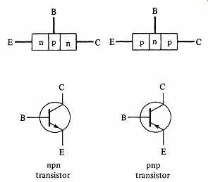
As always, the arrow shows the direction of positive current. In both types of transistor, the major current is between the emitter (E) and the collector (C). In a pnp transistor, the charge carriers are p-type holes; electrons are the carriers in the npn transistor. In both types, the charge must pass through a thin layer called the base (B), of opposite semiconductor type. The base can modulate (control) the emitter-collector current by increasing or decreasing the density of its charges. Changing the voltage on the base lead accomplishes this modulation.
Supplying operation power. The arrow in the transistor symbol is the key to biasing the power supply properly. The arrow points in the direction of positive current, so we must have these arrangements:
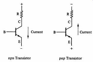
In each case the resistor R limits the current whenever the transistor is conducting; without the resistor, the transistor could be damaged. Most bipolar digital circuits are made with npn transistors. The positive supply voltage in these circuits is called Vcc.
Turning on and off. In digital work the conducting path between emitter and collector is in one of two states, conducting or nonconducting. In the nonconducting, or off, state no current is flowing, whereas in the conducting,
or on, state there is almost a short circuit between emitter and collector. We may think of the transistor as a small switch that can be flipped between open and closed positions. The analogy with a switch gives rise to the common name for a transistor used in digital work: the switching transistor.
The base lead controls the opening and closing of the switch in the following way. If we bias the base to inject current in the same direction as the emitter arrow, the transistor switch will turn on. For example:
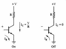
On Off The transistor acts as an amplifier of current, in that a small base current can control a much larger current in the emitter-collector path. The term ..:lIe/ ..:lIB defines the gain of the transistor; in common switching transistors, the gain is from 20 to 100. In an npn transistor, current will begin to flow in the base lead when it is 0.7 V more positive than the emitter. A pnp transistor will turn on when the base is 0.7 V more negative than the emitter.
MOS Transistors
The MOS (metal oxide semiconductor) transistor is a unipolar device-its conduction mechanism depends only on charge carriers of one type. The MOS transistor was proposed before the bipolar transistor, but technological difficulties slowed its development until the need for smaller cells in memory chips caused sufficient attention to be focused on the fabrication process.
Consider a bar of p-type silicon with two n-type regions, source and drain, diffused into its surface:
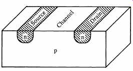
The p-type region between the n-type diffusions is called the channel. This arrangement appears similar to the bipolar npn transistor, except that the channel is several microns wide-much wider than the base region in a bipolar transistor.
Conductive electrodes, usually made of aluminum, are attached to the source and the drain, and are biased with the drain positive with respect to the source.
The channel-drain junction is not forward-biased, so no current flows across the channel through the transistor. Now place a third electrode-the gate-over the channel, separated from the channel by a thin insulating layer of silicon dioxide.
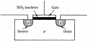
The gate and channel form a capacitor. The mobile carriers in the channel are positively charged holes. If the gate is unbiased or negatively biased with respect to the channel, the holes dominate in the channel, and no current can flow between the source and drain. If the gate is made positive with respect to the channel, electrons will be attracted to the channel region. With sufficient positive gate bias, enough electrons will be available to overcome the holes in a thin region of the channel adjacent to the insulating layer. The induced negative charge carriers form a conducting path from source to drain, allowing a current to flow across the transistor. A portion of the channel is temporarily converted from p-type to n-type. This is the principle of operation of the unipolar n-MOS transistor.
Such a device is an enhancement-mode transistor, since biasing the gate enhances the concentration of the (n-type) charge carriers. It is also possible to fabricate depletion-mode n-MOS transistors, in which biasing the gate depletes the charge carriers. During fabrication of a depletion-mode n-MOS transistor, a thin layer under the gate is diffused with n-type impurities. Like the enhancement mode transistor, the drain is biased positive with respect to the source. When the gate is unbiased (or positively biased), the transistor conducts current from the source to the drain across the n-type channel. When the gate is biased negatively, positive charge carriers are attracted into the n-type channel region until the n carriers are neutralized. Conduction across the channel ceases, and the transistor turns off.
The n-MOS transistors have negative charge carriers. MOS transistors with positive charge carriers may be constructed by forming a p-type source and drain on the surface of an n-type substrate. Such p-MOS transistors exist in enhancement mode and depletion-mode types.
Several notations are used for representing MOS transistors. The preferred notation is a circle on the gate input of a p-MOS transistor and no circle on the n-MOS transistor.
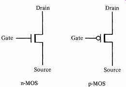
The drain voltage is V DD; the source voltage is V ss. Typical n-MOS supply voltages are 0 volts for V ss and 5 volts for V DD' In good mixed-logic style, the circle shows that a low gate-voltage turns on the p-MOS transistor. In circuits that are entirely of one type of transistor, the distinguishing notations are often omitted.
Gates from Transistors
An inverter. Consider the bipolar transistor circuit of FIG. 1. Resistors R) and R2 limit the flow of current in the base and collector leads. As the input voltage IN rises above 0.7 V, current will begin to flow in the base, the switch will close, and the emitter-collector path will approach a short circuit. The output will then be at ground voltage, so we see that an H input will yield an L output.
As we reduce the voltage at input IN to below 0.7 V, current will cease to flow in the base, and the emitter-collector path will open. With the switch open, little current flows through R2, so the voltage at the output OUT is high. Thus an L input yields an H output, just the behavior of an inverter.
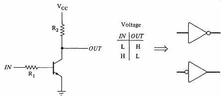
FIG. 1. An npn transistor used as an inverter.
A two-input gate. Connect two transistors to a common collector resistor as shown in FIG. 2. If either or both transistors are on, the output will be shorted to ground, and the OUT voltage will be low. If both transistors are off (both switches open), the collector resistor R2 can pull the output voltage high.
The voltage table follows directly from this behavior, and the logic symbols result from routine applications of mixed logic. This circuit is the basis of bipolar gate construction. Actual commercial gates are more complex, in order to achieve various advantages of speed, power, and stability. Similar logic gates arise from MOS technology. For instance, FIG. 3 shows an inverter and a Nand gate made using n-MOS transistors.
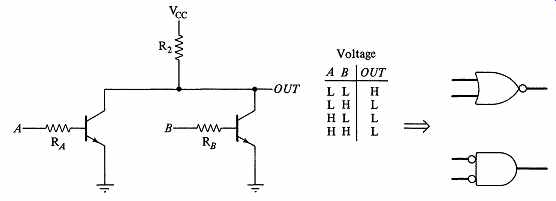
FIG. 2. A 2-input gate made from two transistors.
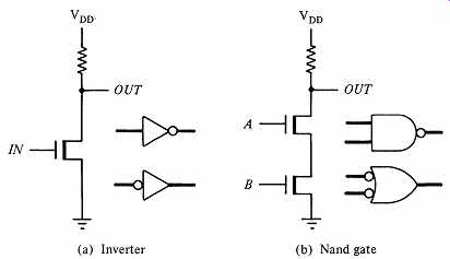
FIG. 3. n-Mos logic gates.
BIPOLAR LOGIC FAMILIES
RTL: Resistor-Transistor Logic
How transistors interconnect to form gates determines the type of integrated circuit logic, or logic family. The bipolar transistor arrangements in the previous section were used in an early family called RTL, which was simple to make but was sensitive to noise and had longer propagation delays on the L ~ H transition than on the H ~ L transition. When the output transistor turned on, there was a sudden low impedance to ground, which rapidly discharged stray capacitance, so the H ~ L transitions were fast. When the transistor switched off, resistor R2 had to charge up the stray capacitance, which took much longer. RTL soon gave way to DTL (diode-transistor logic), which in turn was supplanted by TTL.
TTL: Transistor-Transistor Logic
To make propagation times more symmetric, the output driver must have a low impedance path to Vcc as well as to ground. This requirement resulted in the "totem pole" configuration of two output driver transistors, one to pull the output high and the other to pull it low; see FIG. 4. Here R is small, so it can charge and discharge stray capacitance on the output line rapidly. To produce an H output, transistor G must be on and G' off. An L output requires G to be off and G' on. The control signals G and G' are the complements of each other.
A totem pole output stage, providing solid pull-up to Vcc and solid pull down to ground, is common in modern logic families. However, the configuration has two problems:
a. Current spikes. It is hard to switch one of the totem pole transistors off before the other comes on. There is an overlap of a few nanoseconds when both are on, and during this time the power supply is shorted to ground, except for the small resistance R. This puts a sudden short load on the power supply-a spike-which in turn can affect other gates. TTL circuits require good power supply and distribution of power to alleviate this problem.
b. Output fights. One transistor in each totem pole is always on. Suppose you inadvertently tie two totem pole outputs together. If one circuit is trying to produce an L and the other an H, the two circuits provide a low impedance path from Vcc to ground through the two turned-on transistors.
In this case, the output voltage is indeterminate, and things will get hot! TTL logic families. TTL is a well-developed line of integrated circuits, with many subfamilies. Some of the subfamilies, such as the 74Lxx and 74Hxx series, are obsolete, and we will not discuss them. Here is a brief summary of the most important TTL subfamilies:
a. 74xx series: regular TTL. This is the oldest TTL line, still found in some old systems. It was fairly fast but drew considerable power.
b. 74Sxx series: Schottky TTL. This is the fastest TTL line, but it requires high power and suffers from severe noise problems because of its fast switching speed. Its use requires close attention to power distribution, wire length, and power supply bypassing.
c. 74LSxx series: low-power Schottky TTL. This is a fairly fast series, with low power requirements. It was the predecessor to the improved series described below. Its speed is slow enough to permit standard wiring practices.
d. 74ALSxx series: advanced low-power Schottky TTL. Twice as fast as 74LSxx but consumes half the power. A good choice for new designs.
e. 74Fxx series: Fairchild's advanced low-power Schottky TTL ("FAST"). Three times as fast as 74LSxx (and therefore faster than 74ALSxx) but requires nearly three times the power of 74LSxx. A good choice when speed is important.
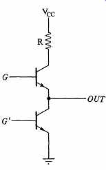
FIG. 4. The TTL totem pole output configuration. The internal signals
G and G' are complements of each other.
Schottky technology. Most digital circuits drive their switching transistors fully on and fully off, a switching mode called saturation. Such devices tend to be rugged, simple, and inexpensive, but slower than circuits that do not saturate their transistors. Consider an npn transistor: When the base voltage becomes sufficiently high, the transistor is conducting enough to establish a valid TTL output level. Further increases in the base voltage serve only to force more charge into the base until the transistor is saturated, without improving the logical capabilities of the device. When the base voltage drops, the transistor shuts off, but not before the accumulated charge on the base has bled off. The time required to bleed off the base charge is called storage time; to achieve high speed, the storage time must be reduced.
Saturation can be avoided by clamping the circuit's inputs with Schottky diodes to prevent unnecessary upward excursions of base voltages. The resulting speedup is substantial. Nearly all newer TTL devices use this technique. Chip designers have used the extra speed in two ways, illustrated by the 74S and 74LS series. In general, transistors will switch faster at higher power levels. In 74S, the original Schottky series, the power consumption is about double that of regular TTL, but the speed is three times as great. In 74LS, the designers reduced the power consumption to one-fifth that of 74S, to give a family with the same speed as regular TTL. Subsequent improvements of74LS have resulted in several TTL series that consume even less power, and have greater speeds.
The internal structure of modern TTL devices is quite complex, but the newer series provide rugged, economical chips that are the workhorses of the digital industry.
ECL: Emitter-Coupled logic
ECL is the fastest logic line in common use. It takes advantage of the increase in speed attained by operating transistors in the unsaturated mode. An ECL circuit contains a differential amplifier (an amplifier whose output is a function of the difference between two input voltages) that compares a logic input with a reference voltage. The result is used to steer a constant current into one of two paths without saturating the circuit's transistors. The output circuit always contains two paths that have complementary voltages, thus providing easy access to high- and low-active versions of the output logic variable.
ECL circuits have gate propagation delays of about 1 nsec, and EeL flip flops can be toggled at a rate of 500 MHz-several times faster than their nearest competitor, 74S TTL.
ECL has several advantages for designers:
a. Since the current is nearly constant, even during switching, EeL circuits do not tend to cause current spikes on the power supply. This property simplifies the distribution of power to the EeL design-an important advantage since power distribution tends to become troublesome with faster logic lines. Yet EeL is the fastest of all.
b. ECL outputs are available in .H and .L forms, with equal propagation delays. This virtually eliminates the need for voltage inverters.
c. The complementary outputs are excellent for use as line drivers.
d. In the most convenient ECL family, the rise time of the gate outputs is purposely made slower than the internal propagation delay. This simplifies the clocking of synchronous circuits and greatly reduces electrical crosstalk.
e. The slowed rise times permit the use of ECL in properly designed wire wrapped circuits.
f. ECL outputs may be directly connected, to achieve a wired-OR or wired AND logic function.
g. Power supply current is independent of the system clock rate. This enhances EeL's role as a high-speed logic family. In most logic families, the power supply current increases with clock speed.
Offsetting these advantages are several serious disadvantages of ECL:
a. Although power consumption is nearly independent of clock speed, ECL is a "power hog."
b. The high speed and fast rise time of signals in ECL circuits makes the propagation delay along circuit interconnections a significant factor in the design. To achieve reliable performance, one must frequently use trans mission-line techniques to inhibit signal reflections.
Manufacturers have made ingenious modifications and compromises in EeL products to ease the problems brought on by their blinding speed, and EeL is a reasonable choice when speed is essential. However, using EeL in a design requires much more care than a slower family such as 74LS TTL, so EeL is not the first choice for the design of many circuits.
UNIPOLAR LOGIC FAMILIES
MOS technology provides the basis for several unipolar logic lines. All have the advantages of a small unit area and low power consumption and the disadvantages of sensitivity to damage from static charge and of relatively slow speed.
p-MOS and n-MOS Logic
MOS technology is popular for large, complex digital systems because the basic MOS gate is much smaller than its bipolar counterpart. Since less power is consumed, the problem of heat dissipation is more manageable than in bipolar technology. Nearly all dynamic memories and most microprocessors are made with n-MOS technology. The p-MOS technology is little used today, except as a component of complementary MOS (CMOS) circuits.
CMOS: Complementary MOS Logic
CMOS is a logic family that uses both n-MOS and p-MOS transistors to produce a circuit that consumes much less power than either alone. Low power consumption is obviously desirable for such lightweight and portable devices as watches and pocket calculators, and it is also necessary if the packing density of transistors on chips is to increase. Power generates heat, which must be dissipated efficiently to keep the device's temperature within reliable working limits.
To understand CMOS operation, consider the simple bipolar and unipolar inverters shown in Figs. 1 and 3. These inverters consume power whenever the transistor switch is conducting, because current flows between power and ground through the main output pull-up resistor. When the transistor switch is not conducting, only a small current flows across the resistor. The resistor provides a means of establishing the high voltage level when the transistor is not conducting, and limits the current flowing through the transistor when the transistor is conducting. In CMOS, both these functions of the resistor are provided by a p-MOS transistor whose operation is complementary to the usual n-MOS output transistor:
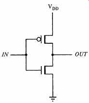
In this arrangement, one transistor is conducting whenever the other is shut off.
When IN is a high voltage, the n-MOS transistor is on and the p-MOS transistor is off, producing a low voltage level at the output OUT. When IN is a low voltage, the n-MOS transistor is off and the p-MOS transistor is on, producing a high voltage level at OUT. Except during the brief instant of switching, no
current flows between V DD and V ss. The input IN and the destinations for OUT, connected only to the capacitative gate of MOS transistors, have no steady-state currents. Therefore, the power consumption of the CMOS gate is extremely small. The CMOS cell is nearly as small as in noMOS. Whereas earlier CMOS integrated circuits were slow, the newer Hi-Speed CMOS family rivals TTL in speed while retaining the extremely low power consumption of the earlier CMOS devices. CMOS is popular in VLSI and is also available as pin-compatible counterparts to 74LS-series SSI, MSI, and LSI components. One may develop a circuit using the rugged 74LS chips and then substitute the less-robust CMOS equivalents to drastically reduce the power consumption.
THREE-STATE AND OPEN-COLLECTOR OUTPUTS
Open-Collector Outputs
The TTL open-collector circuit is essentially a switching transistor without an internal connection to Vcc: the collector is open. To complete the circuit, we must supply a connection from the open-collector output to Vcc, through a suitable external resistor. Here is the circuit for an open-collector inverter, with one commonly used circuit symbol:
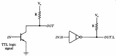
The supply voltage V + may vary over a wide range, and we must choose the resistor R to suit the requirements of the circuit. Since the open-collector circuit does not use a totem pole configuration, it is slower than its other TTL counterparts.
Various chips in the 74 and 74LS lines are available with open-collector outputs, including inverters and various gates that perform AND and OR logic. We use the vertical line within the gate symbol to designate open-collector output; there is no universal standard notation.
There are two main uses of open-collector gates:
Buffer-Driver. Whereas the normal open-collector chip has current behavior similar to its parent 74 or 74LS family, it is possible to build an open-collector current buffer that can accept much higher currents than the ordinary variety.
This, coupled with the ability to set V + at any reasonable level, makes the open collector useful for driving display lamps and other devices with non-TTL voltage requirements or with high current demands; see the later section on lamp driving for more details.
Wired OR. Suppose we tie the outputs of several open-collector gates together, and power them all from V + through a single resistor, as in Fig. 5. In this circuit, if any open-collector transistor is on, the output will be L. For a transistor to be on, its base must be H, so we observe the voltage behavior shown in the figure. This voltage table corresponds to an AND or OR logic operation, depending on the voltage convention we select. Since we achieve this logic operation without an actual AND or OR gate, we speak of a "wired OR" or a "wired AND." The rule is:
Wired OR if T L.
Wired AND if T H.
The wired OR has some uses in bussing and interfacing, but it appears more attractive than it turns out to be in practice. The circuit is spread over several packages. Suppose it doesn't work: which package is bad? This alone is sufficient cause for caution. Another minor problem is that now we have to put an external resistor into the circuit, which is awkward packaging. Still a third objection is the open collector's slow speed. The open collector has its place, but as a logic tool it is not popular with designers; the three-state output has largely eliminated the need for it as an implementer of logic. Sections 2 and 3 have additional discussions of open-collector circuits.
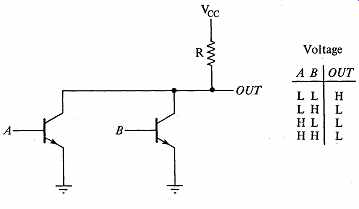
FIG. 5. An open-collector wired OR.
Open-collector resistor value. The open-collector pull-up resistor R must be within a certain range for proper operation. We will demonstrate a computation of R for a wired OR circuit. In this case, where we must produce a TTL compatible logic signal as output, V + will be equal to Vcc, namely, 5 V. Assume that we have six ordinary 74LS open-collector outputs wired together, with the wired output feeding four 74LS inputs. We must consult the data sheets for the information needed for the computations. A 74LS open-collector output can safely pass only a certain amount of current, at most 8 mA. This maximum current could occur when the transistor is on and the voltage at the output is close to zero. We must make certain that the total current that can flow through the transistor is less than its maximum rating. This current comes from two sources: through the resistor, and from each input tied to the open-collector output. Each 74LS input may provide as much as 0.4 mA in the low state. The current allowed through R is the difference of the maximum open-collector current (8 mA) and the total current from the inputs. The computation is
E 5 - 0 Rmin = I = 0.008 _ 4 x 0.0004 = 780 0
We may determine the maximum R from the number of inputs and outputs attached to the output line. Low-power Schottky gates will treat an input voltage of 2.0 V or greater as a high level, and we must make sure that the voltage drop across R is not so great that the actual high-level voltage of the output drops below 2.0 V. Each 74LS input draws as much as 20 p.,A in the H state, and each 74LS open-collector output will draw 100 p.,A (into the output). All of this current must come from V cc through R, so
5 - 2 Rmax = 6 x 0.0001 + 4 x 0.00002 = 44000
One more consideration: the resistor must be of sufficient wattage to dissipate the power generated in it. Power is P = E x I. Using Ohm's Law, we may write R = E2 jP. The maximum power loss in the resistor occurs when the voltage drop is greatest, about 5 V. If we wish to use a V4-watt resistor, the minimum safe value of R is
52 Rpower min = 0.25 = 100 0
This value is much lower than the earlier minimum of 780 0, so our 1/4-watt resistor will be quite sufficient for any proper value of R. From these computations we see that a value of 1000 to 2000 0 is safe.
More details will be found in manufacturers' data books.
Three-State Outputs
Many chips in the major integrated circuit families have three-state outputs. In addition to the normal Hand L output states, a three-state gate has a third state Z, called the high-impedance state. When the gate is in the high-impedance state, the chip's output is effectively disconnected from the circuit. In addition to its normal inputs, a three-state chip also has a control input called the three state enable, whose purpose is to select between normal (enabled) and high impedance (disabled) modes.
Using TTL As a model, we may show how the high-impedance state comes about. In the normal TTL totem pole output stage, one of the two totem pole transistors is always on, so there is always a relatively low-impedance path through the totem pole. The three-state circuit permits the control input to turn both totem pole transistors off when the control is false. Schematically, the output circuit is as in FIG. 6. When the three-state signal is false, the outputs of the ANDs are both low, and both totem pole transistors are off. In this case, the current in the output circuit has no low-impedance path and the output behaves as if the gate were not attached.
As long as we make sure that at most one three-state element is enabled at a time, we may tie many such outputs together. This property has had a great, almost revolutionary, effect on data bus design, where we wish to wire all data sources onto the bus and allow at most one to "talk. " (See the discussion in Section 3.)
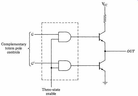
FIG. 6. A model of TIL three-state output control.
INTEGRATED CIRCUIT DATA SHEETS
The integrated circuit data sheet is the document that defines a given device. It contains much important information, some unique to the device, and some fairly standard for the logic family. There is no standard format for data sheets, although some of the terminology is uniform among manufacturers. In a typical data sheet for a digital device, we expect to find:
a. The chip's name and number and a description of its major characteristics.
b. A logic symbol of the manufacturer's choosing, naming the functions of each input and output of the chip.
c. A pin diagram, showing the function associated with each pin.
d. A complete description of the use of the chip, often with a detailed voltage table. For SSI chips, this description can be quite brief; for MSI and LSI, it can be complex. For VLSI, the description may require dozens of pages.
e. Electrical and environmental specifications for the chip's operation.
f. For MSI, LSI, and VLSI circuits, perhaps some information about applications.
Electrical Data
The electrical information is the most difficult part of the data sheet to master, but it is important that you understand some of the details. Fortunately, the terminology is nearly standard, and for TTL many of the values of the parameters are standard, although the exact form of presenting the information varies. The following discussion applies to the low-power Schottky TTL family. Other logic families have different values of parameters, but the treatment is similar.
The data sheet will usually describe two versions of a chip, a military grade and a commercial grade. The military grade is designed to operate over a wider temperature range than the commercial grade and will have slightly different operating characteristics. Manufacturers differ in how they specify these grades, but most manufacturers use the prefix "74" for the commercial grade and "54" for the military grade. We will discuss the commercial grade.
Standard nomenclature is V for voltage, I for current, and subscripts I for input, a for output, H for high voltage level, and L for low voltage level. Thus V OL stands for low-level output voltage. Hand L represent the binary voltage levels; the electrical data will specify the actual range of voltages for these levels.
The electrical information falls into three categories: operating conditions, static operating characteristics, and switching data.
Operating conditions. These are the basic conditions under which the manufacturer states that the chip will perform as specified. The usual parameters are:
Temperature: 0° to 75°C for commercial-grade chips; - 55° to 125°C for military grade.
Vcc: supply voltage. For all commercial TTL chips, the allowable range is 4.75 to 5.25 V, with a typical value of 5.0 V.
IOH: high-level output current. IOH must not exceed the stated value, which for 74LS is typically 400 /LA, directed out of the output.
IOL: low-level output current. This is the maximum allowable current through the output in the low level. For 74LS, the usual value is 8 mA, directed into the output.
Static characteristics. The static, or dc, electrical characteristics describe how the chip's outputs and inputs will react to specified stable operating conditions.
The major parameters are:
VIH : high-level input voltage. This is the minimum voltage that the chip guarantees to recognize as a high signal level. For 74LS, this is 2.0 V. The chip will treat any input voltage from 2 to 5 V as H.
VIL : low-level input voltage. This is the maximum voltage that the chip guarantees to recognize as a low signal level. For 74LS, this is 0.8 V, so the chip accepts an input between 0 and 0.8 V as an L. An input voltage between VIL and VIH is in the forbidden region, and the manufacturer does not guarantee reliable performance.
VOH: high-level output voltage. If the output-high current IOH does not exceed its maximum rating (given in the operating conditions), then VOH represents the voltage that the chip will produce for a high signal level.
Usually, the data sheet will give a guaranteed minimum VOH (2.7 V for 74LS) and a typical VOH (usually 3.4 V for 74LS). VOL: low-level output voltage. This is the low-level counterpart of VOH. If IOL does not exceed its maximum rating, then VOL represents the voltage that the chip will produce for a low signal level. The guaranteed maximum value of this voltage for 74LS is 0.5 V. The typical low-level output voltage for 74LS is usually 0.25 V.
IIH: high-level input current. This is the current that an input will draw when presented with a high voltage level. The data sheet gives a maximum value, which for 74LS is 20 u-A at 2.7 V. The direction of this current is into the input, and the value is a function of VIH . The higher the voltage on the input, the higher is the current demanded by the input.
ILL: low-level input current. This is the current that an input will require when presented with a low voltage level. For 74LS, the maximum value of ILL is 0.4 mA at 0.4 V; the direction is out of the input. The lower the voltage on the input, the higher is the current.
Icc: supply current. This is a measure of the chip's power consumption.
The data sheet will specify the operating conditions under which the supply current is measured and will usually give a typical and a maximum value for Icc. The supply current varies greatly with the chip type; the information is useful when estimating the size of the power supply needed for a given circuit.
Switching characteristics. The switching, or ac, characteristics show the time dependence of various transitions in the chip. The most fundamental switching parameter is the propagation delay, which is the elapsed time from the initiation of an action until the outputs reflect the result of the action.
In the usual notation, tpLH is the propagation delay of an output going from L to H; tpHL is the counterpart for an output going from H to L. In combinational circuits, the delay period starts with a change in an input. For complex circuits, either combinational or sequential, having several types of inputs and outputs, the data sheet may list several propagation delays. Propagation delay information usually has maximum and typical values. For simple 74LS gates, propagation delays are about 5 nsec; more complex circuits may have delays of a few tens of nanoseconds.
Sequential circuits have another class of switching information in the data sheet: the setup and hold times. Setup is the time prior to some event (such as a clock edge) during which an input must be stable to assure reliable device operation. Hold time is how long after an event the input must remain stable.
Setup and hold times are usually stated as minimum and typical times. Setup times for 74LS vary considerably but range up to about 30 nsec, with 15 or 20 nsec being typical. Generally, we like the hold times for inputs relative to the clock to be no greater than zero. The minimum setup and hold times listed in the data sheet are conservative values. If you meet these conditions, all chips of that type should work. The "typical" entries for setup and hold times are usually considerably smaller than the "minimum"; the typical chip will be faster than the slowest chip, to which the minimum values apply. It is not easy to tell, so it is best to stick with the conservative specifications.
PERFORMANCE PARAMETERS OF INTEGRATED-CIRCUIT FAMILIES
Loadings, noise margins, and propagation delays are given in integrated circuit data sheets or may be inferred from data sheet information. During the implementation phase of a project, the designer must take care to avoid violating the manufacturer's specifications. Here we discuss these design parameters and compare the TTL-compatible integrated circuit families.
Input and Output Loadings
Consider a wire representing a signal path from an output to one or more inputs.
Every input on the wire places a current load on the signal source; the data sheet specifications IIH and IlL characterize the load. The output of an integrated circuit is capable of handling only a specified maximum current before the quality of its signal deteriorates; we measure the output drive capability by the data sheet specifications IOH and IoL . Each family of integrated circuits is designed around standard values of these four specifications of current; if the standard specifications of output current are not exceeded, the "standard gate" will perform correctly within the standard input current limits. The standard IIH and IlL values are called the unit load for the high and low logic levels. In most cases, inputs draw one unit load. Sometimes, when an input goes directly to several gates within the device, the input will draw two, three, or more unit loads. Familiarity with the concept of unit load will help you to interpret the specifications in the data sheet.
The ratio IOH/IIH of the standard values is called the fanout of the high voltage level; similarly, the ratio IodIIL is the fanout of the low voltage level.
For a given family of integrated circuits, fanout describes how many standard inputs a standard output will drive. Designers use fanout as a rule of thumb to avoid overloading circuit outputs with too many inputs. For most families the fanout values for high and low voltage levels are the same; when they differ, we use the smaller value.
The TTL-compatible integrated circuit families have the current behavior shown in the accompanying table. A 74ALS standard output will drive 20 standard 74ALS loads, and a Hi-Speed CMOS standard output will drive 50 standard Hi Speed CMOS loads. The output drive capability of integrated circuits is well standardized. However, since inputs may use several unit loads, you must do more than simply count inputs; you must check the data sheets for each chip.
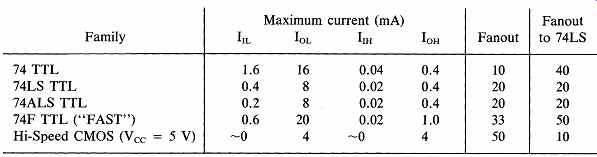
When using chips from different families within a circuit, you must compute the loading of each output, using the actual inputs attached to the output. The table shows the fanout of each family into inputs of the same family, and also the fanout of each family into 74LS inputs. From the current data in the table you can compute the fanouts of any family into any other family by using the appropriate standard input and output currents. The mixing of "compatible" integrated-circuit families requires close attention to the loadings. In the course of constructing or debugging a circuit, it is easy to insert a 74F chip in place of a 74ALS chip without bothering about the possible consequences. You gain additional drive capability at the 74F output, but the inputs to the 74F chip require more current than the 74ALS chip and you may be overloading earlier outputs by making this exchange.
Handling overloaded outputs. The drive capability of modern logic chips is usually sufficient to handle the input loadings, but occasionally you will have to drive more loads than the output will handle. One solution to this problem is to split the inputs into groups and form an identical output to drive each group. For example:
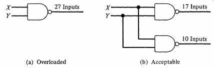
Another technique is to use a high-power amplifier called a buffer to drive the entire set of inputs. For instance, in a 74LS37 Quad Two-Input Nand Buffer IOH = 1.2 mA and IOL = 24 mA, three times the values of the standard 74LS gate output.
As you design a complex circuit, you must watch out for overloading. An undetected overload can pull your signal into the forbidden voltage region, producing unreliable performance which may be hard to diagnose.
Noise Margins
For each integrated circuit family, the allowable voltage ranges of valid high and low levels are rigidly defined. Inputs will accept a wider range of voltages than outputs produce. This is necessary because signals inevitably undergo deterioration between the source (an output) and the destinations (inputs). For each voltage level, the difference between what the input will tolerate and what the output is guaranteed to produce is called the noise margin.
The low-level noise margin is…
The high-level noise margin is…
These figures represent how much deterioration a signal may suffer in going from an output to an input before the voltage enters the forbidden region between the levels, where it is no longer recognizable as a valid digital signal level. High noise margins are desirable. The accompanying table shows the standard voltage limits and derived noise margins of the TTL-compatible integrated circuit families.

CMOS can operate within a range of power supply voltages; our figures assume the use of the normal TTL power supply voltage of 5 V. Hi-Speed CMOS has excellent noise margins, so inputs are less affected by noise than with the other families. (On the other hand, CMOS is much more sensitive to damage from static electric charge than TTL, and must be handled with care.) Noise margins are an important figure of merit for an integrated circuit family, since noise, whether introduced by circuit losses or from external sources, is a fact of life in digital equipment. Imagine the difficulty we would be in if the noise margins were zero!
UNUSED GATE INPUTS
Logic chips frequently have unused inputs. Gates often have too many inputs (e.g., when a 74LSOO Nand gate is used as an inverter) and so do flip-flops and registers having asynchronous set and clear inputs. Here are some procedures for neutralizing these unneeded inputs.
To force a high voltage level on an unused input: for 74 TTL, connect the input to Y cc through a 1-kOhm resistor; for 74LS, 74ALS, and 74F TTL and for CMOS, connect the input directly to Y cc.
To force a low voltage level on an unused input: connect the input directly to ground.
For unused AND and OR gate inputs, another option is available for standard 74 TTL: connect the unused input to a used input on the same gate. This is equivalent to an application of the Boolean algebraic identities A· A == A + A == A. Because it makes the chips more sensitive to noise, this method should not be used with low-power Schottky or CMOS integrated circuits.
In the TTL families, an unattached (floating) input tends to assume a high voltage level, and it is tempting to just let the input float to achieve an H. Don't do it! The floating input acts like a small antenna and can easily pick up sufficient noise from the surroundings to cause spurious behavior. Always establish a firm value for unused inputs.
THE SCHMITT TRIGGER
The Schmitt trigger is an ordinary inverter with a little bit of internal feedback.
The amount of feedback is chosen so that the circuit is not yet a flip-flop, but has some flip-flop characteristics superimposed on normal inverter behavior.
Figuratively, it takes a big push to switch the output, but once switched it will stay there even if the push is partially relaxed.
FIG. 7 describes the behavior of the Schmitt trigger's input and output voltages. If we start with V_in = 0, the output is H as with a normal inverter (point A). Now increase the input voltage from 0 toward Y. The output will remain H, on path A ~ B. Increase V_in a little more, and the output will switch suddenly to L at V_in = Y, and will remain L as the input voltage undergoes limited excursions around Y (between points E and D). Now decrease V_in' The output will not switch until V_in is considerably less than Y. In fact, we will have to lower Vin all the way to X (point F) before Vout will switch to H.
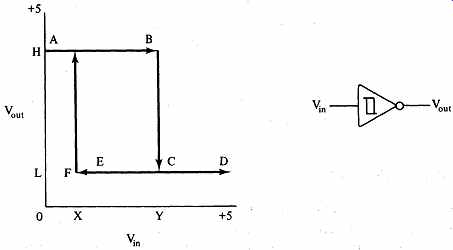
FIG. 7. Voltage behavior and symbol of the Schmitt trigger.
It is this different switching point on increasing and decreasing voltage that gives the Schmitt trigger its utility. The action, called hysteresis, is measured by the difference between the X and Y voltages. The Schmitt trigger circuit symbol is a standard inverter with a hysteresis curve drawn inside the triangle, as shown in FIG. 7. For a TTL Schmitt trigger, typical values for X and Y are 0.8 and 1.6 V, respectively.
The Schmitt trigger is a potent device for combating noise at the inputs to digital systems. Here is how it works. Suppose we have a poorly formed signal coming into our system, such as this:
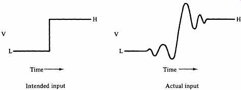
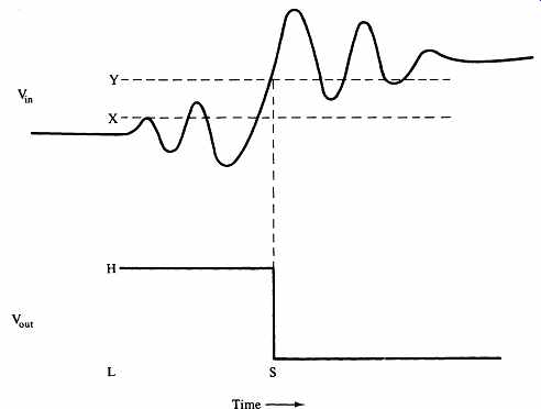
FIG. 8. How the Schmitt trigger removes noise.
Let us put this waveform into a Schmitt trigger and see what happens. In FIG. 8, the sloppy input waveform with the Schmitt trigger switching voltages X and Y is shown. The input must rise to Y before the Schmitt trigger will switch.
The hysteresis in the Schmitt trigger rejects all the noise in the lower part of the signal, and a clean switch occurs in the output at point S. Once switched, the Schmitt trigger will ignore voltage excursions above X. The hysteresis in the Schmitt trigger has cleaned up the terrible waveform and recaptured the original intent.
Schmitt triggers have another important application with slowly varying input voltages. A standard low-power Schottky gate interprets H as being > 2.0 V and an L as < 0.8 V. Voltages in the forbidden region between 0.8 V and 2.0 V can cause indeterminate or even oscillating outputs. The outputs of normal gates switch through the forbidden region so fast that subsequent inputs are not confused. Problems can arise if the inputs receive slowly changing signals, such as from a 60-Hz alternating current or a charging or discharging capacitor. To use such signals in logic circuits, you must first feed them into Schmitt triggers, whose "snap" action (hysteresis) produces clean, fast output transitions, no matter how slowly the inputs change.
A POWER-ON RESET CIRCUIT
Orderly startup of a digital system requires that certain crucial flip-flops be set to known values when power is applied. We need a reset signal that will come on for a short time as the power supply is coming up to voltage, and will then go off and remain off.
A resistor-capacitor combination provides a slowly increasing voltage across the capacitor in response to a step (rapidly increasing) input voltage. We made use of this property in the single-shot delay circuit discussed in Section 4. If we feed this slowly increasing voltage into a Schmitt trigger, we have a circuit that produces an immediate H signal as output, and then switches to L as the capacitor charges during power up. FIG. 9 shows the circuit and the waveforms resulting from the power-up sequence. The duration of the reset signal is roughly the product of Rand C: t = R x C, where R is in ohms, C is farads, and tin seconds.
NEXT>>
Related Articles -- Top of Page -- Home