AMAZON multi-meters discounts AMAZON oscilloscope discounts
This SECTION offers an overview of the basic types of sensors used to detect optical and near-infrared radiation.
1. Photosensors
Detection of light is a basic need for everything from devices to plants and animals. In the case of animals, light detection systems are very highly specialized, and of ten operate very near to thermodynamic limits to detection. Device researchers have worked on techniques for light detection for many years, and have developed devices that offer excellent performance as well.
Clearly, the military has been a major sponsor of light detection device research.
Devices for light detection are of fundamental importance throughout military technology, and the maturity and widespread availability of inexpensive photosensors is a direct result of this DOD research investment over many years.
Light is a quantum-mechanical phenomena. It comes in discrete particles called photons.
Photons have a wavelength ?, a velocity c m s = × 3 10^8 , a frequency ohm p
2 c , energy E hc h Js = = × -
? where 6 67 10 34
. , and even a momentum P h
Among all of this, it is important to remember the relationship between energy and wavelength. In all cases, the energy of the photon determines how we detect it.
Light detectors may be broken into two basic categories. The so-called quantum detectors all convert incoming radiation directly into an electron in a semiconductor device, and process the resulting current with electronic circuitry. The thermal detectors simply absorb the energy and operate by measuring the change in temperature with a thermometer.
Quantum Detectors
We will start by examining the quantum detectors, since they offer the best performance for detection of optical radiation.
In all of the quantum detectors, the photon is absorbed and an electron is liberated in the structure with the energy of the photon. This process is very complicated, and we will not examine it in detail. It is important to recognize that semiconductors feature the basic property that electrons are allowed to exist only at certain energy levels. If the device being used to detect the radiation does not allow electrons with the energy of the incident photon, the photon will not be absorbed, and there will be no signal.
On the other hand, if the photon carries an amount of energy which is "allowed" for an electron in the semiconductor, it can be absorbed. Once it is absorbed, the electron moves freely within the device, subject to electric fields (due to applied voltages) and other effects. Many such devices have a complicated "band structure" in which the allowed energies in the structure change with location in the device. One example of such a "band structure" is that offered by a p-n diode. In a diode, the p-n junction produces a step in the allowed energy levels, resulting in a direction in which currents flow easily and the opposite direction in which current flow is greatly reduced.
A photodiode is simply a diode, biased against its easy flow direction ("reverse-biased") so that the current is very low. If a photon is absorbed and an electron is freed, it may pass over the energy barrier if it possesses enough energy. In this respect, the photodiode only produces a current if the absorbed photon has more energy than that needed to traverse the p-n junction. Because of this effect, the p-n photodiode is said to have a cutoff wavelength-photons with wavelength less than the cutoff produce current and are detected, while photons with wavelength greater than the cutoff do not produce current and are not detected.
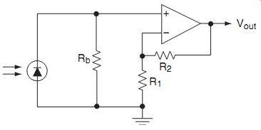
FIG. 1.1: Connection of a photodiode in a photovoltaic mode.
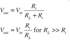
Photodiodes may be biased and operated in two basic modes: photovoltaic and photoconductive. In the photovoltaic mode, the diode is attached to a virtual ground preamplifier as shown in FIG. 1.1, and the arrival of photons causes the generation of a voltage which is amplified by the op-amp. The primary feature of this approach is that there is no dc-bias across the diode, and so there is no basic leakage current across the diode aside from thermally generated currents. This configuration does suffer from slower response because the charge generated must charge the capacitance of the diode, causing an R-C delay.
In the photoconductive mode, the diode is biased, and the current flowing across the diode is converted to a voltage (by a resistor), and amplified. A photoconductive circuit is shown in FIG. 1.2. The primary advantage of this approach is that the applied bias decreases the effective capacitance of the diode (by widening the depletion region), and allows for faster response. Unfortunately, the dc bias also causes some leakage current, so detection of very small signals is compromised.
In addition to making optical detectors from diodes, it is also possible to construct them from transistors.
In this case, the "photocurrent" is deposited in the base of a bipolar junction transistor. When subjected to a collector-emitter bias (for npn), the current generated by the photons flows from the base to the emitter, and a larger current is caused to flow from the collector to the emitter. For an average transistor, the collector-emitter current is between 10 and 100× larger than the photocurrent, so the phototransistor is fundamentally more sensitive than the diode.
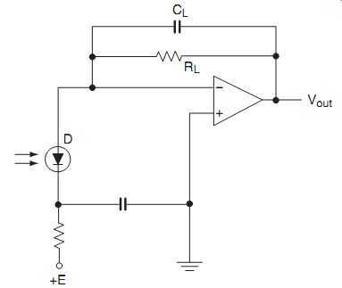
FIG. 1.2: Photoconductive operating mode.
Photodiodes and phototransistors are very widely available. Most semiconductor device manufacturers also offer photodiodes and transistors, so there are nearly 100 suppliers.
More than 10 manufacturers specialize in photosensors. As a result, optimized photodiodes and transistors are available at very low cost.
These devices are also available in packages designed for particular applications.
For example, it is common to use a light-emitting diode and a detector mounted in a pair so that passing objects can interrupt the optical beam between them. Opto-interruptors consisting of such emitter-detector pairs are available in a wide variety of configurations. Proximity detectors situated side by side sense the presence of a reflecting surface by causing reflected light to strike the detector.
Other applications of optical detector-emitter pairs include measurement of the rotation rate of electric motors. In this case, a disk is mounted on the shaft of the motor with a large number of slits cut through it. The detector emitter pair is mounted so that the slits cause an oscillation in the signal-and the rotary position can be determined by counting the peaks in the signal. This is called an optical encoder, or an incremental encoder, and it is widely used in electric motors, as shown in FIG. 1.3.
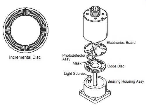
FIG. 1.3: Incremental encoders.
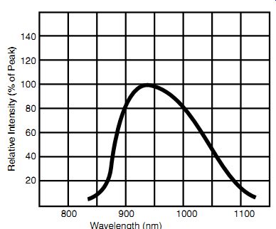
FIG. 1.4: Typical photodiode spectral response.
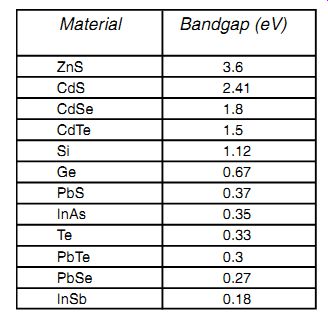
Table 1.1: Bandgaps of some semiconductors.
Most phototransistors and photodiodes have their peak sensitivity in the near infrared (see FIG. 1.4). The peak sensitivity occurs near the cutoff wavelength (near 1 µm) and extends to shorter wavelengths. The location of this peak sensitivity is due to the energy of the "bandgap" in silicon, and is not easily adjusted.
Photosensors can be made from other electronic materials with different bandgaps, as shown in TABLE 1.1. None of these materials are as widely available as silicon, and costs for detectors made from InSb can be substantially higher.
There is another important consideration to keep in mind when selecting photosensors. In addition to the photocarriers in the device, thermally generated carriers can be produced. The distribution of energies generated by thermal processes is dependent on the thermodynamics of the device, and on the temperature. Because of this relationship, increasing the temperature causes an increase in the number of thermally generated carriers. Conversely, reducing the bandgap of a room-temperature device will also cause an increase in the number of thermally generated carriers. Silicon detectors work well at room temperature, but heating to more than 100°C starts to cause substantial increases in "dark current." Detectors made from materials other than silicon may offer increased cutoff wavelength, but may also require cooling below room temperature.
In general, there is a nearly linear relationship between the maximum operating temperature and the cutoff energy for the detector. By selecting a material with a cutoff energy one-fifth that of silicon (such as InSb), it is necessary to cool the device to about one-fifth of the maximum operating temperature of silicon (cooling to 77K is optimal for InSb). This tradeoff between cutoff and operating temperature imposes severe cost issues for operation of devices at fairly long wavelengths.
If cooling is affordable, a large selection of materials and devices with "engineered band-gaps" is available. The tremendous interest in devices with cutoff wavelengths near 10-20 µm is a direct result of the DOD interest in infrared detectors for night vision. It turns out that the peak of the infrared spectrum for objects at room tempera ture is in this region, and so the maximum contrast in thermal detection is available by producing devices with sensitivity in this region.
There is a simple relationship between the temperature of an infrared source and the peak wavelength of the blackbody spectrum.
?m T
=
2898
where the wavelength is in microns, and the temperature is in Kelvin. So, for room temperature, the maximum wavelength is near 10 microns.
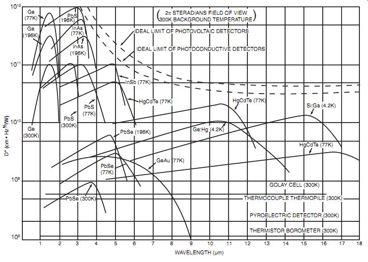
FIG. 1.5: Typical spectral response of IR detectors.
Of the materials most studied, the clear winner is Mercury Cadmium Telluride (MCT). It may be formulated to have cutoff between 10 and 20 microns, and offers excellent properties for infrared detection. In particular, it offers low dark current, high absorptivity, and low carrier scattering. Unfortunately, it is difficult and ex pensive to manufacture. As should be expected for anything containing mercury, its fabrication process is an environmental nightmare, and the basic material is not compatible with electronics. As a result, it is "bump-bonded" onto silicon substrates for readout and signal processing. In addition, it must be operated at or below 77K, which imposes operational complications. A commercial imaging system based on MCT detector arrays generally costs near $100,000 at the present time.
Most military applications (ballistic missiles, aircraft imaging systems, satellite systems) can afford this set of costs and complications, but commercial and civilian applications are generally cost-constrained. Therefore, recent research activities have focused on other materials which might be less expensive to make and operate.
InSb does not offer sensitivity in the 10-20 µm region, but is more easily made than MCT, is electronics compatible, and can be operated near 100K. Research to extend the operation to higher temperatures is underway throughout academia and industry.
Overall, the relationship between cutoff and operating temperature is fairly strict.
MCT, which has been the focus of billions of dollars of materials research effort, has only been slightly extended to higher temperatures. There is not tremendous hope that InSb or other materials will benefit from a large change in operating requirements.
The other type of optical detector, the thermal detector, does offer some hope for this problem.
Thermal Detectors
Thermal detectors operate by absorbing the infrared radiation and measuring the temperature rise of the detector with a thermometer. Generally, the performance of thermal detectors is limited by the availability of sensitive and small heat capacity thermometers.
An important advantage of thermal infrared detectors is due to the absence of any relationship between the wavelength of the absorbed radiation and the response of the detector. Any energy absorbed causes a response in the detector. Therefore, it is possible to use a thermal infrared detector at room temperature to detect radiation from room temperature blackbodies. However, it is important to note that if the conditions allow use of a quantum detector, such a detector will outperform a thermal detector by several orders of magnitude. Thermal detectors come into their own in situations that don't allow quantum detectors.
Since the thermometer is mounted within the infrared detector structure, it is connected to a temperature reference by a finite thermal conductance. This finite conductance imposes dynamic constraints on the system behavior, and we may analyze the situation as follows:
Assume we have a thermometer that is a thermistor with a temperature coefficient given by:
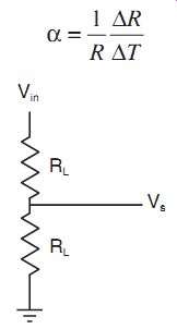
FIG. 1.6: Voltage divider.
This thermistor is mounted in an electrical circuit with a load resistor with a resistance of RL, and is biased by a dc voltage of Vin. The electrical circuit is shown in FIG. 1.6.
As in all voltage dividers, we have:
The sensitivity of this system is given by:
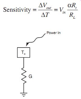
FIG. 1.7: Thermal circuit.
However, we must consider the thermal characteristics of this system as well. In this case, we model the thermometer as a finite heat capacity attached to an object by a finite thermal conductance. Infrared power is deposited into the thermometer, causing the temperature of the thermometer to oscillate. This thermal situation can be modeled as a thermal circuit as shown in FIG. 1.7.
By energy balance, the energy gained is equal to the change in energy of the thermometer:

To improve the sensitivity, it is important to choose a thermometer with a large temperature coefficient and a small heat capacity. We can see from this expression that the response of the detector will have a simple 1-pole response, which is to say that it is frequency-independent below the cutoff frequency and decreases as 1/f above the cutoff. Its response is exactly the same as that of an electrical low-pass filter.
There are several different infrared detectors based on this detection concept. In fact, almost every well-established thermometer has also been optimized as an infrared detector.
Phototransistor Example
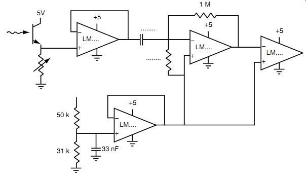
FIG. 1.8: Phototransistor circuit.
The phototransistor is a device that operates by converting incoming photons to electrons in the base of a bipolar transistor. As for any such transistor, the base current causes a larger collector-emitter current to flow, which is detected by a circuit. The easiest way to detect a current is to use a resistor to convert it to a voltage, as shown in FIG. 1.8.
In this case, an oscillator circuit is powering a light-emitting diode, causing a light oscillation at 1 kHz. The phototransistor is pointed at the LED, and detects the oscillation in the incident light. The circuit converts the current to a voltage with a pull-down resistor, buffers the signal, high-pass filters the signal, and then converts it to a square wave with a comparator. This circuit is one of many possible such circuits, and may be considered typical.
We can see that the signal at the beginning of the circuit reflects the oscillation as well as the background illumination (dc and 60-Hz components). Some of the filter design is intended to reduce the sensitivity to these "noise" components while preserving the sensitivity to the signal at 1 kHz.
The variable resistor at the front of the circuit is an important degree of freedom. The current flowing through the transistor cannot exceed the saturation current:

…where Vbias is the total collector-emitter voltage, and Rpd is the value of the pull-down resistor. If the background is very bright, the current flowing in the device may already be very close to the saturation value, and any additional signal illumination will not produce much additional signal.
Depending on the amount of background illumination, it is possible to saturate the detector, thereby reducing the sensitivity to signals. We use a variable resistor here to allow adjustment so that the detector is biased at a point of good performance.
It is possible to obtain such detectors in side-by-side emitter-detector pairs, which cause a signal only if a reflective object is nearby. Depending on the biasing and the background illumination, it is possible to detect objects at a range of more than 1 cm.
2. Thermal Infrared Detectors
In recent years, the Department of Defense (DOD) has invested a great deal of research and development funds into detection techniques that allow long-wave detection from uncooled platforms. An additional focus of this work has been techniques that are compatible with the formation of dense arrays. One interesting device that has emerged due to this investment has been the Uncooled Detector arrays made by Honeywell.
These detectors are based on the simplest thermal design-a resistance thermometer.
What is novel about this device is that it combines the best microfabrication technology with good thermometer technology and electronics integration.
A drawing of the microbolometer is shown in FIG. 2.1. The basic idea is to use silicon microfabrication techniques (such as those in many accelerometers) to make an isolated thermal structure with very little heat capacity. As we saw in the thermometer discussion, the thermal infrared detector is improved by minimizing the heat capacity.
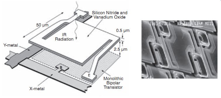
FIG. 2.1: Microbolometer.
In the final device, a flake of silicon nitride with dimensions of 50 µm × 50 µm × 0.5 µm is floated above a silicon substrate. This flake is supported by a pair of legs, and is coated with a resistive material with a good thermal coefficient of resistance. Underneath the flake is a transistor that is used to connect the current-measuring circuit to the device using a conventional row-column addressing technique. The device cur rent is passed out to a processing circuit on the perimeter of the device by the x and y metal leads.
In this device, much research went into developing a technique for depositing the nitride on top of a transistor, for releasing the devices with very high yield, and for obtaining a sensitive thermometer in the form of a deposited metal film. This resistor is made from vanadium oxide, which offers a TCR of about 1% near room tempera ture. The resistance change is a result of a structural phase transition in vanadium oxide above room temperature, so this device must be held near room temperature to allow operation with good sensitivity.
Having developed this technology, Honeywell has gone on to make dense arrays (200 × 200), and to continue optimizing the performance of the devices. In the last couple of years, a complete camera system has been demonstrated. This base technology has been offered for licensing, and is presently being commercialized by several manufacturers of infrared imaging systems.
This device does not out-perform the MCT imager, but it does enable operation at room temperature, and might be available at low cost with further development.
Typical Teflon lenses used in motion detection systems are made with a surface texture that includes several circular bumps. These bumps act as focusing lenses, and will bring light from a particular part of the scene to the detector. As a warm object moves through the scene, radiation is occasionally focused on the detector, causing a transient in signal that is detected.
A typical motion detector allows the setting of a threshold, which is simply an electrical threshold in the detection circuit, and an output voltage which indicates the threshold has been crossed recently. Usually, you can also set the duration of illumination after a detection event.
Many such products are now available on the market at very low prices. There has been a recent substantial improvement in the availability of low-quality, inexpensive IR sensors, and a family of devices adequate for imaging systems are emerging.
NEXT: Position and Motion Sensors
PREV: