In recent years the use of large amounts of negative feedback in audio amplifiers has become controversial. Several people have examined the time-response properties of feedback amplifiers and have concluded that amplifiers which employ large amounts of negative feedback are prone to a form of high-frequency distortion called "transient intermodulation distortion" (TIM) [1-4]. Simply put, this distortion is said to occur when a signal changes too quickly for the amplifier to follow it properly.
The observation that a large amount of negative feedback causes TIM tends to run counter to the conventional wisdom that increased negative feedback generally improves a given amplifier's performance, so long as adequate stability is preserved. Several other researchers have recently questioned these findings and conclude that large amounts of negative feedback do not increase the possibility of TIM and can in fact improve amplifier performance as long as the amplifier has an adequate slew rate [5,6]. TIM is thus a popular subject surrounded by a certain amount of controversy. It has also become a frequently cited reason for degraded sound. Advertisements indicate that several manufacturers have been influenced by the discussions as well, some proudly pointing out that they use very little negative feedback.
Much of the misunderstanding and disagreement surrounding the subject seems to stem from inadequate consideration of the trade-offs and constraints involved in the application of negative feedback, especially as it relates to contemporary, real-world amplifier circuits. This is particularly true of feedback compensation. For this reason, we will take the time to review important negative feedback principles where necessary. Given a good understanding of negative feedback as it is applied to audio amplifiers, some of the TIM issues should become easier to resolve.
Before proceeding, we should point out that TIM, which is associated with negative feedback and its compensation, is only one form of high-frequency intermodulation distortion.
The term "dynamic intermodulation distortion" (DIM) has been used to describe the general class of intermodulation distortions which depend on frequency as well as amplitude.. TIM is thus one form of DIM. Since the product of frequency and amplitude implies rate-of-change, and since the maximum rate-of-change that an amplifier can follow is called its slew rate, the term "slew induced distortion" (SID) has also been used as a label for DIM. These distinctions are, however, relatively weak and unimportant, referring more to the mechanism than to the measured or audible effect. Because it is the source of most of the controversy, we will concentrate on TIM; however, our discussion will consider other sources of DIM as well, some of which may in practice be more serious.

Fig. 1-Post-RIAA spectral distribution for phonograph records.
Transient Intermodulation Distortion
First, let's take a look at the popular TIM arguments to get some background. What follows is a sort of composite paraphrasing of many of the arguments which have appeared.
Feedback amplifiers operate on the principle that a large portion of the input signal is cancelled by feedback from the amplifier output, leaving a small signal-plus-error which
drives the amplifier so as to produce the desired output. In amplifiers with large amounts of negative feedback, this signal-plus-error is forced to be very small and thus, in theory, low distortion results. Under these conditions, the net gain with feedback (closed-loop gain) depends almost exclusively on how much of the output signal is fed back; i.e., if one tenth of it is fed back, the gain will be 10. The large feedback factor (ratio of gain without feedback to gain with feedback)
is obtained by putting a large amount of gain in the forward path or open-loop amplifier. The open-loop amplifier is thus very sensitive and will overload if the error, for some reason, gets at all appreciable.
All amplifiers have a finite delay from input to output. If a feedback amplifier is driven with a signal having a very fast rise time (like the leading edge of a square wave), there will be a brief interval during which the open-loop amplifier sees the full input signal, undiminished by negative feedback which hasn't yet gotten back to the input. Overload will thus occur and distortion will result. The more sensitive inputs of amplifiers with high feedback factors are that much more prone to such an overload.
Since this form of distortion is brought about by fast transients in the input signal and because an overload condition causes intermodulation distortion, the phenomenon is referred to as transient intermodulation distortion (TIM). Returning to the origins of TIM, the situation is further aggravated by the additional slowness of response introduced in the open-loop amplifier by necessary feedback compensation. Each stage in a multi-stage amplifier introduces phase shift that increases with frequency. Feedback compensation rolls off the open-loop response so that the feedback factor falls below unity before enough excess phase shift accumulates to cause instability or peaking in the closed-loop response. The frequency where the feedback factor falls to unity is called the gain crossover frequency. In order to achieve a stable gain crossover frequency, the 6 dB/ octave compensation roll-off must begin at some lower frequency. Amplifiers with large feedback factors (at low frequencies) have more gain to "get rid of" and must start their compensation roll-off at a lower frequency, resulting in a smaller open-loop bandwidth. An amplifier with 20 dB of feedback needn't start its roll-off until 100 kHz for a 1-MHz gain crossover, while one with 60 dB of feedback must start at 1 kHz. The latter amplifier, with heavier feedback compensation and a long open-loop time constant, is thus slower in responding to input signals.
In responding to a fast input signal (e.g., a square wave), a large internal voltage or current overshoot will be produced in order to quickly charge the compensating capacitor and overcome the effect of the long time constant it introduces.
The large overshoot is produced during the interval between the fast input change and the time when the feedback catches up with the input, when a large difference or error signal is applied to the open-loop amplifier.
In some cases this overshoot may be 10 to 100 times as large as the nominal signal levels at that point. Unfortunately, the stages prior to the compensation point cannot always handle such a large signal without nonlinearity or outright clipping. If the overshoot causes these stages to clip or generate distortion, TIM results. When these overshoots are clipped, the amplifier is into the well-known phenomenon of slew-rate limiting.
It can be shown mathematically that if the input signal is bandlimited to a frequency less than the open-loop bandwidth of the amplifier, no overshoot can occur, even if the input signal is a bandlimited square wave. Thus, wide open-loop bandwidth eliminates the possibility of TIM caused by overshoots. Having wide open-loop bandwidth, in turn, places a limit on the feedback factor for a given gain crossover frequency. For example, if we choose an open-loop bandwidth of 20 kHz and a gain crossover frequency of 1 MHz, then we are limited to a feedback factor of only 34 dB. The above explanation of TIM seems plausible enough, and it has appeared in various forms in many places. It is the origin of the popular belief that small feedback factors and wide open-loop bandwidth are necessary for minimizing TIM. Although it may at first glance seem convincing, this explanation is somewhat oversimplified and misleading.
While some of the issues have been analyzed in great detail in technical papers, other more important considerations have been ignored. In several respects, the problem seems to lie with not seeing the forest for the trees. A few more recent papers have, however, done a very good job in lending insight and perspective to some of the more important issues [5,6]. The approach taken here will involve less detail and more scope and perspective. For example, we'll attempt to determine just how fast audio program signals really are. The length of the unavoidable time delay in the amplifier and how it is affected by feedback compensation is another important area in need of discussion. We will also examine the conditions governing overload of an amplifier's internal stages. This will be done in the context of a practical amplifier topology with realistic combinations of feedback factor and open-loop bandwidth. Recognizing that in addition to limits on amplitude, amplifiers are limited to providing a maximum rate-of-change at their output, much attention will be paid to amplifier slew-rate performance and its relationship to TIM. Finally, techniques for measuring amplifier TIM performance will be discussed.
Program Characteristics
Just as all real amplifiers are bandlimited, so are all real program sources. No program source will ever produce a square wave with razor-sharp edges. In fact, not only are program sources bandlimited in the small-signal sense, but they are more seriously limited in large-signal bandwidth, or power bandwidth. As an example, a fine tape machine might be flat to 20 kHz at low levels, but it typically cannot produce anywhere near full output at 20 kHz. Such restrictions are usually due to equalization which pre-emphasizes the high frequencies so that the subsequent de-emphasis at the reproducing end will reduce high-frequency noise. High frequencies will, therefore, overload the medium more readily than low frequencies. Such equalization characteristics are common to almost every type of program source, including phonograph, FM, and tape. As a result, the maximum high-frequency output of each program source is constrained to rather well-defined limits.
Since signals with a large rate-of-change or "time derivative" are generally the cause of TIM, we need a way of characterizing the tendency of a given program source to produce them. Such a measure should not be absolute, like time derivative, but rather should be relative so that it can be applied equally well at different points in the system regardless of signal level. We will therefore use the ratio of peak time derivative to peak amplitude expressed in "volts-per microsecond per volt" (V/ Ns)/V, and call it the normalized time derivative. The inverse of this quantity is similar to, but not quite the same as large-signal rise time. Knowing the normalized time derivative, we can go to any point in the system and, given the maximum amplitude at that point, determine the commensurate maximum time derivative.
With the exception of a microphone, the best source of fast program signals in the home is probably the phonograph. However, its performance is well-constrained by mechanical processes such as tracking. The performance is also well characterized. In Fig. 1, the dots are a scatter plot of maximum observed output levels at various frequencies from a survey of many records. These data were taken from the familiar trackability diagram widely published by Shure Bros. [7]. While the usual presentation is in terms of groove velocity, this information has been RIAA equalized and normalized to 25 cm/S at 1 kHz and 1 V peak. It shows what actually can be expected at the output of one's phono preamp (as shown, the data are not useful for points in the system prior to RIAA equalization, such as the phono preamp input). The data represented by the X's are spectral data for a single cymbal crash and were presented by Tomlinson Holman [8]. The crash is one from a Sheffield Lab direct-to-disc recording which is noted for its tracking difficulty.
With reference to Fig. 1, we see that the highest amplitude occurs at 4 kHz and is 1.35 V peak, while the highest time derivative occurs at 10 kHz and is 0.035 V/ pS. This results in a normalized time derivative of only 0.026 (V/ pS)/V. Thus, in a system subjected to a wide variety of material such as represented by the dots of Fig. 1, a point in the system which must handle an amplitude of 1 V peak with low distortion must handle a time derivative of 0.026 V/ pS with equally low distortion.
Before proceeding further, we should take note of the fact that an advanced treble control will tend to increase the normalized time derivative of the program, but not as much as one might at first think. The reason for this is found upon further examination of Fig. 1. The peak time derivative will increase in proportion to the greater amplitude of the high frequency signals. However, most treble control action occurs between 2 kHz and 10 kHz, meaning that the overall peak amplitude (occurring at 4 to 5 kHz in Fig. 1) will increase somewhat as well. Based on these observations, we can conclude that 6 dB of treble boost will increase the normalized time derivative by perhaps 50 percent.
While the cymbal crash exhibits substantial ultrasonic content, its amplitude generally lies below the envelope of the other points. Notice that its mid-band recording level is actually rather low in comparison. Taken alone, the normalized time derivative for the cymbal crash might be fairly high, but the ratio of interest must be based upon the peak amplitude for all the music.
Even if the three highest points on Fig. 1 are ignored, an overall power bandwidth of less than 10 kHz is obtained, and a maximum normalized time derivative of approximately 0.05 (V/ p S) /V results. By comparison, a 20-kHz sinusoid has a normalized time derivative of 0.126 (V/ p S) /V. Music, of course, produces many simultaneous points whose amplitudes and time derivatives add in some fashion to produce a total amplitude and a total time derivative for the complete spectrum. We can gain further insight by recognizing that for mid-band frequencies between about 500 Hz and 2 kHz, post-RIAA amplitude is directly related to recorded velocity. Above 2 kHz, post-RIAA time derivative and recorded velocity are directly related, i.e., a 50-cm/S, 10-kHz component produces the same time derivative at the output of the phono preamp as a 50-cm/S, 20-kHz component. This latter relationship is due to the integrating effect of the 2-kHz RIAA high-frequency roll-off. Knowing this, we can get a good idea of the normalized time derivative by assuming realistic values for the maximum total mid-band velocity and the maximum total high-frequency velocity. Notice that a smaller assumption for the maximum mid-band velocity yields a larger normalized time derivative. Keep in mind that the mid-band and high-frequency maxima need not occur simultaneously.
As an example, if we assume a maximum mid-band velocity of 25 cm/S and a large maximum high-frequency velocity of 150 cm/S (probably impossible to track), we arrive at a figure of 0.076 (V/pS)/V. Based on this figure, a 100-watt amplifier which can deliver 40 V peak with an 8-ohm load must cleanly reproduce signals with 3 V/ p S time derivatives.

Fig. 2-Compensated and uncompensated power amplifier open-loop gain vs. frequency.
This figure may seem very small to some people, but the term "cleanly" is the key here. We are certainly not talking about the ultimate slew-rate capability of the amplifier, which generally occurs under nonlinear operating conditions. Clearly the amplifier must have some operating margin in order to satisfy the "cleanly" requirement. As we shall see later, in some cases this required slewing margin can be substantial.
Although it is very unlikely that any material will approach the 0.076 (V/ p S) /V, figure, we can be even more conservative if we wish and simply say that a full-amplitude 20-kHz sinusoid, 0.125 (V/pS) /V, must be handled with adequate slewing margin. Requiring that a square wave bandlimited to 20 kHz, 0.25 (V/ p S) /V, be handled cleanly would add yet another factor of two in conservatism.
Based on these observations, we may conclude that real audio signals are not nearly as fast as some would like to believe. However, this is not cause for complacency with respect to TIM: It merely gives us a more realistic perspective for dealing with the problem.
Low-Pass Filtering
It has often been suggested that a low-pass filter (LPF) be placed ahead of the power amplifier to assure that the program bandwidth does not exceed the open-loop bandwidth of the amplifier in order to minimize TIM [1-3]. Although we will see later that such a precaution has no bearing on TIM susceptibility, it is worth noting that the LPF will place a limit on the power bandwidth, and thus the time derivative, of signals applied to the power amplifier. In this latter respect, the LPF could prevent TIM if such a limitation were necessary. However, our earlier discussions showed 'that the power bandwidth of real audio signals is considerably less than 20 kHz. Assuming that an LPF cutoff of less than 40 kHz is unacceptable due to frequency-response error (-1 dB at 20 kHz assuming first-order cutoff), it is quite safe to say that such a filter will have no effect on TIM produced by program signals.
Ticks, pops, and mistracking may, however, produce considerably larger normalized time derivatives than program, at least in the case where wideband moving-coil cartridges are employed. Values as high as 0.1 to 0.2 (V/ p 5) /V may be encountered. However, even a step input will only be limited to 0.25 (V/ p S) /V by a 40-kHz LPF. The filter will thus have only a limited effect on the smaller normalized time derivative of the ticks, pops, and mistracking. One also has to wonder how important TIM-free reproduction of these annoying signals really is. It is probably sufficient that slew-rate limiting not be encountered in the system under these conditions.
The only sensible reason for an LPF seems to be improved immunity to r.f. interference, if this is required.
Feedback Compensation
As mentioned earlier, feedback operates on the principle of feeding a portion of the output back to the input for comparison with the input signal. The loop so formed may be unstable if the phase of the signal is incorrect. Feedback compensation is employed to assure stability by controlling the net gain and phase shift a signal sees as it goes around the complete loop.
Since the role played by feedback compensation is crucial to the TIM distortion mechanism, and since in many TIM discussions it is not adequately considered, it is appropriate at this point to take a look at feedback compensation.
Because all real amplifiers have finite bandwidth, the gain and thus the feedback factor must begin to roll off at some frequency. In a multi-stage amplifier, each stage usually contributes one or more "poles" (6 dB/octave roll-offs) and accompanying phase shift. If at some high frequency we have too much phase shift while we still have gain around the loop, we will have positive feedback and thus an oscillator.
For this reason, the frequency at which the feedback factor has decreased to unity (i.e., the gain crossover frequency) is very important in determining amplifier stability. To prevent oscillation, the phase shift accumulated beyond the fixed 180-degree loop inversion must be less than 180 degrees at this frequency. In general, good engineering practice requires that less than about 135 degrees be accumulated, leaving a phase margin of at least 45 degrees. In order to obtain the required stability, feedback compensation is employed to deliberately roll off the gain so that the feedback factor goes below unity before too much phase shift accumulates.
The open-loop gain as a function of frequency for a typical power amplifier before and after feedback compensation is shown in Fig. 2. The closed-loop gain is shown as a dotted line at 26 dB, and the feedback factor is simply the distance between the solid and dotted curves. It is important to remember that each roll-off contributes phase shift (phase lag or delay) which increases with frequency, but which can never exceed 90 degrees. At its 3-dB point, or "corner frequency," each roll-off generates 45 degrees. The gain and phase characteristics for a single pole are shown in Fig. 3. Notice that a single pole placed at a low frequency can create a great deal of high-frequency loss without ever introducing more than 90 degrees of phase shift. This is the basis for what is called lag compensation.
A design with many poles situated below the gain crossover frequency will tend to be unstable, while one with only a single pole below this frequency will tend to be stable, even if that pole is at a very low frequency. The uncompensated amplifier in Fig. 2 crosses over at 2.4 MHz and has three poles below that frequency, while the compensated version crosses over at 1 MHz and has only one pole below the gain crossover frequency. As is the case in Fig. 2, the compensation network usually decreases substantially the frequency of one existing pole and may also significantly increase the frequency of another one. This effect is called pole splitting, and its double benefit further contributes to stability.
To summarize, the objective of feedback compensation is quite simple: Establish a gain crossover frequency low enough to achieve an acceptable phase margin. In a power amplifier, much of the phase shift at high frequencies is contributed by the output transistors, which typically have ft's (current gain-bandwidth products) of about 1 to 4 MHz.
Output stages will tend to contribute rapidly increasing phase shift above this frequency. As a result, reasonable gain crossover frequencies for power amplifiers are generally in the range of 0.5 to 2MHz.

Fig. 3-Gain and phase characteristics for a 1-kHz pole.
A Typical Power Amplifier To further put things into perspective, we'll now take a brief look at the operation of a practical power amplifier. This simple amplifier will provide a setting for the examples illustrating TIM considerations in the later sections. A simplified version of a popular amplifier topology is shown in Fig. 4.
Transistors Q1 and Q2 form a differential amplifier which is the first stage of the open-loop amplifier. Here the feedback signal applied to the base of Q2 is subtracted from the input signal applied to the base of Q1. Notice that the feedback signal is divided down by R4 and R3, which set the closed loop gain at about 20. Capacitor C2 allows full feedback at d.c. to assure a small output offset voltage.
The voltage difference between the bases of Q1 and Q2 is translated to a current signal which in turn drives the base circuit of the pre-driver, Q3. The resulting voltage signal at the collector of Q3 is delivered to the output with approximately unity gain by the complementary Darlington emitter-follower output' stage. The primary purpose of the output stage is to provide current gain and thus present a relatively high impedance load to the collector circuit of Q3. The collector current for Q3 is provided by a current source so that the only real load at Q3's collector is that presented by the output stage. This arrangement provides very high gain in the pre-driver stage, especially if the current gain in the output stage is high.
The uncompensated loop gain of this amplifier is shown in the top curve of Fig. 2 (assuming transistor betas of 50). Feedback compensation of this amplifier is provided by a single capacitor C3 connected from collector to the base of Q3. This type of compensation is often referred to as Miller-effect compensation.
At low frequencies, C3 is an open circuit and the gain is quite high. At higher frequencies, C3's reactance decreases, and it begins to form a tight negative feedback loop around Q3. At high frequencies, almost all of the signal current from Q1 flows through C3, rather than R2 and the base of Q3.
Under these conditions, we can almost think of Q3 as an operational amplifier and its base node as a virtual ground.
At mid to high frequencies, the voltage at the collector of Q3 is then approximately the signal current from Q1 times the reactance of C3. Furthermore, the open-loop gain of the amplifier will simply be the trans-conductance (gm) of the differential amplifier (here about 10 mA per volt) times the reactance of C3. Since this reactance is decreasing with frequency at 6 dB/octave, so will the open-loop gain of the amplifier. When this gain decreases to 20 we are at the gain crossover frequency (f,), since the feedback path establishes a closed-loop gain (G) of 20. The choice of 84 pF for C3 yields a reactance of about 2000 ohms at 1 MHz, thus setting the gain crossover at that frequency and yielding the lower curve for open-loop gain in Fig. 2. Expressed in general terms,
C3=gm/2πfxGc (eqn. 1)
Notice that low-frequency considerations, such as feedback factor, do not influence the choice of C3.
Propagation Delay
Some authors have reasoned that an amplifier presented with a very fast transient will be without negative feedback for a short period of time until the feedback signal, having suffered inevitable delay, arrives to cancel most of the input signal [1,3]. During this delay time, it is reasoned, some stages in the open-loop amplifier may clip due to the unusually large input signal.

Fig. 4-Simplified schematic of a popular power amplifier design.
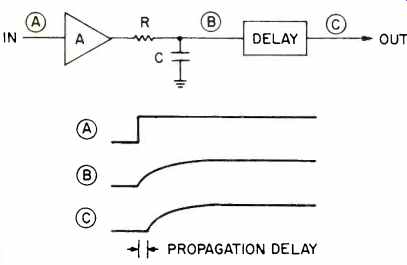
Fig. 5-A simple model of the open-loop amplifier showing time response to
a step input. In practice, gain and delay are distributed throughout the amplifier.
There is little question that such a problem will occur if a square wave with a 1 nS rise time is applied to an audio amplifier. However, to assess the practical likelihood of such a problem, we must consider the time it takes a real program signal to rise, what the delay time really is (it is not the open loop rise time as some have implied), and the overload mechanism of open-loop amplifier gain stages.
The open-loop amplifier can be modeled as a block of gain, a dominant first-order compensation roll-off, and a pure delay as shown in Fig. 5. Effects of the other non-dominant poles are lumped in with the delay with little loss of accuracy. It is well-known that, following a step change at the input of a first-order RC low-pass filter, the output begins to change immediately, no matter how long the RC time constant; only the rate of change will depend on the time constant. Thus, after a sudden change at the amplifier input, the output will begin to change after the above-mentioned pure delay. This is the propagation delay time of the amplifier and is the delay time during which we must be concerned about overloading the amplifier in order to deal with the issue raised above.
The propagation delay time can be estimated by considering the phase margin of the feedback loop. If an amplifier has a phase margin of 45 degrees at a 1-MHz gain crossover, then the total forward path delay (assuming a flat feedback path) must be 135 degrees, of which about 90 degrees is from the compensation pole and 45 degrees is from the propagation delay. This works out to 125 nS. Most power amplifiers will have considerably less propagation delay than this.
It should be pointed out that it is incorrect to say that the amplifier is without feedback during this interval. The closed-loop amplifier is a linear system so long as the gain, roll-off, and delay elements of the model are linear. It is also a continuous system in spite of the delay, and feedback is present 100 percent of the time as long as no stages are clipped. The feedback is, however, continuously "out of date" by a time equal to the delay. Fortunately, the feedback equations readily take this into account in both the frequency and time domains.
Can a full-amplitude input signal, such as a bandlimited square wave, rise far enough in 125 nS to cause any amplifier stages to become nonlinear or to overload? The integrating action of the compensation will prevent stages beyond the compensation from overloading, typically leaving only the input stage before it to worry about (see Fig. 4). Consider as a worst case a 2-V peak square wave bandlimited to 20 kHz. It will rise about 63 mV in 125 nS, and this is enough to drive some input stages into nonlinearity. This is particularly true of the differential pair without emitter resistors (local feedback often called emitter degeneration), as shown in the design of Fig. 4. With a 63-mV error signal driving it, its small-signal gain is less than half its nominal value. This nonlinearity would result in "soft" TIM under these conditions. However, most high-quality amplifier designs have enough local feedback of one sort or another at the input stage to allow good linearity in handling such an error signal. As we will see momentarily, such feedback is usually also an important ingredient in achieving high slew rate.
Feedback factor and open-loop bandwidth are clearly not relevant here, since designs with different values for these parameters could easily have the same input stage design and propagation delay. The important criterion here is to have an input stage that can handle large input signals, at least under transient conditions.

Fig. 6-A model of the feedback amplifier showing the error time response
to a bandlimited step input for various combinations of feedback factor and
open-loop bandwidth.
Closed-loop bandwidth is held constant, and feedback is varied by changing only A2. Input level is assumed to be zero prior to the step.

Fig. 7-Simplified schematic of an improved power amplifier.
Slew Rate
Real power amplifiers are not only limited in terms of output amplitude; they are also limited with respect to the rate of-change or time derivative of the output. When an amplifier is asked to deliver more than its maximum amplitude, it clips and produces a constant amplitude independent of the input signal. Similarly, if an amplifier is called upon to deliver a greater time derivative than its slew rate, the amplifier will go into slew-rate limiting and produce an output rate-of change independent of the input signal. As with amplitude induced distortion, slew-induced distortion (SID), or (TIM), has a gradual onset. It is non-zero below the slew-rate limit and rises as the slew-rate limit is approached.
Having discussed amplifier behavior during the propagation delay interval following a sudden input change, we must now determine if the amplifier can keep up with the time derivative called for by the input signal without being driven into nonlinearity by internal error signals (i.e., overshoots). This is basically a question of margin against slew-rate limiting, since slewing is the result when the internal overshoots are so big they are clipped. Recall that these overshoots are generally the result of the circuit attempting to quickly charge capacitances, particularly the compensating capacitor.
At this point it is important to emphasize that it is the magnitude of these overshoots which is important, not percentage; many papers in the literature have erred in emphasizing the latter [1, 2]. It should be clear that good margin against slew-rate limiting guarantees that the overshoots will not be large enough to cause nonlinearity and thus TIM. How does feedback factor affect slew rate? By itself, not at all. For example, amplifiers with high feedback factors usually have the extra open-loop gain after the point of compensation. The most common example is the use of a current source collector load on the pre-driver stage, as in Fig. 4. Suppose for the moment that the pre-driver stage has a shunt capacitor at its input (base) for compensation (unlike Fig. 4).
If we double the gain after the compensation by some means, we must double the value of the compensating capacitor to restore the gain crossover frequency to its original value. However, the added gain means that we now need only half the time derivative on the capacitor to achieve the same output time derivative, so the magnitude of the current overshoot charging the larger compensating capacitor is unchanged. The percentage overshoot is approximately doubled, however, because of the smaller final value as a result of the doubled d.c. gain. This is illustrated in Fig. 6. Even though the open-loop roll-off starts one octave lower, the input stage doesn't have to work any harder to achieve a given slew rate.
The situation is the same for amplifiers using Miller-effect compensation as in Fig. 4. Here, even the capacitor value is unchanged as the feedback factor is raised or lowered by varying the load impedance of the predriver (Q3). This is so because the feedback action of C3 controls the high-frequency gain rather than the load resistance. Amplifiers which are deliberately designed with low feedback factors typically achieve this by placing a physical load resistance from the collector of the predriver to ground [9].
If we assume that all of the signal current from the input stage can flow into C3, then the slew rate for the amplifier in Fig. 4 is about (0.5 mA/84 pF) = 6 V/ NS. In practice, it will be somewhat less because of some current flow into R2 and Q3.
An improved amplifier is shown in Fig. 7 and is an example of an amplifier with a very high feedback factor. In addition to using a high-quality current source load for the predriver, triple Darlingtons are utilized in the output stage for extra current gain and hence a lighter load on the predriver collector node. Addition of the pair of dotted predriver load resistors, R15 and R16, will convert it to a low-feedback design with a 20-kHz open-loop bandwidth. The required compensating capacitance remains unchanged.
The open-loop gain for the high and low-feedback versions of Fig. 7 is shown in Fig. 8. The gain crossover frequency for both designs is the same, and the only difference is increased loop gain at frequencies below 20 kHz for the high feedback design. The slew rate for both designs is the same for a step input starting at zero volts. This further illustrates the fact that feedback factor and open-loop bandwidth have no effect on slew rate.
What does affect slew rate is the design of the input stage.
For a given size compensating capacitor, an input stage with a higher output current capability will provide an increased slew rate. However, merely increasing the tail current of a simple differential pair stage, as in Fig. 4, will not work because that will increase the stage gain (transconductance) by the same factor. This would then necessitate a proportionately larger compensating capacitor to restore the gain-crossover frequency, and the slew rate would be back to where it was before. One popular solution is to use emitter degeneration.
For example, we can keep the tail current the same, use emitter degeneration to reduce the gain, and then use a smaller compensating capacitor. This approach is used in Fig. 7, where R2 and R3 reduce the gain by a factor of 10. This permits a dramatic increase in slew rate. Local emitter degeneration is also desirable because it increases the overall linearity of the stage and permits linear operation up to a larger percentage of the ultimate slewing capability.
It is important to realize that the extra gain in most amplifiers with high feedback factors is not achieved by adding more voltage-gain stages, which would tend to increase non linearity and propagation delay. As can be seen from Fig. 7, the only elements which need to be added to achieve very high gain are emitter-followers. These stages are practically delayless and actually tend to improve linearity by isolating driving stages from the input nonlinearities of the next stage.
Nonlinearities resulting from transistor beta dependence on collector voltage (Early effect) and current and junction capacitance dependence on voltage are reduced in this way.
It was mentioned earlier that a 100-watt amplifier would have to cleanly handle time derivatives up to about 3 V/pS for worst-case program material. How much margin against slew-rate limiting is required for clean, low-TIM operation? This depends very much on the particular amplifier design. A good design with plenty of local feedback and a linear open loop response may require a margin of less than 1.5 to 1, while a really poor design with gross open-loop nonlinearity could require as much as 10 to 1. However, even the often criticized 741 operational amplifier, when operated under reasonable conditions, requires less than a margin of 5 to 1.
A margin of 4 to 1 should be more than adequate for power amplifiers of reasonable design to guarantee that TIM produced by internal overshoots will be completely inaudible.
Based on this and the previously discussed program characteristics, the 100-watt amplifier should provide a slew rate of at least 12 V/NS. This also gives us a 50 percent margin against slewing in the presence of a 0.2 (V/ NS)/V full-amplitude pop or tick.

Fig. 8-Open-loop gain comparison of amplifiers with high and low feedback
factors and equal gain crossover frequency. The major difference is the greater
feedback in the audio band for the former case.
Notice that we've paid very little attention to what happens when outright slew-rate limiting occurs; rather, we've outlined the conditions required to stay in a rather linear region of operation where, at most, the nonlinearities are soft. This is mainly because TIM will become audible before slew-rate limiting occurs. However, it is worth noting that recovery from a slewing condition for most contemporary amplifier topologies is not affected by the open-loop time constant. This was not necessarily the case in some very early transistor amplifier designs in which a transistor could saturate during slewing and charge the compensating capacitor to an abnormal voltage. Recovery in modern amplifiers is not significantly longer than the time it takes the output to slew to the new signal value.
At this point, it should be clear that slew rate is the most important single parameter governing TIM performance, while feedback factor and open-loop bandwidth have no bearing on TIM. In Part II, we'll continue by looking at other causes of high-frequency or dynamic intermodulation distortion (DIM), why a large feedback factor is good instead of bad, and techniques available for measuring TIM in the lab.
References
1. Otala, M., "Transient Distortion in Transistorized Audio Power Amplifiers," IEEE Transactions on Audio and Electro-acoustics, Vol. AU-18, pp. 234-239, Sept., 1970.
2. Otala, M., and E. Leinonen, "The Theory of Transient Intermodulation Distortion," IEEE Transactions on Acoustics, Speech and Signal Processing, Vol. ASSP-25, No. 1, pp. 2-8, Feb., 1977.
3. Leach, W. M., "Transient IM Distortion in Power Amplifiers," Audio, pp. 3441, Feb., 1975.
4. Greiner, R. A., "Amp Design and Overload," Audio, pp. 50-62, Nov., 1977.
5. Jung, W. G., M. L. Stephens, and C. C. Todd, "Slewing Induced Distortion and Its Effect on Audio Amplifier Performance-With Correlated Measurement Listening Results," AES Preprint No. 1252 presented at the 57th AES Convention, Los Angeles, May, 1977.
6. Garde, P., "Transient Distortion in Feedback Amplifiers," four. of the Audio Engineering Society, Vol. 26, No. 5, pp. 314-321, May, 1978.
7. Kogen, J., B. Jacobs, and F. Karlov, "Trackability-1973," Audio, pp. 16-22, Aug., 1973.
8. Holman, T., " Dynamic Range Requirements of Phonographic Preamplifiers," Audio, pp. 72-79, July, 1977.
9. Leach, W. M., "Build a Low TIM Amplifier," Audio, pp. 30-46, Feb., 1976.
10. Leinonen, E., M. Otala, and J. Curl, "A Method for Measuring Transient Intermodulation Distortion (TIM)," Jour. of the Audio Engineering Society, Vol. 25, pp. 170-177, April, 1977.
11. Cordell, R. R., "A Fully In-Band Multitone Test for Transient Intermodulation Distortion," AES Preprint No. 1519 presented at the 64th AES Convention, New York, Nov., 1979.
by Robert R. Cordell (adapted from Audio magazine, Feb 1980)
= = = =