by Martin Clifford
THE TRANSITION from tubes to transistors in high-fidelity equipment was not without its anguish, for a number of tubes, particularly those for the output stages of power amplifiers, gave excellent results. Tubes, though, were (and are) afflicted with a number of disadvantages. The indirectly heated cathode system means more watts from the a.c. power line. Further, these extra watts result in heat, the arch-enemy of resistors, capacitors, and other miscellaneous parts used in hi-fi components. Tubes also require a certain amount of warm-up time. And, added to this list of woes, tubes need relatively frequent replacement if a high-fidelity system is to be maintained at peak performance.
Solid-state devices, so-called because electrons move through a solid material rather than the vacuum of the tubes, form a rather large family of which transistors are just one member.
Transistors require no warm-up time, have a longer life than tubes, take up less room, do not need sockets, and with the exception of power type transistors, do not pose a heat problem.
What is Solid State?
Knowledge moves in expanding circles, and the accretion of electronic learning is no exception. Early electrical and electronic experimenters always used solid conductors for the conduction of currents. With the introduction of the vacuum tube and the satisfactory current control it afforded, we were well into space-age electronics, even though that space was within the confines of a tube. However, early tubes, those manufactured circa 1919, were quite costly. An inexpensive alternative was a bit of crystalline material, iron pyrites, that had diode properties. Unlike the diode tube, this substance required no batteries, had no need for filament heating time, and had a useful life expectancy far in excess of any tube diode. It supplied the heart of early radio receivers, popularly known as crystal sets. They were ideal in many respects, for they could be turned on and left on indefinitely, requiring no on-off switch. Every ointment has its fly though, for the crystal set (unlike the triode tube) had no amplification. Headsets were the order of the day. This, plus the poor selectivity of such receivers, made the crystal set's day in the sun mercifully brief, for triode tubes soon bulled their way into more powerful, and more selective, receivers. The crystal detector or demodulator was relegated to the electronic attic, only to be dusted off and used in its original occupation later on in radio and television receivers. That crystal was the forerunner of semiconductor electronics.
Conductors and Insulators
A conductor, as its name properly implies, is a substance that permits the relatively easy flow of electrons through it. The word "relatively" is essential, for no two substances have this property to an equal extent. Some materials are unyielding to electron flow, hence are called insulators. Again, a relative term, for some substances are more obstinate in this respect than others.
Certain crystalline materials, such as germanium or silicon, when completely pure, are insulators. They can be made conductive, though, by adding very small amounts of various elements, such as antimony, boron, aluminum, gallium, indium, or thallium. These elements do not change the chemical composition of the germanium or silicon.
Add a few grains of pepper to a box full of salt and all you have is salt with a few grains of pepper. The analogy is limited, however, for in the case of germanium and silicon, the added substances do form an atomic bond with them.
The Problem of Germanium and Silicon
Atoms of germanium (Fig. 1) and silicon are characterized by an outer ring structure of four electrons, an unsatisfactory condition as far as these elements are concerned, for their preference is for a total of eight in the ring.
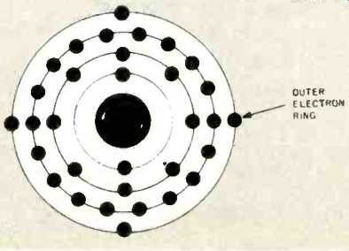
Fig. 1--The outer ring structure of germanium has four electrons.
A pair of germanium electrons form a stable atomic union by sharing their outermost electrons--four electrons from one atom, four from another. Thus the requirement for a total of eight is satisfied. Since atomically bonded atoms of germanium have no further need of electrons, any electron current trying to move through pure germanium will have its problems--it isn't wanted.
An element such as antimony has a total of five electrons in its outermost ring. If this element is added to germanium or silicon, a process known as doping, atomic bonding will take place, just as in the case of pure germanium or pure silicon, but now electron bookkeeping comes to our rescue. Antimony's five outer ring electrons plus germanium's (or silicon's) four, makes a total of nine, one more than is needed.
Germanium or silicon, doped with antimony, has an electron surplus. The germanium (or silicon) is no longer an insulator but has acquired some conducting properties--certainly not as good as silver or copper--but much better than originally. While it is called a semiconductor, this does not mean to imply it is precisely halfway between a good conductor, such as silver, and an insulator, such as glass. The antimony is a donor material, for through its generosity, it has not only contributed the four electrons required by the semiconductor atoms, but one electron in excess for each antimony atom. Semiconductor material doped in this way is called negative-type, abbreviated as N-type, or simply N. Obviously negative type since each electron, no matter how supplied, carries a negative charge.
Unlike germanium or silicon which have four outer ring electrons, and antimony which has five, an element such as boron has only three. This electron deprived element, as in the case of antimony, germanium, or silicon, would prefer having eight outer-ring electrons.
When this substance is used for doping germanium or silicon, the result is an atomically bonded pair which has only seven outer ring electrons--four from the semiconductor element and three from boron. Again, the properties of the germanium or silicon are changed, from a good insulator to a substance which has current carrying capability.
Semiconductors doped with a three electron outer-ring element are called positive type, P-type, or simply P, to indicate the existence of an electron shortage.
The Semiconductor Diode
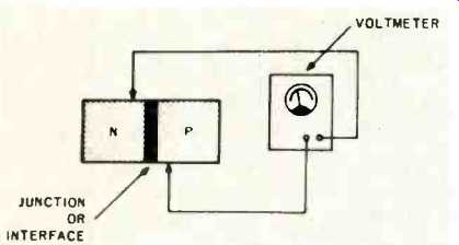
Fig. 2--A small, but measurable voltage, exists across the junction of the
two semiconductor blocks.
We now have available two blocks of semiconductor material: P-type and N-type; one with an electron surplus, the other with an electron shortage.
When these two are made to butt against each other as intimately as possible (Fig. 2), a small, but measurable voltage will exist between them. Some small movement of electrons will take place at the junction or interface, with electrons traveling from the electron rich or N-type over to the electron deprived or P-type. Once these electrons have migrated, they will join the semiconductor atoms at the junction, but as soon as they have their outer rings electron satisfied, they will block the passage of any further electrons, acting as a barrier for all the unsatisfied, electron-hungry atoms behind them.
Semiconductor Electron Movement
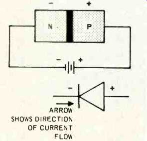
Fig. 3-A battery placed across the semiconductor diode overcomes the potential
barrier block (A); diode symbol (B).
To force electrons through this self-imposed barrier, a small battery can be connected across the P-N combination, as in Fig. 3. The minus terminal of the battery is wired to the N block; the plus terminal to the P block. Electrons will now move from the crowded minus electrode of the battery into the N-block, creating such an electron jammed condition in it, that numbers of them will force their way into and through the P-block. Since the positive terminal of the battery is a region of far fewer electrons, a place where they will not suffer the nearness of other electrons, they continue moving toward this terminal.
The end is not in sight, for they move through the battery, arriving at the negative terminal. And so the whole current flow process continues.
Forward Biasing
The battery used in connection with the two semiconductor blocks is called a forward biasing battery, but there is no relationship between this battery and that used for control grid bias in the triode tube. With forward biasing, current moves, as usual, from minus to plus, but there is no current control--as yet.
Reverse Biasing
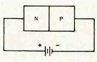
Fig. 4-Very little current flows.
It is only when the leads to the semiconductor blocks, (Fig. 4), are transposed that the true nature of what we have becomes evident. The generous through the reverse-biased diode, current supplied by forward biasing drops to a trickle. What we have is diode behavior since current flows much more readily in one direction than the other.
The semiconductor diode, then, made of two blocks of germanium, or silicon, N-type and P-type, permits the flow of current in one way, opposes it in the other. This means that whatever the tube diode can do, the semiconductor diode can do. The great advantage is that no heating current is needed; further, since the two blocks are in contact, the forward bias, equivalent to anode voltage, is much smaller.
The A.C. Biased Diode
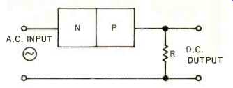
Fig. 5--The semiconductor diode can be used as a rectifier or demodulator.
The semiconductor diode can be used as a rectifier or demodulator, changing a.c. to d.c. as in Fig. 5. When the a.c. voltage source has a forward-biased polarity, current flows through the diode. When the a.c. voltage changes its polarity, the diode is reverse biased, and so current through the diode becomes negligible. If this current is allowed to flow through a load resistor, R, the voltage produced across this resistor will be d.c. Current flows through that resistor in one direction only. Except for technique, this is similar to the behavior of the tube diode. Further, the semiconductor diode can be used as a signal rectifier or demodulator, in somewhat the same manner as the tube demodulator (Fig. 6). This receiver circuit, a crude, elementary type, can pick up signals, but cannot separate or amplify them, an acceptable condition at one time with single station broadcasting, but intolerable today.
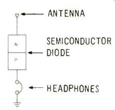
Fig. 6--The simplest receiver, even more so than the tube diode used in this
application.
The Transistor
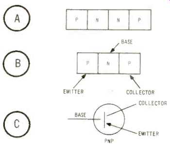
Fig. 7--The transistor consists of a pair of semiconductor diodes placed back
to back (A). The two blocks of N type semiconductor can be combined into one
(B). PNP transistor symbol (C).
The transistor, an amplifying type of semiconductor, consists of a pair of diodes placed back to back. Fig. 7 shows a pair of such diodes with the N-block of one in close contact with the N-block of another. The two N blocks can be replaced by a single unit, and so, reading from left to right, we have P-N-P. Since each will be working in a specific manner, they can be labeled as emitter, bass and collector, rather odd designations since the emitter doesn't emit, the base forms no foundation, and the collector doesn't collect. A rose by any other name, etc.
Transistor Current Control
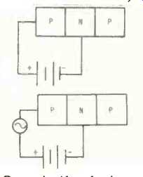
Fig. 8--One half of the transistor is still a diode and can be forward biased
as such (A). An a.c. voltage, placed in series with the forward biasing voltage,
will have the effect of varying the forward bias.
Although the two semiconductor diodes have been joined, with the base material common to each, they can still be treated as individual diodes. Fig. 8 shows one of these diodes, consisting of the emitter and base, as forward biased. In this arrangement, the collector block is momentarily disregarded.
Current control is obtainable by varying the amount of forward bias voltage. This can be done by putting a variable resistor across the forward biasing battery and taking off different amounts of voltage. The greater the forward biasing voltage, the larger the amount of forward current, comparable to putting more voltage on the anode of a tube. If an a.c. voltage is put in series with the forward biasing battery, the amount of forward current will keep changing in step with the changing a.c. voltage, depending on its polarity at the moment. When the a.c. voltage opposes that of the forward bias battery, forward current will decrease. And conversely.
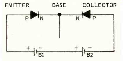
Fig. 9--The direction of current flow in this PNP transistor is from collector
to emitter.
The base and the collector form the second diode and this diode section is now reverse biased (Fig. 9). However, if the connection to the base is removed, it is apparent that both batteries, forward and reverse, are in series. Electrons will now move through both diode sections, in the arrangement shown in Fig. 9. If the connection to the base is replaced, a small current will flow through it, and so the current through the reverse biased diode will now be slightly less than the forward biased current.

Fig. 10--Basic PNP transistor circuit.
A small voltage change in the emitter base circuit results in a much larger voltage change across the load resistor in the collector-base circuit.
The whole action of the transistor revolves around the fact that a relatively small a.c. voltage-possibly that supplied by a signal source such as a radio station, record or tape player-is used to control the current flowing through the transistor (Fig. I0). If this current is allowed to move through a resistor, a voltage will develop across that resistor having a waveshape that is a reasonably good reproduction of that of the original signal voltage. There is one important difference, however. It will be much larger, that is, it will have a greater amplitude.
The action here is essentially the same as that obtained in the triode tube, except that the technique is different. In each case current or voltage is supplied by a d.c. voltage source--in the tube by a battery connected to the anode and in the transistor by a pair of biasing batteries. The current supplied by these d.c. voltage sources is made to vary directly in step with an a.c. signal. This current is then passed through a resistor and so the conversion process is completed. We start with a small voltage, control a current, and then convert that current into an equivalent, but much larger, varying voltage.
NPN and PNP
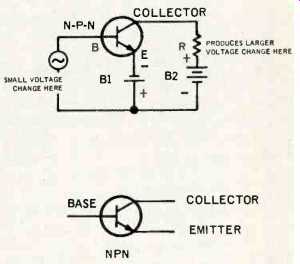
Fig. 11--The NPN circuit (A) is essentially the same as the PNP except that
the batteries are transposed. NPN symbol (B).
Unlike triode tubes, transistors form two basic groups: NPN and PNP. The only difference is in the way in which the original semiconductors are placed back to back. PNP and NPN transistors work in the same way, but to maintain proper biasing polarity, their connections are opposite (Fig. 11). In the case of the NPN, current flows from the emitter to the collector, while for the PNP current moves from the collector to the emitter. This is of no consequence to the output load resistor, for the amplified voltage developed across it is the same. All that is different is the polarity of that voltage.
(To be continued)
( Audio magazine, Oct. 1972)
Also see:
The Language of HIGH FDELITY: Part II--Basic Electronic Components (Jun. 1972)
The Language of High Fidelity--Part VII: The Basic High-Fidelity System (Dec. 1972)
The Language of High Fidelity--Part VIII (Feb. 1973)
Language of High Fidelity--Part XI (May 1974)
= = = =