1. Availability
As with the passive components the commercial producers offer a wonderful selection of semiconductor devices from the humble diode to large scale ICs. As enthusiasts our choice is limited only by our ingenuity in acquiring what we need.
Practically anything available in TH is made in SM also, but it will be prudent to find a supplier before rushing ahead with a particular design. A component may be listed in a manufacturer's catalogue and may be widely used but a distributor will often need to invest in a minimum order of 100s or 1000s so that we can buy one to play with. More and more ICs are being made in SM only and this will inevitably improve avail ability of SM types. In this section we will deal with discrete and integrated devices with the emphasis on their packages so the reader can become familiar with them. More detail on electrical characteristics is always available in manufacturers' data sheets. This is particularly important when power ratings are likely to be exceeded for example when transposing output circuits from TH to SM. Only the specialist will be concerned with the small differences in electrical performance. Overall there is good agreement between lead numbering of TH and SM devices, particularly the smaller ICs.
2. Diodes, Diodes, Diodes
It is astounding that the simple diode still plays such an important part in electronics. Its versatility seems endless and in SM you will find PIN diodes, signal diodes, switching diodes, rectifiers, full wave rectifiers, LEDs of all colors with clear or dif fuse lenses, variable capacitance diodes, zener diodes, voltage reference diodes, transient suppressors, hot carrier diodes (Schottky) and of course lasers. From a practical point of view we are saved total confusion by the fact that diodes have only two connections. But apart from a couple of standard packages there is less than perfect standardization.
The oldest SM diodes came in one of two cylindrical MELF (Metal ELectrode Face) packages. This package is totally sealed in glass and is therefore very reliable. They are in fact made by the same route as their TH equivalents. The only drawback is the difficulty in handling both by pick and place machines and hand soldering since they tend to roll off the PCB lands. A small slot in the PCB land will help prevent rolling.
The 1N4000 series of rectifier diodes come in this MELF pack age. Some small signal and zener diodes will also be found in the mini MELF package (Fig. 16).
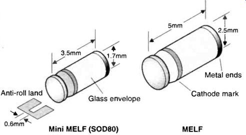
Fig.16 Structure of MELF and mini-MELF diodes
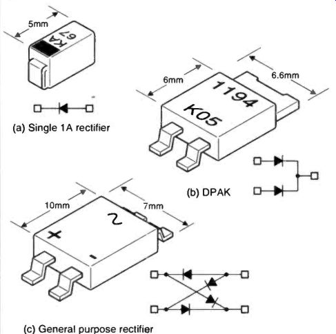
Fig.17 Typical rectifier diode packages--(a) Single 1A rectifier; (b) DPAK;
(c) General purpose rectifier
Various forms of anti-roll package are now far more popular for power diodes. Half-wave and full-wave rectifiers are made in a range of surface-mount flat packages. Fast recovery and other higher performance rectifiers are also found in such pack ages. Three typical formats are shown in Figure 17.
By far the most popular package for all small signal diodes is the SOT23. Versions of most types of diode will be found in SOT23 including switching, PUTs, SCRs, voltage reference, varicap, photodiodes and LED's. The connections are mostly as shown in Figure 18, but all possible connections are manufactured so a quick check with a meter might save a lot of problems if you are not certain of pedigree. Dual diodes are made in the SOT23 if one electrode is common. If two separate diodes are required the SOT143 package is used. Both these packages are ideal for hand-working.
Some less common packages include six terminals for switching diode arrays. Some half-wave rectifiers come in the SOT89 package which we will cover later. A useful range of LEDs and photodetectors are made in the very tiny CR10 series of packages, which are stackable and measure only 3-mm by 1-mm.
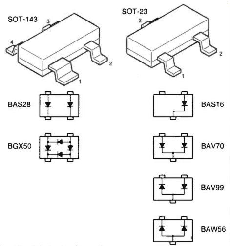
Fig.18 Diode configurations
3. Transistors
Transistors are manufactured in a beautifully simple set of packages and they have very good standardization of pinouts.
These packages are SOT23, SOT143, SOT89 and SOT223 and there will be a few oddities of course. The absolute universal outline is the SOT23. This is small but after a little practice in hand working it is quite manageable. Even for those who want to go for ultimate miniaturization the SOT23 will not be the limiting factor. It is an excellent optimum design in all respects, electrical properties, size, and power dissipation. All the familiar small signal devices will have equivalents in SOT23 or as near as makes no difference. The SOT23 package has a power dissipation capability of up to 200mW. The essential, typical, measurements are given in Figure 19. The SOT23 package has been around for some time and when we focus in closer on it we find some slight variations in its dimensions by different manufacturers. For hand working these are all inter changeable but it explains some visual differences which you may find. The TO-236 and SC-59 are both referred to as SOT23 but their dimensions are minutely different.
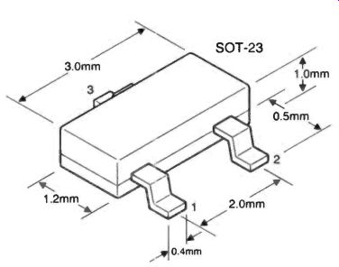
Fig.19 The SOT23 transistor package
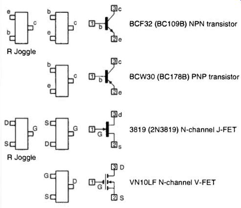
Fig.20 Some examples of SOT23 devices
Common devices from the TH world are sometimes given the same or similar type numbers in SM but in most cases special type numbers are used. Most devices are marked with a manufacturer's code rather than the type number for example the BSR58 FET is marked "M6". It is a good policy to record these for reference as you come across new ones, it will help if you have a mix-up. Typical connections to some common devices found in this package are given in Figure 20. Connections can not be taken for granted so check with manufacturers' data sheets, suppliers' notes and so on. In particular the base and emitter can be reversed, this is referred to as an "R" joggle and the type number will have an 'R' subscript. As an example the BCF32R in Figure 20 will have the code D77 as opposed to the standard BCF32, marked D7. Unfortunately different manufacturers can have different codes, those above refer to Philips devices. On the subject of pin numbering, there is some scope for confusion. The convention is to count anticlockwise when looking at the top of the device. Some manufacturers show a bottom view of the SOT23 package which seems pointless for an SM component.
Where a fourth output connection is needed, the SOT143 package is used. Again the Japanese SC-59 version and the TO-236/5 versions have marginal dimensional differences which are of no consequence to the hand user. Like the SOT23 variants the higher standoff versions (0.1mm) allow pcb cleaning fluids to penetrate under the casing to remove flux residues.
An excellent and well known example of a SOT143 device is the dual-gate MOSFET BF998. Newer devices include the GaAs FETs type CF730 and CFY39, the CGY50 GaAs MMIC and the BCV61B/BCV62B NPN/PNP matched transistor pairs.
Power dissipation up to 400mW can be handled with the SOT143 package. Dimensions are given in Figure 21.
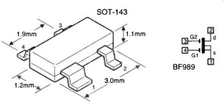
Fig.21 The SOT143 semiconductor package
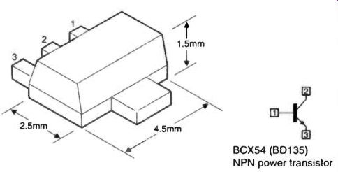
Fig.22.
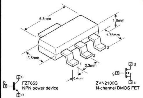
Fig.23 Details of the SOT223 package
Surface mount power devices start with the very well standardized SOT89 package. It will dissipate typically 1 watt but higher values have been quoted for recent devices. The heatsinking ability of the PCB, the area connected to the collector, is all important for maximizing power dissipation.
Dimensions for SOT89 package are less varied than the SOT23 or the SOT143. Examples of popular devices in SOT89 are the BCX54(NPN) and the BCX51(PNP) which are SM versions of the very useful BD135/BD136 complementary pair. Useful RF power amps are the BSR40, BFQ19 and BFQ17. The BST80 is an N-channel enhancement mode DMOS V-FET.
Two new power packages are now beginning to supplement the widely used SOT89 package. First, the SOT223 package fills the 1.5 to 2 watt range with bipolar power devices like FZT653(NPN) and the complementary FZT753 and the usual array of V-FETs, Darlingtons and so on. This is a very useful package and is a little more forgiving for hand working than the SOT89. The power rating assumes a line PCB for Rth(j-amb) of 60°C/watt and a 1.5in^2 PCB will have a sinking capacity of 50°C per watt. The sight of SOT89s over-dissipating and going for a swim in solder is not unknown. The SOT223 package gives the experimenter a bit more headroom in this respect. The second package is in fact older than the SOT223 but has been adopted as the main big power package. Originally it was described as a 2 watt device but it is now fully developed and devices capable of handling 20 watts can be found. There is considerable variation in D-PAK dimensions. This lifts SM well out of the small signal domain, what more could you need.
To end with, how about the PSD package, the 2SK2042 N-channel MOSFET in PSD will take 450V on the drain and dissipate 35 watts.
Fig.24 Details of the DPAK power package
Some new transistor outlines are worthy of mention, in particular the UMT (Ultra Mold Transistor) which is about two thirds the size of the SOT23 package at 2mm by 1.3mm. But the ultimate is the EM3 outline measuring only 1.6mm by 0.8mm or 1.6mm by 1.6mm including the gull wing leads. A number of special-function transistor arrays in multi-lead SOT23-like packages include digital transistor arrays.
4. Integrated circuits
Surface mount IC packages have settled down to a manageable number of types. Even so the constructor will come across odd-ball packages and variants on what we can regard as the industry standards. The simplest packages are the SOIC range, Small Outline Integrated Circuits. These are made with 8 to 28 pins, depending on the complexity. The pins themselves have evolved for SM application. Three types of lead have received varying degrees of acceptance during the development of ICs generally. By far the most common lead type is the gull-wing with many years of reliable service (Fig. 25).
The gull-wing lead, bends downward from the IC body to the PCB level and then outwards forming a lap joint. It is fine for hand-working, with its extended solderable area. The visibility is very good so that the soldering can be readily inspected and voltage measurement is easier with a suitable probe. A disadvantage of this lead is the larger device footprint required to accommodate the extended leads. Co-planarity errors can be a problem in automatic soldering but is of little importance for hand working unless the leads are badly bent out of true. The "J" lead takes up less space but the IC packages tend to be bigger to accommodate the lead itself. Visibility and inspection are difficult. The tendency is for J leads to be used for PLCC chips but the use of finer gull wings seems to be the way things are going. The "I" lead is persisting in the race for supremacy but only just. It has good strength and is quite compact but the leads must be sheared to the same length and the bare metal of the shear must be tinned otherwise it would not meet solder ability standards. The gull-wing is therefore our preferred configuration and in fact most devices used by the amateur will be of this type.
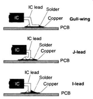
Fig.25 SMT IC leadout configurations
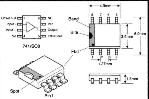
Fig.26 Surface mount version of the 741 op amp
Our favorite linear and digital devices, the building blocks for small projects, are supplied in SOIC packages. This includes the standard digital devices like the 4000 and 7400 series and a whole array of computer support devices. Also found in this package are the 555 and similar timers, the NE564D phase lock loop, all types of op amp, DAC/ADC, etc.
An important variant is the SOIC Wide package where the die won't fit in the standard SOIC. This has the same 1.27mm pin spacing but a wider body and type numbers sometimes contain the /W (wide) or /L (large) subscript. The popular 741 op amp is housed in an S08 package, Figure 26. Our first objective is to find pin 1 and there are plenty of clues. Looking down on the IC you will note one edge has a flat, putting this on the left places pin 1 on the top left. Pin 1 is sometimes indicated by a small circular indentation on the top left. The pin 1 end is very often indicated by a small semicircular bite at that end. If all this fails a white stripe may be found across the pin 1 end. It is common to find all these clues on one chip.
The smaller packages, up to S016 can be standard or wide but the larger packages, S020, S024, S028 and S032 are all wide packages. S032 and below have pin spacing of 1.27mm but the 40 and 56 pin VSO (very small outline) devices have a narrower pitch of 0.76 or 0.75mm and different package dimensions.
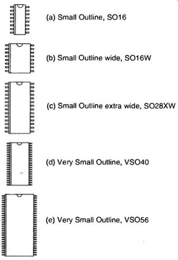
Fig.27 Some
examples of surface mount IC packages (a) Small Outline, S016 (b) Small Outline
wide, SO16W (c) Small Outline extra wide, SO28XW (d) Very Small Outline, VS040
(e) Very Small Outline, VS056
More complex, large-scale integrated devices are supplied in a variety of PLCCs, Plastic Leaded Chip Carriers. Typical devices which are well suited to this format are the AD720JP RGB to PAL encoder IC in a PLCC28 or the PD70325L 16 bit microprocessor in a PLCC84 package. The PLCCs have 20, 28, 32, 44, 52, 68 or 84 pins and J leads which can be soldered direct or inserted into PLCC sockets. The sockets are useful where a chip may be upgraded or for burn-in tests. In these packages pin 1 is identified by a small circle as indicated in Figure 28, and the pitch is 1.27mm.
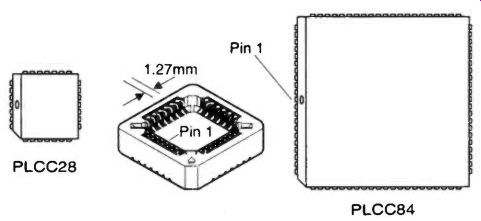
Fig.28 Plastic Leaded Chip Carrier IC and socket
The PLCC is quite bulky, particularly when a socket is used.
Conversion PCBs are available for SM to TH IC sockets if a socketed device is required. Much more compact circuitry is possible with the newer Quad Flat Pack ICs. QFPs can have very fine pitch, 1.25mm down to below 0.5mm. They are not so robust in handling but are very reliable once soldered in place. Such devices have gull-wing leads and are workable by hand with a little care. Service engineers have to cope with them and reworking has proved very practical. The usage of QFP is now widespread, a typical complex device is the DP83932 network interface controller in QFP132 package or the Z84C9008VSC Z80 CPU and support circuitry in a QFP100 package.
SMT is the target for continuing development and the odd new package can therefore be expected to intrude just when we get to grips with the existing standards. An example of this at the simple end is a whole set of single gate devices with type numbers in the BU4 series. The range includes NAND, AND, NOR, OR, INV, SCHMITT, and an analogue switch in a 5-lead SOT23 package. These are useful for supplementing existing logic ICs or for replacing discrete functions. Also, being very small the SOT23 gates can be dotted around the PCB just where they are needed saving the space and complexity of routing to a remote SOIC gate array package. These must be attractive to the experimenter as availability improves. In power devices there is a new DD package which seems to be mainly used for switching voltage regulators. This is a package similar to the DPAK, about lcm square and with 3 to 8 leads.
Fig.29 Quad Flat Pack, QFP package