1. Getting started
In this section we deal with techniques for development of circuit layout. To be successful at this, it is essential to have a feel for chip components. We therefore get round to meeting SMDs for real using a couple of simple projects. By now you should have a good idea of the range of SMDs available and outline descriptors like SOT23 and 1206 should be familiar to you. One or two sizes may also have imprinted themselves, in particular the 1.27mm SOIC pin spacing and the 1.9mm SOT23 base emitter spacing. Looking at pictures is all very well but the real world is a whole new ball-game and requires the acquisition of some skills in handling SMDs. At this stage I strongly recommend that you get some SMDs to play with. A couple of very simple projects will he described in just sufficient detail to get you started. Hand working methods will be covered in more detail later, when it will be better appreciated after a little practice.
The very small size and weight of SMDs result in some handling difficulties that may not be apparent from quoted dimensions and outline drawings. The first task is to come to terms with the almost microscopic size of the little beasts. If the code number on say a 1206 chip resistor cannot be read with the naked eye then some kind of visual aid will be needed to ensure that soldering is up to standard. Even those with perfect eye sight will feel the need for a small magnifier from time to time.
Do not underestimate the importance of lighting conditions as we are working at the limits of human visual capability. If you doubt this try reading the code on a 1206 chip resistor first in daylight and then under a 60 watt bulb at night. In the latter condition the eyes' iris is wide open and as photographers will know this reveals all the imperfections of the lens and diminishes the depth of field. Many people with what would be regarded as quite good eyesight cannot read chip codes under artificial light. Daylight is the number one top of the shop as a light source. The optimum conditions are inside a north facing window, in daylight of course. Unfortunately most of us must work in dark winter evenings and so artificial light and optical aids are needed. The first requirement is therefore plenty of light at the work area. This is best provided as a mixture of good background light in combination with one or two spots or desk lamps. Positioning a light source can be a problem due to specular reflection. A light source off to one side is often better than if placed right in front. The most annoying reflections occur if the light forms a 45 degree angle at the working surface area in front of you.
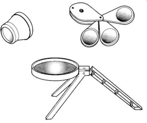
Fig.30 Selection of handy magnifiers for SM work
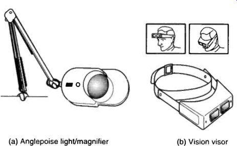
Fig.31 Wide field vision aids for prolonged use---(a) Anglepoise light/magnifier
(b) Vision visor
There are many different magnifying devices which are a great help to the surface mount constructor making 1206 work easy and extend our capability to the really tiny 0603 or even 0402 scale. Some typical devices can be seen in Figure 30. The triple magnifier is particularly useful and such devices are obtainable from watchmaker and model maker suppliers. A "+4" diopter hand lens with a handle which converts to a tripod stand is a real help for layout design at a low cost.
More complex visual aids which are handy for longer working sessions include stereo visors and Anglepoise lamp/ magnifier combinations. These give a wide field of view and are actually very convenient to use. The back-light Anglepoise magnifier has the advantage of optimum lighting direction. Two examples of larger vision aids are shown in Figure 31.
Attempts to place a chip component onto its printed circuit board solder pads with unaided fingers will soon prove almost impossible. They are simply too small to get hold of with thumb and forefinger so tweezers are essential. In any case they must be held down whilst soldering. The whole chip approaches the soldering temperature and would burn the fingers. Select the tweezers well, they must be of good quality and accurate at the tip. If they have any misalignment the chips will flick out of control and the only way to find a wayward chip is with a vacuum cleaner. Try finding a black-bodied SOT23 at the bottom of a carpet pile. You will quickly find the disastrous effects of a magnetized pair of tweezers. Many chips have ferromagnetic leads (nickel content) and will fly towards a magnetic tweezers' tip and stick to it with great tenacity.
Stainless steel tweezers are a must but some grades can become magnetized. A tape head or other type of demagnetizer can be useful. Ceramic tipped tweezers are an excellent alternative.
There are ranges of tweezers which are specially designed for SM work. These are expensive but the precise construction makes them a delight to use. The lightness of chip components gives us a further headache in that the slightest force or movement of the circuit board sets them out of alignment at best and at worst sends them flying off the board never to be seen again.
A stable working environment is therefore essential. It is useful to construct a small work station about 30cm square and edged with some beading to a height of about 1.0cm. Standard or high density chipboard can be used for this and for the perfectionist an antistatic laminate surface with stud connector and four small rubber feet will complete the job.
2. Ugly construction
We are about ready for a little hands-on experience with SMDs.
The first project is as simple as they come and we will use the most basic form of point to point construction. Actually this cheapskate method is very tedious and fiddly and really not SM at all. It will nonetheless help to focus the mind down to SMD level and show them at their worst, from here on it gets easier.
If you find this physically impossible to make, don't give up.
The proper printed circuit techniques described later are certainly a lot easier. The schematic shown in Figure 32 is for a static detector using an N-channel FET. If a statically charged object is brought near the gate of TR1 the LED changes in brightness. A 9V supply such as a PP3 battery is required.
Resistor R1 protects the gate from high discharge currents. A resistor from the gate to OV would seem normal but the circuit works well without it as a practical value would need to be of the order of 100Mohm for the small charges/high voltages we are trying to measure. You might try stringing a few 10Mohm chips together to reduce the sensitivity if required. C1 de-couples the supply and acts as an anchorage for R2 and the FET drain. The types of component specified are in no way critical and you should use any type of N-channel FET or LED that you can get hold of. The top view of the LED and TR1 shown in Figure 32 may not be correct for your chips but this is simply checked out in the usual way.
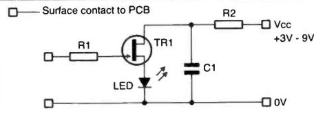
Figure 32
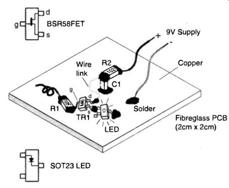
Fig. 33 Ugly construction of static detector.
Component list for static detector (Figure 32) Resistors R1 R2
Capacitor C 1k5 1206 chip resistor IMO 1206 chip resistor 100nF/50V 1206 ceramic chip capacitor Semiconductors TR I BSR58 SOT23 N-channel FET.
LED BY 100R SCYT23 general purpose LED
To put this lot together, select a small piece of PCB about 2cm square and make sure it is clean. A coating of flux from an aerosol will help if available. Use a standard soldering iron with the smallest tapered bit to hand. One problem with this ugly construction is the heat sinking capacity of the copper ground.
A very small iron tip may not be effective and a compromise between power and fineness is called for in this case. Pick up the LED with the tweezers and solder the cathode to the ground plane, Figure 33. Yes this is a very delicate operation and now you see why good tweezers are essential.
Now solder the source of the FET to the anode of the LED, this is a little easier. Solder the 100nF capacitor, C1, to the ground and link it to TR1 drain. To the top of C1 solder R2 and to the gate of TR1 solder R1. TR1, R1 and R2 therefore hang in mid air. A couple of cm of wire connected to RI acts as a pick-up. Now solder a short length of wire to R2 for connection to the positive supply and make a connection to the ground plane for the 0V supply. The ideal wire for the link and pickup is the fine Kynar wire used for wire wrap. The supply wires can be those of a standard PP3 connector. The current drawn from power supply should be a few milliamps if all is well.
3. Protoboard construction
To make life bearable a more effective form of construction is essential. A protoboard is the simplest viable method of circuit fabrication with SMDs. There is at present no type of stripboard which is suitable for SM use. Standard 0.1" stripboard could be used for passive components with not a little ingenuity--anything is better than ugly construction. But real difficulties arise with active devices, SOICs with their 1.27 mm pitch means that the strip is twice as wide as we would like and impossible to use. A protoboard is therefore required and your simplest approach is to get someone to run off a couple of copies of the one shown in Figure 34. But if you wish to be self sufficient, the simplest of PCB making equipment will suffice.
Photocopying onto acetate film and making a sandwich of the three copies in register will give a dark enough photopositive to work from. The method of going from a printed design to a real live circuit is described later. The layout shown may not be optimized for your needs, and it is an easy matter to design your own protoboard to suit the type of work in hand such as digital, analogue, RF, and so on.
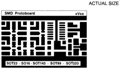
Fig.34 Track pattern for a universal SMD Protoboard
For a general purpose protoboard, some standard SM footprints can be obtained from a transfer sheet. A basic approach would be to set down a few SOT23 and SOIC pads along with plenty of 1206 pads. There is no spotface cutter as with strip board so gaps have to present in the design and inter-component links can be made with fine Kynar wire. Zero ohm jumpers should be used where possible. They make excellent linkers as they are neat and have very low resistance and inductance. This Kynar wire is available in several colors which can be useful for identification purposes. Quite complex circuits can be put together by using several boards for separate functions. On the other hand the unused areas of the protoboard can be cut off, making a small compact circuit if required. The protoboard design shown in Figure 34 is intended to minimize the number of links required. This was designed on a simple CAD system and the pads are somewhat larger than those from a transfer sheet so as to ease hand soldering. Referring back to Figure 3 you will notice that the SOT23 device can be connected in any orientation to accommodate joggles and other pin variations. Also, an electrode such as the collector is inevitably a nodal point where several connections are required. Typical collector connections are a load resistor and a coupling capacitor output, i.e. three connections. However, several links will be required for most circuits. Let us now implement the static detector using this protoboard. We are still using the same soldering iron and solder as for TH construction. Silver solder and other refinements will be introduced later.
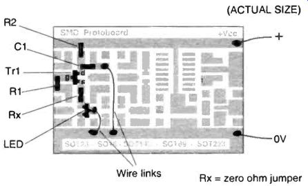
Fig.35 Static detector constructed on a Protoboard.
The first job is to decide on what goes where. To do this the chips can be placed on the protoboard and just moved around with the tweezers until a suitable layout, with minimal links, is achieved. Don't spend too much time on this, it's not at all critical and it would not matter if everything was connected by links. Some Kynar or similar 30 swg tinned wire is essential as it is unlikely that all elements can be interconnected without a couple of links. Having decided on a layout it is now necessary to solder in the chips. To do this, gently press the chip down to the PCB with the tweezers tip and solder one end to anchor it.
Subsequent contacts can now be made without it moving around. Start with the LED as before and work through, finally adding any wire links. One possible finished version of this circuit is shown in Figure 35, just two links are needed and an 0805 or 1206 zero ohm jumper denoted Rx.
At this point the magic of SMD should begin to dawn on you. You have just put a working circuit together without any drilling, having to turn the board over to solder, or snipping off pigtails. Including the time to get the chips out of storage, waiting for the iron heat up (starting with a ready made protoboard) this circuit can be running well within 10 minutes. The speed and simplicity of SM construction is surprising and from this point you may never look back. This exercise was aimed at getting the constructor attuned to the small size of SM chips and to some of the consequences of this. The art of SM construction does not stop here. There is much to be learned and it actually gets easier as experience is gained. It will be necessary to retrace areas like chip control and soldering in more detail later. Designing your own custom PCB is the obvious way forward.
4. Direct PCB design
The amateur is well supplied with materials for PCB design and production. Although this is primarily aimed at leaded components the principles are very similar and we have everything we need to produce excellent surface mount boards. To arrive at an etched PCB ready for population there are two main options: the layout design can be drawn "directly" on the PCB or a photopositive transparency can be used with UV sensitive PCB.
Putting the design straight onto the PCB is just about practical for SM but care is needed. Both processes are summarized in Figure 36. The direct method of PCB production is the least expensive, requiring little capital equipment. The price to pay for this easy entry, apart from the fact that it is very fiddly, is that it's a once-only process. The whole design must be redrawn if a second circuit is required or if the etch goes wrong. Similarly if a modification to the design is needed you must go right back to the beginning and redraw it. Even so it is more practical than with a TH circuit where the holes would need to be drilled again. At the high tech end, once set up for producing positive transparencies on a computer system it is a simple matter to run-off a modification. In order to demonstrate the flexibility of SMDs and to encompass those who don't have a computer system I will start with this very basic direct method of PCB production.
------------
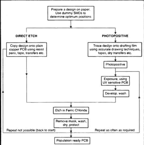
Fig.36 Options for manual production of PCBs
Prepare a design on paper.
Use dummy SMDs to determine optimum positions
DIRECT, ETCH
Copy design onto plain copper PCB using resist pens, tape, transfers etc.
Trace design onto drafting film using accurate drawing techniques, tapes, dry transfers etc.
Photopositive Exposure, using UV sensitive PCB Develop, wash Etch in Ferric Chloride Remove mask, wash dry, protect Repeat not possible (back to start) Repeat as often as required Population ready PCB
-----------
The first objective is to produce a rough pencil sketch of the layout on paper where it can be knocked into shape and the optimum component positions found. A suggested approach is based on designing a new kitchen where scale models cut from paper can be used. First draw a schematic of the circuit in question. It is useful to keep a few SMDs to use as dummy components for designing layouts. Start a surface-mount junk box, it soon builds up and storage space will never be a problem. Place the chips on a piece of paper in roughly the same positions as in the schematic, but suitably scaled down.
There is a tendency, at this stage to go for maximum miniaturization. Try to avoid this until you are more experienced as it will create soldering and etching difficulties. Using a fine, 0.3mm, propelling pencil, mark a line at the ends of each chip.
Remove the chips and convert each line into a rectangle forming the solder pad. This is pure guesswork (art) but it will be obvious that sufficient land must protrude out from the chip for the soldering iron to make good thermal contact. SOICs are treated similarly, just place a dot at the end of each pin, filling in as rectangles later. SOICs are tricky but it can be done.
Running tracks under 1206 chip resistors and capacitors is quite practical. Running tracks between SOIC leads is really not for the beginner, especially when drawing by hand. Even with computer artwork such lines are so fine as to create problems in etching. Having created a layout on paper with pencil and rubber it must be copied onto the copper PCB. A visual aid such as a 6" focal length stereo vision visor is very real help for all stages of manual PCB design. Hand drawing an SM track design into a copper PCB poses one main problem, that of making the track fine enough. The most basic approach is the famous Dalo pen. As supplied the tip is much too coarse and it must be pared down to a fine point, about 0.5mm, with a sharp scalpel. Simple circuits may not need a paper sketch and you could design the layout directly on the copper. The procedure for this is illustrated in Figure 37.
Place each chip on the copper surface and draw a line as on the paper layout. When the two end lines are made, remove the chip and fill out to a suitable sized solder pad with the modified Dalo pen. A transparent ruler can be used for straight lines including tracking between pads and with a little practice quite neat looking work can be produced. Fine overhead projector pens for permanent drawings on acetate film work well on copper and can also be used for this function. Etch-resistant tapes and acid-proof dry transfers are useful alternatives. The 0.031 inch tapes can be used for SOIC leads on 0.05in (1.27mm) pitch. Finally check the resist areas for pin holes and scratches and patch up where needed with the Dalo pen. The board can then be etched in 30% ferric chloride solution (1 part, plus 2 parts water) in the normal way at about 50°C with continuous agitation. It is then washed with water and thoroughly dried. The resist is then peeled off, removed with acetone (nail varnish remover) or otherwise. The copper should be rubbed down and polished with clean cotton-fabric, tissue paper or a proprietary polishing block. Mild abrasive cleaners for domestic use will remove the etch resist and polish the copper surface. To preserve the solderability, a coating of flux from an aerosol spray will suffice.
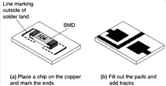
Fig.37 Drawing a circuit design directly on the PCB (a) Place a chip on the
copper and mark the ends (b) Fill out the pads and add tracks
4. Designing a Photopositive
Hand produced, 1:1 life sized, artwork on UV transparent, drafting film, is by far the preferred low tech approach. We will therefore look at this in more detail. It is still very much an artistic method, dimensions being obtained directly from the actual chips. We will get more quantitative later when computer design is considered. This hand made master artwork can be used to run off any number of copies and can be extensively modified to accommodate design updates. This is probably the lowest entry level for serious quality work. Some small investment is required but the benefits outweigh this.
Producing a master starts with a paper sketch, as above, which is then used as a tracing guide. The drafting film is then fixed over the paper sketch and the final very neat artwork is produced from it. This will be of a much higher standard than the direct PCB drawing because precision drawing pens can be used and they need not be etchant proof. A drawing could be made directly on drafting film but the paper intermediate obviates corrections to the final artwork. A practical project will be used to illustrate the procedure. This is a useful little audio output stage with flexible parameters, with many uses such as a signal tracer or radio output. The circuit is shown in Figure 38.
The LM386 IC is well known and the connections to the SOIC/S08 and 8 pin DIUTH versions are identical. By altering the components between pins 1 and 8 the gain can be tailored to requirements. With pins 1 & 8 NC, i.e. no external components, the gain is X20. With the 1.2k and 10-uF components shown the gain is X50 and if a single 10µF capacitor is used the gain increases to X200. Provision is also made for input variation such as capacitive coupling or direct coupling.
The data sheet should be consulted for more information on frequency response and so on. Note, I have adopted the use of small squares for connections to the circuit to symbolize that wires will be soldered to surface pads. The components marked Rx are zero ohm jumpers and are a great help for jumping tracks and keeping the finished circuit board neat. They are also more reliable than wire links and much easier to use.
Components list for Audio Amplifier (Figure 38)
Resistors
R1 10R 1206 chip resistor
R2 1k2 1206 chip resistor or OR for high gain option
RX 0R0 Zero ohm jumpers
Capacitors
C1, C4 100nF/50V 1206 ceramic chip cap (2 off)
C2 50nF/50V 1206 ceramic chip cap
C3, C5 47µF/16V tantalum cap (2 off)
Semiconductors:
IC1 LM386 in SOIC SO8 package
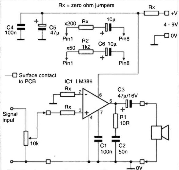
Fig.38
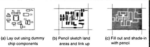
Fig.39 Development of a PCB track pattern----(a Lay out using dummy (b) Pencil
sketch land (c) Fill out and shade-in with pencil chip components areas and
link up
A universal audio amplifier
To create the pencil and paper layout design use some scrap components as dummies and lay them out as in Figure 39(a) This may take a little time as interconnecting tracks have to be kept in mind and links and under-runs kept to a minimum. A first approximation to the layout can be almost identical to the schematic diagram. This can then be stretched here and there to account for actual size of the components and to achieve an even distribution of chips on the PCB. If the components end up crowded in places, it is probably not the best layout. Don't try to make the circuit too small as plenty of pad area makes hand soldering much safer. It is good practice to make power rails as thick as possible. Even with a generous layout an SM circuit will still be very small and of course the profile is not much thicker than the PCB itself. Surface mount gives us a great volume reduction even if the area is not fully shrunk. Use a 0.3mm propelling pencil to sketch out the pads at the chip ends and SOIC leads. This is illustrated in Figure 39(b). Draw in the interconnections as fine lines. Now fill out the tracks keeping as much copper on the board as possible. A light shading with pencil helps to define the tracks. You should end up with something like Figure 39(c). Keep testing the drawing by matching up the chips and don't worry if ample use is made of the pencil eraser.
Now for the precision stage. To produce the final 1:1 positive master you will need some drafting film, which is readily available. The key to success at this stage, notwithstanding any vision aids you may choose, is a fine drawing pen. You will need a 0.25mm Rotting Isograph or similar professional grade drawing pen. A bottle of black drawing ink is also needed. This pen is expensive but it will last if maintained properly and this means cleaning it regularly. A 0.35 mm pen is useful for filling in large areas and if you are pushing the barriers forward or into making bugging devices, a 0.18mm pen will make superfine masters. A scalpel and some small blades is required for corrections to the master. A Swann-Morton size 3 handle fitted with No. 15 blade is just fine. Obviously a UV light exposure unit is essential, although sunlight works to some extent. Doing a bit of DIY on the exposure unit by adding a white 60 watt bulb makes an excellent back lighting unit for making and correcting the final master. I should not have to point out that a separate mains supply is needed to operate the bulb independently of the UV source. Staring into the UV will shorten your career in SM. Finally a professional grade stencil is necessary, particularly for drawing straight lines. The type supplied by art shops with electrical layout symbols is suitable, for example Rotring Art 852.762. This has tiny pips on one side to keep it slightly off the paper and an accurate cm scale along one edge which is very useful. We are now ready to go.
Cut off a piece of drafting film, about 8cm x 6cm for the circuit in hand. Draw an accurate rectangle, defining the edge of the circuit, on the final pencil drawing such that the lines project a little at the corners to act as registration markers or fiducial lines. Place the drafting film over the drawing and fix the top edge with some Pritt adhesive. Using your 0.25mm drawing pen and stencil, trace the lines around the edges including the corner projections so that if the film is moved it can be re-registered. Use a straight edge on the stencil for all lines. A good plan is to work down the drawing, copying the horizontal lines first. Then work from one side putting in the vertical lines. Finally draw in any tricky bits freehand. You should now have an outline drawing of all the landmasses. In this final operation the gap between tracks is set and must be kept sensibly wide. A separation of 0.5mm is comfortable whereas 0.25mm is getting a bit close and 1-mm looks like a barn door on this scale.
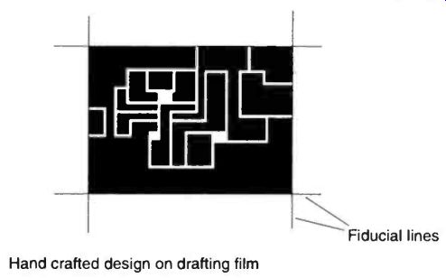
Fig.40 Photopositive for AF amp (actual size)--Fiducial lines; Hand crafted
design on drafting film.
The track areas can be filled in using the larger pen to flood in wide expanses. The ink can be dried from time to time on a radiator, especially if corrections are required. It is inevitable that the odd slip will create unwanted bridges or minor changes will be needed. The drawing ink does not penetrate the drafting film, but just wets the translucent surface coating and when it is fully dried the ink is easily scraped off with the tip of a scalpel blade. This is a delicate operation but with a little practice it will be found to be a most useful facility. You should now have a hand-made photopositive master similar to Figure 40.
The most difficult step in this manual process is the drawing of footprints for SOICs, SOT23 transistors and so on. A little further investment can greatly ease this process. A4 sheets of SMT dry transfers containing all the common footprints are available. These are made for 1:1 working and can even be applied to the PCB directly. The footprints are aimed at hand working, being a little larger than would be used for machine placement and soldering. The production of a master positive is now just a matter of deciding the overall component positions, popping down the required footprint from the transfer sheet and then adding the interconnecting tracks. The transfer sheet even contains suitable tracking. In practice I find this is very useful, giving neat professional results in a much shorter time than the manual method. The one slight disadvantage is that the design does not leave much copper on the board. I therefore use the transfers in combination with the manual method. The technique is to set down the complete circuit using transfers and then fill out the tracks with the Roving pen. Most of the pads can be expanded as they are quite small. This greatly eases manual placement and soldering of the chips. In some RF designs the more skeletal layout can be desirable but even in this case it is important to have as much ground area as possible. The ground and supply tracks can be filled out by pen, possibly the larger 0.35mm size. The transfer sheet is illustrated in Figure 41.
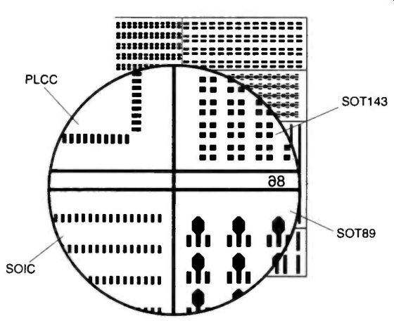
Fig.41 A4 sheet of dry transfer SMT footprints
A photopositive made by any of these techniques is quite robust and the drawing inks so far encountered have good flexibility. It is still good practice to check for pinholes and small cracks before use. This is done by back-lighting. An artwork light-box with an A4 viewing area (230mm x 380mm) and a white diffuser is ideal for this and, indeed, for preparing the drawing in the first place. Alternately a DIY version such as mentioned previously will suffice for this purpose and the trusty 0.25mm drawing pen will do the required patching up.
Manual techniques as described can lead to quite neat results.
The completed audio amplifier circuit produced from the hand crafted photopositive on drafting film is shown in Figure 42. But it is hoped that you will plough through Section 5 before you set to work on it.
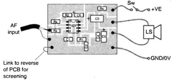
Fig.42 Audio amplifier component positions on PCB
6. Computer Based Design
Computer based PCB design systems represent the ultimate in speed and accuracy. New programs are appearing regularly and all of them boast SMT support. Happily the prices are realistic and hardware demands modest. Even the most basic 286NGA/9-pin matrix printer set-up will get you started. The older PCB design programs only offered limited built-in SMT facilities but they need not be dismissed. Most have the facilities to lay down rectangular pads of various sizes at the correct spacing and to link them with tracking which is the basic requirement. PCB design systems open up a world of facilities but these are better appreciated if based on some practical experience with manual methods. It is important for the beginner to relate to the physical world by printing out and matching up dummy components at regular intervals as the layout is developed. Designs are easily produced on the screen which would be impossible to use in practice. Typical problems are excessively fine lines, insufficient room to get a soldering iron tip to the pad and not enough space for component casings.
More advanced users can, of course, go from schematic to PCB with fewer test printouts.
The most obvious attraction of PC based design systems is their editing power. Images can be updated instantly without loss of quality and the whole design can be repeated several times on the same printout. Extensive symbol and pad libraries, which can be added to, save time and ensure consistency. Grid- snap or freehand mode allows placement of tracks and pads down to 0.025 or even 0.002-inch. The 0.05-in grid-snap (half of the 0.1in standard grid) is the 1.27mm spacing required for SOICs, ideal for SMT work. The smallest areas of the layout can be magnified with a zoom facility for such accurate placement, or for routing of underpasses. Pad and track widths can be altered over a wide range. Tracks can easily be placed between SOIC leads on the screen but in the real world this pushes the etching technology to the limit and is probably best avoided. Digital system design is made easy by track repeat facilities.
A great advantage of SMT is the capability of double-sided construction leading to even more compact circuitry. Most PC systems offer this facility, but of course small projects will seldom warrant the extra complexity. Solder mask and silkscreen layers are an attractive facility for small run offs.
When working with PC systems it is possible to approach a layout design with dimensions firmly in mind. This contrasts with the manual methods, especially when working at the 1:1 scale, where pad size is very much a matter of subjective judgment. Of course it is possible to operate the system in a trial and error fashion but after a little experience the advantages of an objective approach will be apparent. In previous sections, chip dimensions were given to illustrate their small size, telling us little of the footprint requirements. In layout design, particularly with CAD systems, we are concerned with footprint areas.
The establishment of pad sizes suitable for hand soldering and a knowledge of chip component area demands, leaves only track routing to worry about. Schematic capture facilities on certain systems can help here and zero ohm jumpers can reduce the number of wire links.
Chip component manufacturers recommend footprint dimensions for hand soldering, which won't let you down, but I find it better to expand these as much as possible in a particular layout. Heavy reworking can dislodge fine tracks and excessively small solder pads from the fiberglass substrate. The formulations which exist for calculating land pattern sizes are a bit optimistic and not really applicable to hand soldering.
Typical chip component footprints for the more common devices are given in Appendix V. These are based on manufacturers' recommendations for wave soldering. For hand working these should be considered minimum and expanded where possible. For manual work with solder cream, use the recommended wave soldering dimensions given. When significant power dissipation is required the pad area can be an important radiating element. The copper rear side ground plane can also take some heat away. In most applications power devices can be adequately "heatsinked" with a square cm or so of copper, but if there is any chance of a meltdown, proper calculations are required. If certain circuit elements are heat sensitive, a suitable separation must be used or a separate circuit module may be needed. In any case a modular approach is very useful as small PCBs are easier to handle and updated units can be added as required.
As with manual drawing, attention to the gaps between conductors on a PCB is important and again 0.5mm is a safe rule for project work. The degree to which this can be reduced is dependent on your system for getting from on-screen to photopositive and how the UV exposure and etching is done.
One possibility for determining device placement is to set a clear area, or aura, associated with each device and keep it clear of other chips. In general the component density on a board should be arrived at by considering factors like clearances required for rework and repair, cooling requirements, accessibility for soldering and inspection of joints. Some rework tools require a disappointingly large access area, at each end of chip resistors for example. It is good practice to lay out components in parallel with grid lines. Arrange for services like V+, VO, input and output to be connected to pads at the edge or ends of the PCB. CAD systems cope well with hybrid circuits containing a mix of TH components and SMDs. Plated-through holes (PTH) are easily produced using small kits made for the purpose.

Fig.43 Live wire detector
To illustrate a computer based design we have another simple but useful project. This is a live wire and hash detector.
I find it a very useful addition to the DIY tool box. A couple of centimeters of PCB tracking acts as an antenna. It will detect where live wires are running in a wall and will trace sources of interference. It detects the 50Hz mains as well as any hash or spikes on the line and there is usually plenty. A visual indication is given by the LED which should be a bright one.
An audio indication is also produced on a ceramic sounder.
This is a high pitched tone for a strong mains signals but the switching is gradual and an indication of the type of interference can be heard. The circuit will draw about 15mA with all guns blazing. Sensitivity is adjusted with VR1 so that the LED begins to light up when the antenna is a few inches from a live wire. The device is very sensitive and the length of the pick-up antenna can be reduced if required. The sounder leads are carrying square waves and should not be too close to the antenna.
Components list for Live Wire Detector (Figure 43)
Resistors:
R1 10M 1206 chip resistor
R2 4k7 1206 chip resistor
R3 470k 1206 chip resistor
R4 220k 1206 chip resistor
R5 470R 1206 chip resistor
Potentiometer VR1 50k Type 3204 preset
Capacitor:
C1 100nF/50V (X7R dielectric) 1206 ceramic chip cap
C2 470pF ( C0G dielectric) ceramic chip cap
Semiconductors:
D1 BAS16 SOT23 diode
LED BR100 SOT23 general purpose LED
TR1 BCX19 SOT23 general purpose NPN
IC1 4069 CMOS hex inverter in SO14
Before producing a track layout for this circuit I made up a set of 1206, SOT23 and S014 footprints for 1:1 working and copied them onto the design as required. This was done on a standard PCB design package which had only a limited set of SM pads. For the 1206 footprints I selected a square pad, varient "C" on my system (Easy PC), and printed out a selection of pads of various widths. Matching up a 1206 chip resistor to the printout I selected pad width "12" which looked comfortable for hand soldering. The next job was to complete the footprint by adding the second pad for the other end of the chip. This was a matter of placing a second pad of the same size and fine tuning its position in freehand rather than snap mode.
A couple of print-and-try sessions was all that was needed. The SOT23 footprint containing three pads was designed in the same manner but based on varient "G" which is a rectangular pad. For this project a width of "7" was selected. The SO14 IC footprint has a pin spacing of 1.27mm which is half of 0.1" so that in snap mode "1/2" of the placement is automatically spot on. The only problem was to select a sensible size of pad with an adequate gap between the IC leads. Incidentally in designing the protoboard discussed earlier the length of the IC pads was important as sufficient area is needed for fine connecting wires to be soldered to each one. For present purposes the IC pads were made up of two varient "G" pads of width "6" placed end to end.
Fig.44 Skeletal (a) and filled out (b) versions of the live wire detector
PCB shown life size.
Having produced a set of footprints in a corner of the CAD screen it was a simple matter to block each one and repeat it in the required position. After all the footprints were placed, the tracks were added. Track widths were as wide as possible consistent with adequate gaps. A 1:1 printout was then made and dummy components laid in position. Using the block and shift facilities in freehand mode, tight spots can be relieved and a good layout produced in a few print and match up sessions. The first workable design produced by this method is a skeletal lay out as shown in Figure 44(a). This is quite practical with the advantage that chip component positions are easily identified. I have used many such skeletal PCBs without difficulty, but in keeping with the philosophy of leaving as much copper on the PCB as possible the spaces can be filled up by adding tracks and pads as required. The result is shown in Figure 44(b). In this case a small residue of the original footprints has been left so that the component positions can still be found.
This track layout has to be printed out and turned into a PCB which must then be populated. The input impedance of this circuit and the static detector circuit is very high and therefore glass fiber PCB is recommended. It is assumed that double sided PCB is going to be used but the reverse side copper should be removed from the pickup antenna area. If you intend to use this track layout it is hoped that you will plough through the next section on working with SMD's first as it is intended to be instructive and may help to get a better result. A component overlay based on the filled in version is shown in Figure 45 for convenience. Obviously it should be housed in a plastic box.
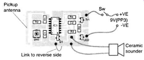
Fig. 45 Live wire detector component positions
The weak link in home computer systems is the means of producing a working photopositive of the track pattern. The first degradation is the printer itself in terms of head accuracy, print density and so on. This is particularly the case with the ribbon printers. Inkjet printers give very accurate reproduction with excellent print density. This can be further improved by selecting a paper which has been designed for inkjet use. Direct printing onto drafting film with matrix or inkjet poses drying problems and the density of the image is insufficient. The simplest practical solution is to run off say three photocopies of a paper printout on clear acetate film of the type used for over head projectors. Then cut out the images, leaving a suitable area around each. Next combine them in register using a little Pritt adhesive about I cm away from the business area. Some form of registration aid such as a fine line around the edge of the image is a big help. Sandwiching the photocopies increases the density of the image. Rotating the paper master in the photocopier between copies will ensure that imperfections from the copier cancel out. The 1% to 2% expansion produced by many copiers is not usually a problem, but some copiers expand more than this and expansion can be different across and down the page. Copying published artwork in this fashion is also possible. The quality of matrix printers can be improved by printing out the image enlarged, x2 or more, and then photo-reducing onto film. A small improvement in final PCB track quality can also be achieved by printing out the image reversed so that the print side of the photopositive must be in direct con tact with the resist on the copper.
Laser printing directly onto film can be successful. Many computer PCB design programs provide drivers for a plotter which is a very good method of getting a large image which can be reduced. It is also possible to get release paper which will transfer its laser printed or photocopied image directly onto a PCB using a hot iron. Yet another possible method is to spray a paper printout with "WD40" which makes it transparent to some extent and, with care, this can be used directly for UV exposure. Prolonged exposure is required with this technique.
Remember to be careful about using aerosols in confined spaces and be aware of possible flammability dangers. Always follow manufacturers' instructions and precautions. Moving up market, the design can be stored on disc for printing by a photo-plot bureau. Before continuing with the live wire detector, let's deal with some more practical matters.