1. Selecting the Substrate
Having produced a track pattern for your PCB, a suitable substrate must be selected. For the SMT professional this is a daunting task. Most of the problems concern mechanical properties such as thermal conductivity and thermal expansion coefficient, flexural rigidity and electrical characteristics like dielectric constant and RF losses. Such considerations lead them to choose a particular substrate from a wide range of types. Examples are fiberglass/PTFE for microwave use or alumina for military or potted engine management systems. Less accessible PCB materials include polyamide-fiberglass, polyamide-aramid, epoxy-aramid, polyamide-quartz, and various mixes of these. They have lightweight, very low thermal expansion coefficients and special dielectric properties.
A recent development consists of a thick aluminum base coated with an insulating layer onto which the copper is bonded. This has remarkable thermal conductivity and heatsinking properties. Inorganic, constrained core-based on copper clad Invar, compliant layer and flexible substrate will also be found. If you come across some odd looking PCB it may be one of these but it need not bother us for amateur construction. The choices for the amateur are to some extent made for him by availability, but one should be aware that this is a vast subject and if you are working with anything out of the ordinary, don't make too many assumptions.
The soldered joint, bonding the chip component to the PCB, is also its electrical contact. It is not surprising that this is a focus of attention for long term reliability of the circuit. During its lifetime the joint is subjected to mechanical stress and stress resulting from temperature cycling due to power dissipation and of course environmental temperature cycling.
SMDs are mounted very securely to the PCB. Any stresses in the board are therefore coupled into the chip. Such stress can arise from simply bending the board, for example by bolting it to an uneven surface. Also, if the PCB is tightly bolted to the equipment housing, any handling stresses will reach the PCB.
Electrical power dissipation in a chip component will lead inevitably to thermal expansion. This puts stress (force) on the joint which responds with stretch or contraction which is referred to as strain. At switch-on the chip heats up faster than the surrounding PCB producing an initial strain on the joint even with well matched component and substrate. Ambient temperature increase or decrease will result in strain if the component and the PCB have different thermal coefficients of expansion. A good example of the latter would be a ceramic chip on epoxy fiberglass which would only be reliable over a limited temperature range. If the strain on the joint exceeds the elastic limit of the solder then plastic deformation will take place and after a number of cycles the joint will fail. There are many other factors which can be considered in pursuit of circuit robustness. Well that's the bad news, but don't worry, it's not so bad.
Continual cycling of the joint within its elastic limit is OK.
Solders have a yield point approaching 0.5% so they will simply bend or stretch and fully recover up to this point. Luckily, chip components like SOICs and SOT23 discrete devices with gull-wing leads can also take some of the strain by slight flexing of the gull-wing. Leadless devices like chip resistors and capacitors are less forgiving, but they are so small that for most sensible temperatures the expansion is within the elastic range of the soldered joint. The compliance of the joint is maintained by using as little solder as possible consistent with making a good joint. As for mechanical stresses on the PCB it is a simple matter to arrange some compliance in the mounting yet hold it securely with plastic mounting pillars and so on. Also small PCBs will flex to a much lesser extent. I strongly suggest the use of double-sided PCB and keeping as much copper on board as possible. Most amateur projects will occupy only one side of the PCB in which case the copper screen on the unused side should be connected to the ground on the circuit side in one or more places. This can be done with Veropins or with snugly fitting wire links around the edge.
The above precautions must be pointed out for completeness so that if a critical situation arises the constructor is forearmed.
It must be said that in several years of work with SMDs as the only method of circuit fabrication, I never had a circuit failure due to mechanical problems, albeit most work has been with PCBs measuring less than 100 cm^2. I have also been surprised at the toughness of SMD circuits both hand-made and commercial, their indifference to abusive flexing and mechanical shock and to freezing both by nature and with aerosols. The reliability of SM circuitry is also apparent from our daily experience with consumer goods which just go on working.
The choice of easily available PCB materials is limited to SRBP in various guises or the ubiquitous fiberglass. The lowest cost materials are the SRBP paper based phenolic and epoxy reinforced composites. They have poor dimensional stability and poor flexural strength. The electrical properties are not so hot either and this is not helped by twice the water absorption of fiberglass. Double sided SRBP can be used for SM without problems but I have found that the single sided material warps badly and is probably best restricted to very small circuits. The epoxy composite material is available with a flame retardancy rating up to FR3 and is the best quality. But our old friend, woven fiberglass- epoxy laminate- is an excellent general purpose material and although it is sharply dearer than SRBP it is worth it for the peace of mind. The most popular grades are the GIO and the preferred flame-proof (FR4) material which is made to BS4584. This will run continuously at 130°C and will take whatever you throw at it for soldering. This board is 1.6mm (46") in thickness with a copper content of 305g/m2 (loz/ft2) and 0.0356mm (0.0014") thick per side. Thin fiberglass PCB of 1-mm thickness can be found and will save space if a very low profile circuit is needed. The flexibility of this material limits it to small projects. The double sided, standard 1.6mm, material is sometimes called 2 ounce thickness.
Cutting, sanding and filing this type of PCB material produces loose glass fiber dust which has a health risk, so take appropriate care. For most purposes positive working photo-resist pre-coated boards will be used. This is covered on both sides with a peelable crepe material or black plastic film which protects it from light and scratches in storage and handling. The sensitivity of this material to UV and its development time can vary considerably with storage, especially if the temperature goes above 29°C. The protective backing is removed from one side and the master artwork is placed in direct contact for exposure. The art is placed on the PCB with the ink/image side away from the resist layer. The image therefore faces the light source, unless you are working with a reversed image to improve resolution. Drafting film is translucent and needs more exposure to the UV than clear film. You can coat your own PCB with UV sensitive photo-resist using a proprietary aerosol spray. Good clean working conditions are required and the copper surface must be well cleaned beforehand. Home treated PCB has shorter exposure and development times but it requires some practice to get an even film thickness.
After exposure to UV the positive working photo-resist which is a blue-green color must be developed. On development the latent image initially appears as a darker color but soon dissolves to leave the unprotected copper. Fully sealed kits are available for PCB developing and etching and these can easily be used for SM work. The most basic home brew method is described here. The developer solution is strongly alkaline and must be handled with great care as it will readily dissolve skin.
If you do get a drop on your skin, wash the area under running water.
A proprietary developer will give consistent results but a simple home-made formula based on sodium hydroxide (caustic soda) works very well. This consists of about 1.2% caustic soda (weight/volume) for use with home-made spray-on resist or 1.6% for commercial pre-coated PCB. Development is at room temperature and should be complete in under 10 minutes, ideally about 5 minutes. Discard the developer after use. It could be stored for a short time in a sealed container. Plastic is better for this as it will tend to etch glass over time. Carbon dioxide from the air will slowly neutralize it during use.
The developed PCB must be well washed as any alkali carry-over will neutralize the acidic etchant, ferric chloride, and in fact it will precipitate undesirable iron compounds. A very gentle application of some abrasive cleaner will clear the mask residues from the narrow gaps between tracks and reduce the chance of copper whiskers remaining. The most convenient etchant for the copper is a solution of one part ferric chloride dissolved in two parts of water by volume. This is acidic and is corrosive to most metals including stainless steel. A plastic or glass container is essential. It will permanently stain most materials especially cotton fabrics. Etching is done at about 50°C and continuous agitation is essential--gently rocking the bath will suffice. Etching time depends on several factors but should be complete in about 20 minutes. The ferric chloride solution is usually stored for repeated use until it becomes very cloudy and obviously exhausted.
After etching with ferric chloride solution the board should be rinsed well. The mask should then be removed with stronger, 8%, caustic soda solution. The green mask should change to a more purple color and dissolve away. If some traces remain after a few minutes the PCB can be rinsed well and then rubbed gently with an abrasive cleaner to remove it completely.
Excessively strong caustic soda solution tends to make the mask less soluble.
The steps leading to the preparation of a population-ready PCB are just the same as for through-hole work. There may be a tendency to produce very fine tracks with SM and as all land areas etch sideways, in some circumstances the fine track could etch through. This can happen when there are large areas of land to remove and insufficient movement in the ferric chloride bath so that the process takes too long. Good solderability of the copper land areas is very important for SM work. For this reason some attention to the final preparation is useful.
After etching, wash off fully with clean water. If the copper is not perfectly polished then use a mild abrasive to ready it and rinse it off fully. Dry the PCB with paper tissue and then spray it with some alcohol or 1,1,1, trichloroethane PCB cleaner to remove any greasy deposits. Completely dry it in a warm place.
Finally, spray with a fine coating of rework flux from an aerosol. Harden up the coating by getting the board hot on a radiator for at least half an hour. The flux is based on a rosin derivative and its high static friction coefficient helps with control of the chip components during board population. You should now have a shiny well protected PCB with excellent solderability, ready for population. Roller tinning the PCB will also give excellent solderability, although the little solder bumps at the trailing edge of the solder pads can be a bit of a problem. These could be removed with solder wick but this is not usually necessary. Air knife and other more expensive methods leave a smoother surface for SM work. Chemical tin plating can be difficult to solder if not done correctly.
2. Working Conditions
A good working environment will go a long way to ensuring success in producing a neat looking circuit which performs its intended function reliably. You can start with just an iron and a little standard 40/60 solder but it will be useful to develop a more customized set-up. Good lighting and an array of magnifiers have been described and are a vital part of any SM set-up.
Other items will be mentioned as the need arises.
SMDs are packaged mostly in reels or magazines and occasionally in bulk or loose. The 18 cm diameter reels contain typically 1000 or so chip resistors, capacitors or active devices.
Small quantities will be cut from the reel as required. Full or part reels appear on the surplus markets from time to time, and the purchase of a reel of common values like 1-k resistors could be less expensive over time and certainly very convenient.
Components on the reel are in a paper or plastic tape containing small sealed individual cells as shown in Figure 46. Left in this form they will maintain their solderability for a long time.
Free components, open to the atmosphere will absorb sulphur and other compounds from the air reducing solderability. This would be a disaster for automatic production where all chips are soldered at once but for hand working where individual chips are attended to it is rarely a problem. In any case it is better not to handle chips if you can help it because salt and other constituents of perspiration slowly react with the terminations and reduce solderability. Resistors and ceramic chip capacitors tend to be in paper tapes whereas diodes and transistors tend to be in plastic tapes. In both cases the wells are covered by a continuous strip of clear plastic film. This is peeled off by the pick and place machine and as each component is exposed it is picked out with a tiny vacuum pick-up device and placed on the PCB. The orientation of discrete devices in a tape is not random but as required by the production machinery.
Magazines are used for integrated circuits, they have a variety of cross-sectional shapes to suit the chip. The length of the magazine is 50cm with a flexible plug at each end but they can be cut and plugged for small numbers.
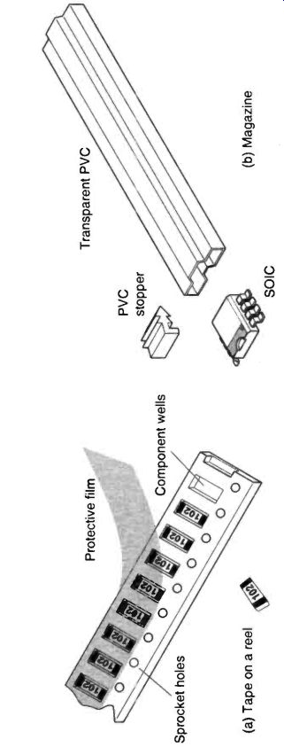
Fig.46 Tape and magazine chip packaging---Protective film Component wells
Sprocket holes (a) Tape on a reel.
SMDers have a strong interest in soldering irons and constantly search for the smallest tip on the planet. You will find that a clean, well tinned tip is more important than striving for fineness. Rule one is get some tip cleaner, such as one of those small round tins. The heat capacity is the second most important parameter. We have advocated maximizing the amount of copper left on the PCB for board stability, robustness to reworking and heat dissipation from chip power devices. Copper is a marvelous heat conductor and a very fine iron tip which looks just the job can be too sluggish due to lack of heat capacity on all but the smallest pads. The tip has to be held on the job for many seconds and the whole area heats up. With a well suited iron the whole operation is fast and efficient, taking about 3 seconds. A good workhorse iron would be the small Antex 12 watt device (M240SI) fitted with a 0.5mm or 1.0mm tapered bit. The tip which narrows down to about 1-mm and holds it for half an inch or so looks good but as soon as it touches the copper pad the tip cools below the solder melting point and we have to wait for heat to conduct along that narrow bit to restore the tip temperature. This type of bit is however useful for IC leads. The tip of a conical or tapered bit has a mass of hot, iron clad, copper behind it. This acts as a heat reservoir which rapidly makes up for the initial heat loss when the joint is first contacted. An important specification which makes this little iron a delight to use is a silicone-rubber insulated lead.
The extra flexibility is a real help for SM work where positioning is so precise. Looking at the application of this iron tip to the solder pad under a magnifier shows that it is still just a bit big but this is offset by the good heat capacity.
A temperature controlled iron is the next step up market. I can say immediately that care is required here. It can take an age for the temperature to re-compensate after the heat has been removed from the tip by the solder pad and in practice the temperature controls' only value is in guaranteeing a maximum temperature will not be exceeded. My favorite temperature controlled iron is the Weller EC3100D fitted with an EP105 bit.
This bit looks the part and performs perfectly. The iron has a small body and has a 20 watt capacity, and is controlled to within ±2°C. The temperature will need to be set to about 220°C for average work but may need to be higher for large pads. Finally, back to Antex, if you want to do some rework with their bits, a 25 watt XS240SI will be needed. Similarly Weller irons can be fitted with an excellent range of re-work bits. There are many different soldering irons around which do a fine job and some experimentation is suggested.
Solder wire for SM work needs to be fine so as not to over load the joint with solder and 26 or 28 AWG is satisfactory.
Low Melting Point (LMP) silver solder wire has become standard for SM. This is a low melting point alloy of tin (Sn62%), lead (Pb36%) and silver (Ag2%). It has a solidus point of 178°C and liquidus point of 179°C. Standard 40/60 will work of course, but the LMP silver loaded alloy is a little more gentle, putting less thermal stress on the chips. Although this LMP wire is cored with a mildly active rosin I find it a little lacking in flux in all but perfect situations. An aerosol of rework flux or a syringe of flux paste should be kept within reach. A bobbin of the fine de-soldering wick, the narrow version specially made for SM, is a natural and necessary companion to this.
During the soldering operation the flux is heated to around 200°C when it produces the familiar smelling fumes. Solder cream/paste produces copious quantities of smoke also.
Working with SMDs means closer proximity to the soldering operation and there is a higher chance of inhalation of fumes from the flux. Fluxes are produced from rosin acids and are therefore mildly acidic. Repeated inhalation is not advised and can produce noticeable discomfort in some individuals. It is becoming the custom to use some form of smoke absorber even for phototyping and hobbyist operations. Several makes of bench standing smoke absorbers are now available at reason able prices. They have replaceable filters and a small mains operated fan to draw the smoke away from the work area. This is a valuable addition to the SMers kit which takes up little space and helps to make a pleasant working environment.
In producing an SMD circuit the most demanding aspect is that of controlling the chip components, holding them down and keeping them in alignment and indeed not losing them when they flick out of control. A small work station makes a useful protected area and is almost essential. This is also useful as a portable work area for use away from the workshop. The work station mentioned earlier is ideal for this purpose and I think some constructional detail would be helpful. The dimensions are given in Figure 47.
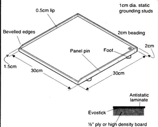
Fig.47 Construction of a small SM workstation lcm dia. static 0.5-cm lip grounding
studs Beveled edges 2 cm beading Antistatic laminate Egoistic 1/2" ply
or high density board
To construct this, prepare the baseboard from, ideally, high density chipboard or half inch plywood. Get it all squared up so that there will be no gaps at the side. Apply a layer of antistatic laminate, if you can get hold of it. I find a light green color to be the best for SM, the grey shade is the same color as some C0G chip caps and does not improve visibility. This material has a surface resistance of 108 ohms per square. It is referred to as static dissipative, as it will disperse charge but will not short out a working circuit. A 10 mm press stud placed at the top right hand corner will allow a ground connection and a wrist strap connection if you are working with expensive static sensitive devices. The laminate is bonded to the base board with standard contact adhesive.
Coat both surfaces and let them dry for 30 minutes. Then put them together, you've got to get this right first time because once contacted it won't move. Allow for slight misalignment and plane back to the baseboard to get a square edge. Now apply the beading which should be neatly cut and sanded. Make fancy joints if you can, but simple butt joints are adequate.
Plane down the front piece to give just a small retaining wall and chamfer the sides to meet it. Long panel pins are adequate to hold the sides but chipboard screws give a more secure job if a small pilot hole is drilled first. Four rubber feet near the corners will allow the work station to sit securely on the bench without rocking. Finally paint it with clear varnish taking care not to get any on the antistatic surface. The laminate can be maintained and kept clean with proprietary antistatic cleaner.
3. Chip Control
Having produced our protected work area let's home in on the final assault on the live wire detector project in more detail.
Placing a 1206 chip resistor on its solder pads will soon reveal the need for some control over the thing. The slightest movement of the PCB knocks it out of place. If you try to solder one end without holding it down it will do some strange things. As the solder wets the end of the chip it will be pulled into the center of the solder blob or in some cases it will stand on end. This latter effect is known as "tombstoning". It has other pet names like the Stonehenge effect, the Manhattan effect and draw-bridging. The effect is most prevalent in production situations using solder paste but the cause is the same. When the end of the chip is wet by the solder the surface tension is sufficient to pull it into the vertical position. The density of an SMD is much lower than lead based solder so it floats on the molten pool.
Since only one end is wet and the surface tension pulls it in all directions it moves to equalize the forces by tombstoning. This is illustrated in Figure 48.
The effects of surface tension are not all bad. Surface tension forces are involved with the very important process of spreading and wetting. In reflow soldering the chips float into alignment with the solder pads as a result of surface tension.
Similarly self alignment of chips on solder-masked PCBs is a surface tension effect. To avoid tombstoning and because of the light weight of chip components it is essential to hold them in place whilst hand soldering. The simplest method is to nudge the chip into the required position with a toothpick and then pin it down with same whilst one end is soldered. The toothpick, being made of wood, does not slip on the surface of the component as the hard point of a pair of tweezers might. This is the anchor-one-end method and it works quite well but after soldering the free end it is sometimes necessary to re-solder the anchor end to get a good joint. This subjects the SMD to more thermal stress and often excessive solder loading into the joint.
It is therefore not the best soldering technique in that it is difficult to solder correctly in this way. To do the job right one hand holds the chip down, one hand holds the soldering iron and another hand must hold the solder wire so that it can be applied to the joint at the same time as the iron tip. This way the whole joint is rapidly enveloped with oxide beating flux. This is the correct way to solder and requires three hands. You haven't got three hands! Putting solder on the iron and carrying it to the joint is bad because the flux vaporizes in the second it takes to get there. Without a protecting coat of flux the solder arriving at the pad is already oxidizing at the high temperature and becomes a poor wetter. Molecular layers of oxide already on the copper tracking and on the chip ends have no acidic flux to dislodge them. The incoming solder rests on the surfaces and a dry or unsound joint results. Therefore a device is required to hold the chip in place whilst applying the iron with one hand and the solder with the other. This requires two hands. You have got two hands. I have seen many designs for SMD assembly jigs but the one shown in Figure 49 is very satisfactory.
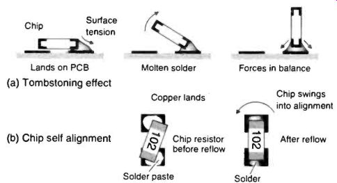
Fig.48 Surface tension effects encountered during reflow soldering---Lands
on PCB (a) Tombstoning effect; Molten solder; Forces in balance; Copper lands;
Chip swings into alignment (b) Chip self alignment; Chip resistor before
reflow; After reflow; Solder paste; Solder
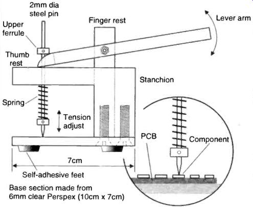
Fig.49 A well designed SMD assembly jig
This was developed for professional prototyping laboratories and educational establishments and is a real help to the amateur constructor. It will take PCBs up to several centimeters and is ideal for most SM projects. Splitting a large project into smaller functional units has many advantages. This will also help in the unlikely event that you run out of jig capacity. To use this little jig the PCB is placed in it with the target solder pads under the retaining pin. This pin is lightly spring loaded and is machined to a flattened point about 0.5mm diameter. A thumb placed on the thumb rest will steady the jig which is quite small and light, whilst the lever arm is operated with the fingers. The chip component is placed under the pin with a pair of tweezers and is held firmly in place by the pin on releasing the lever arm.
The chip can be partly released to allow it to be nicely aligned using the tweezers. To lubricate the pin a non-silicone grease gives much smoother operation, particularly if Perspex is used as a construction material. The jig has other uses: it's a good way of holding a circuit whilst working on it, adding Kynar wire links, testing, and so on. I cannot recommend this little assembly jig too strongly. It makes SM work so much easier and once you have tried it you will wonder how you managed without it.
----------
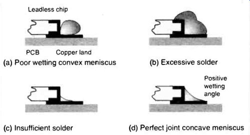
Fig.50 The perfect SM soldered joint: Leadless chip , PCB Copper land (a) Poor
wetting convex meniscus (c) Insufficient solder (b) Excessive solder Positive
wetting angle (d) Perfect joint concave meniscus
-----------
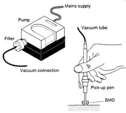
Fig.51 An effective vacuum pick-up system
----------
4. The Perfect Joint
Having the capability to solder, you can concentrate on making the perfect joint. The preparation of a flux coated PCB has been mentioned. A PCB prepared in this way has a high surface friction coefficient and it will be easier to control the chips even with the jig. The finer solder wires are a bit lacking in flux con tent and the extra flux on the PCB comes in handy. If all is clean and ready with the chip in control in the jig, apply a clean and well tinned iron tip to the solder pad, not the component. After an almost imperceptible delay of about half a second touch the pad close to the iron tip with the solder wire and remove almost instantly. Keep the iron in place and let the solder spread out wetting the chip contact area. Finally remove the iron tip. The complete operation should take less than 3 seconds. The solder loading should look like Figure 50(d). In practice it is more likely that excessive solder will be added rather than too little.
Use your big magnifier to observe the action at close quarters.
Excess solder in the joint results from leaving the solder wire in contact for too long. This may seem obvious but such a small quantity of solder is required that some skill has to be developed to just touch the joint for the very short time needed.
The other reason for excess solder loading is the result of poor solderability when more and more solder is pushed into the joint until finally wetting occurs. Here the need is really for more flux, but this comes with the solder and so more wire is pushed onto the job. A quick spray with rework flux from an aerosol or flux paste from a syringe will often sort matters out.
Excess solder should be removed with solder wick. If you shop around you will find specially fine wick designed for SM work.
When population is complete clean excessive flux, and other deposits, from the circuit with PCB cleaner and apply a protective solder-through coating. Following the advice above should lead you to a neat implementation of the audio amplifier.
5. More Gadgets
Another gadget which is popular with SMDers is the vacuum pick-up pen. Industrial automatic pick and place machines use a small vacuum nozzle, turning the vacuum on and off to pick up and release the chip. Such machines are computer controlled and the chips can be placed very accurately in preprogrammed positions. Hand operated vacuum pens are readily available.
The simplest types have a manual suction bulb and they represent the lowest cost approach. The more expensive types have a vacuum pump, not unlike a fish tank air pump and these are very useful indeed. The vacuum is controlled by the forefinger on a small hole. They come into their own if several components are to be placed on a PCB ready for reflow soldering with solder paste. This device is excellent for sorting or counting of SMDs. Vacuum tweezers are better for picking up larger ICs than ordinary tweezers. Tiny rubber sucker attachments are available for this purpose. They also have uses in rework operations which will be discussed later. An example is shown in Figure 51. The in-line filter will protect the pump from flux residues which can damage the rubber in the pump.
When you are completing a project, prototyping or designing a PCB layout it is very convenient to have several common components within easy reach and possibly an SMD junk box.
There is ample room on the work station to store several SMDs if suitable small containers can be found. Some ingenuity is required here and one solution comes from biochemical laboratory suppliers in the form of multi-well test chambers. These make a great bench-tidy or junk box. Typically they contain several flat bottomed wells under lcm in diameter. This is large enough to pick chips out with a pair of non-curved tweezers.
One particular sample measures 12.8cm by 8.5cm and contains 96 wells. They are very stable and won't easily topple over. In one of these you can store a full set of E12 resistors or capacitors with many wells to spare for discrete devices or junk components. Remember that chip capacitors are not marked so if you drop one into the wrong well, well! A soft sponge-rubber plug stuffed into each chamber with your tweezers will act as a good stopper. Test for a rubber that's smooth and doesn't pull the chips out with it. This type of bench tidy is illustrated in Figure 52.
Fig.52 A useful bench-tidy for SM chips
Inter-wiring SM modules and on-PCB links can soon become unwieldy with normal hook-up wire. This type of wire requires contact pads which are out of proportion to the whole design and a waste of space, besides looking unsightly. The ideal wire to use for SM work is single core (1/0.25mm) Kynar wirewrap wire. It is solid silver plated and has excellent solder ability. The thin Kynar insulation (300V) strips cleanly and easily without stretching. The small side cutters offered for SM work are very sharp and will do this for you. An important feature is the lack of melting back during soldering. A variety of colors is a great help. Where a flexible connection is required look around for some fine multistrand wire and miniature SM connectors.
Summarizing this section, a good set-up for population and commissioning of an SM project will boast several gadgets which together make the practice a great pleasure and the results a work of art to be proud of. An example of a basic set-up is shown in Figure 53. Soldering iron, re-work bits and other support hardware can be conveniently placed close to the work station.
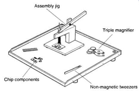
Fig.53 A workstation set-up for small SM projects-- Assembly jig Chip components;
Triple magnifier; Non-magnetic tweezers