AMAZON multi-meters discounts AMAZON oscilloscope discounts
Passing the component-level low energy ESD (CDM, MM, HBM) standard ESD tests don’t guarantee withstanding of high energy ESD transients introduced by the system-level ESD pulses up to 30 kV in the field application that could impact real products reliability. The most common test methodology to validate the ESD immunity (susceptibility) of the products is IEC 61000-4-2 [8]. It defines the ESD pulse waveform, voltage/current values, test conditions and procedures. The standard is discussed in detail in the following Sect. 2.
The trend towards smaller form factors of the systems is propagated to the IC product specifications and further supported by scaling of the semiconductor processes down to the advanced technology nodes both for active devices and inter connects. The implementation of the power optimized high-speed circuits that brings overall more susceptibility and damages at already low ESD stress levels.
Under those conditions the on-chip protection design for system-level ESD stress becomes increasingly challenging. For many cases the off-chip protection becomes a more cost effective approach. A detailed off-chip protection overview is described in Sect. 5. In this introductory section some material towards an overall off-chip ESD protection strategy is provided to help further understanding of the on-chip and off-chip ESD protection aspects discussed in the following Sects. 2 3 and 4.
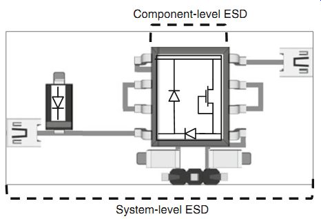
Fgr. 20 Illustration of building blocks in a system on a chip.
Trend Toward High Level Integration: SoC and SiP
The trend towards high level of the system functional blocks integration on-chip resulted in removing the barrier between the components and systems. System- on-chip (SoC) and system-in-package (SiP) designs now can combine a variety of analog and digital circuit blocks that directly interface with system ports. The trend is supported by emerging manufacturing options like the 2.5D and 3D packaging techniques. This creates a significant paradigm shift and in particular results in the definition of system-levels ESD passing specifications for selected IC pins.
This trend requires the implementation and integration of different ESD design strategies for RF, high-voltage analog, and low voltage digital circuits on the same die or in the same IC package. While the majority of the SoC or SiP IC pins are still required to pass only component-level ESD specifications, the presence of the pins with system-level requirements significantly impacts the overall ESD design strategy. This is mainly because of the possible interaction of the IC blocks.
Many of the SoCs are used in handheld and mobile devices like smart phones and tablet computer. Next to the central processing unit (CPU) and memory controller interfaces like USB and flash memory, the power management, display and sensor ICs and the radio for wireless communication are integrated in one IC ( Fgr. 20). The challenge of predicting the system-level ESD robustness of an IC before it’s mounted in a system is combined with the trend to minimize the number of (off-chip) components in an application board. As a result IC suppliers are expected to deliver system-level ESD robustness without a detailed knowledge of the final application board, block or system design. At the same time the system designers expect a more robust component (IC)-level ESD protection to ensure higher system-level ESD robustness.
ESD Voltage Suppression
Fgr. 21 Concept of system-level and component level ESD protection design:
example of an application board with IC, decoupling network, off-chip ESD protection
and connectors
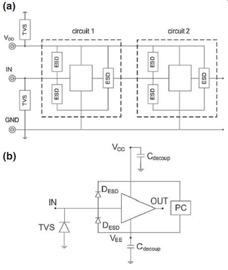
Fgr. 22 Illustration of the system-level ESD protection design concept for
TVS system-level off-chip ESD protection of two circuits (a) and a buffer amplifier
(b)
ESD protection components, while the secondary network components are rep resented by either on PCB passive or on-chip active components ( Fgr. 21).
Off-chip protection can involve numerous options including isolation and filtering circuits and transient voltage suppressor (TVS) components. The variety of the suppression components includes multilayer varistors, silicon diodes or polymer-based suppressors.
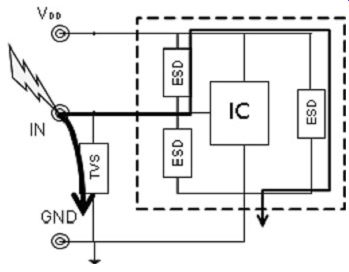
Fgr. 23 Illustration for the current path in case of ESD stress at the system-level
pin
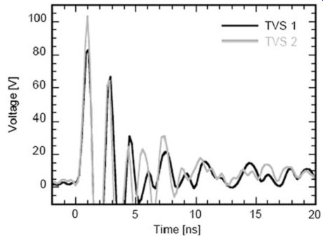
Fgr. 24 Voltage waveform during IEC 61000-4-2 stress of two different TVS
diodes.
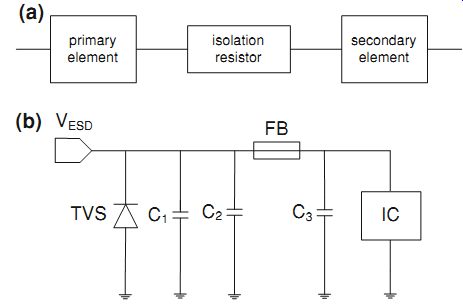
Fgr. 25 Illustration of the multi-stage ESD protection concept for the off-chip
with the second stage resistor (a) and ferrite bead (b)
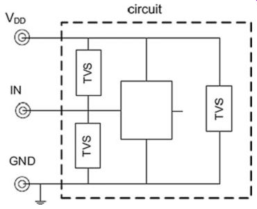
Fgr. 26 Illustration for the implementation of system level ESD protection
on-chip
From cost and performance perspective the number of ESD protection components on board of system-level must be reduced. Thus, a logical approach is the on-chip implementation of system-level ESD protection structures (Fgr. 26).
The trade-off between the off- and on- chip ESD protection strategies is related to the required on-chip area versus the cost of the PCB components assembly.
The latter is the major cost component since typically the cost of the discrete components itself is rather low. An ESD clamp with an intrinsic current capability of 5 mA/um and passing 2 kV HBM in assumption of linear width scaling must be designed at least 13 times wider to be able to pass 8 kV IEC 61000-4-2 stress. In addition to the larger ESD clamp size also the metal routing needs to be improved to carry safely the high system-level ESD stress current to the protection device.
The larger device and metal area goes along with a significant increase of the overall parasitic capacitance. This aspect is discussed more in the following section.
In more details the on-chip design for the system-level pins from the protection devices perspective is described in Sect. 3. The system-level ESD protection for external IC pins with on-chip and off-chip protection devices is addressed in the Sect. 5.
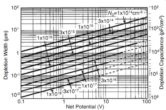
Fgr. 27 Depletion-layer width and depletion-layer capacitance per unit area
as a function of net potential for one-sided abrupt junctions in Si; doping
N is from the lightly doped side; dashed lines represent breakdown conditions
[9]
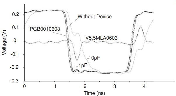
Fgr. 28 Signal response waveforms of different devices and capacitors at
USB 2.0 High Speed at peak to peak voltage amplitude 480 mV and signal frequency
at 480 Mbit/s from data [10]
Capacitance and Signal Integrity
In the past ESD energy has been traditionally shunted away from the IC pins using devices with equivalent capacitances of ~10-100 pF. Due to the trend towards higher signal frequencies this parasitic capacitance level unfortunately introduces a significant signal distortion. At the same time modern high speed data ports can only tolerate a very limited increase of the line capacitance allocated for ESD protection devices.
Implementation of the integrated on-chip ESD protection devices with a pulsed current carrying capability of over 30 Amps and less than 1 pF equivalent capacitance often is simply incompatible with the integrated process technology.
Indeed, to achieve a low equivalent capacitance the blocking junction requires the incorporation of a rather large depletion region. For example to achieve a system level ESD robustness for an asymmetrical p-n junction with the 0.1 pF capacitance and 5 V breakdown, the diode requires an isolated n-region of ~8 lm with the doping level of ~1-15 cm-3 ( Fgr. 27).
This combination of parameters is hard to find in integrated processes, especially, if substrate isolation is required. Therefore for high data rate system-level protection the main off-chip protection approach includes a discrete off-chip suppressor with optimized characteristics based on its vertical device architecture.
For low signal frequencies the overall implementation of the protection with the suppressor can utilize a separation between the signal frequency domain and any undesired frequencies domains like EMI and ESD transient pulses. Thus the TVS capacitance still enables filtering by forming a low band pass filter with the PCB trace inductance. In this case the suppressor provides both the clamping functions for transient suppression and simultaneously EMI noise filtering against unwanted, high-frequency signals that couple into the protected data line. For example the headset terminals on a cell phone operate at relatively low audio frequency, while the ESD and the cell phone operating frequencies (0.8-1.9 GHz) are much higher.
For these applications a high capacitance TVS can be a more appropriate choice to provide system-level ESD protection by the filtering out the radiated cell phone signals from the headset lines.
However, the advantages of low pass filtering are vanishing when the signal data rate is high. The high-speed data lines include the USB2.0, IEEE 1394, Gigabit Ethernet, and Infiniband protocols, etc. The data rates of all these protocols exceed 100 Mbps to guarantee a high throughput for video, audio, and data signals. The corresponding wide bandwidth of the transmission line cannot tolerate high TVS capacitances used for filtering, since the side-effect is a filtering of the data signals themselves or distortion of data waveforms causing system inoperability.
The distortion is realized in form of rounding leading and trailing edges of high/ low state transitions due to slower rise and fall times. The slower rise/fall times introduce timing issues in the circuit functionality mixing the expected ''high'' and ''low'' states at the specific times. With the signal components degradation, the ability of the circuit to recognize the intended information is decreased making it much harder to maintain the data signal integrity. Therefore over recent years a number of low parasitic capacitance TVS components with the equivalent capacitance ~0.1 pF have been developed and released by many industry leading TVS production companies.
An example of the signal distortion by the discrete active and passive components in case TVS devices and ceramic capacitors is presented in Fgr. 28 for the suppressor with 0.05 pF, ML ceramic capacitor of 1 pF, ML ceramic capacitor of 10 pF and multilayer varistor of 660 pF [10].
For the 480 Mb/s data rate the 660 pF varistor capacitance causes a distortion that completely prevents the reaching of the signal operating voltage. Even the capacitance value of 10 pF is high enough to cause substantial distortion to the waveform, the decrease in the amount of level time and significant changes in the leading and trailing edge shapes. The capacitance value of 1 pF shows a small amount of edge distortion, while the 0.05 pF capacitance value allows the data waveform to pass without distortion. The rise time (10/90 %) data for each capacitance value for the bit rate of 480 Mbps demonstrate the corresponding effect [10]. For the measurement setup with either no devices or 0.05 pF Suppressor 10/90 % rise time was at 225 ps, while ceramic SMD capacitors of 1 and 10 pF impacted the rise time up to 275 and 526 ps, respectively. Thus the capacitance characteristic of an ESD suppressor is extremely important when protecting high speed data lines to maintain the integrity of high-speed data signals.
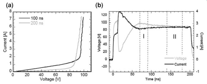
Fgr. 29 TLP I-V characteristics (a) and 200 ns TLP voltage and current waveforms
of varistor S10k40 for the stress level 120 V with marked measurements windows
I and II (b)
ESD Suppressor Considerations for Off-Chip Network
In addition to the two major factors, the clamping voltage waveforms and the capacitance realized in the off-chip ESD protection network with transient voltage suppressors (TVS), a number of other important considerations must be taken into account.
Some aspects of TVS device design are discussed in Sect. 3 and their application for co-design in Sect. 5. The majority of TVS components can be subdivided into three categories: polymer, varistor, and semiconductor diode suppressors. The polymer suppressor diodes are based upon tunneling and breakdown conductivity modulation effects between conductive nano-particles introduced into the polymer. They provide an advantage in extremely low parasitic capacitance, but cannot limit voltage at low level. The varistors (or voltage variable resistors) have different designs. Most of them are zinc oxide metal-oxide varistors. The varistor operation principle is based upon the combination of thermo-ionic emission and electron tunneling. The varistors are usually effective to protect against very strong ESD events-- for example street lights against lightning strike. For the semiconductor systems the disadvantage of varistors is their high capacitance and low amount of zaps they can withstand. Similar to polymer suppressors the varistors clamping voltage is usually rather high.
For example varistors are made of metal electrodes and Zinc-oxide (ZnO) ceramic layers. ZnO grains on the ceramic layer form diode-like junctions which allow the flow of current only in one direction. During normal circuit operation the varistor is off. The capacitance of a varistor is typically rather high due to the large amount of junctions. The varistor starts conducting if during ESD stress the breakdown voltage of the varistor is exceeded. The current conduction spreads uniformly throughout the varistor which allows a very high robustness also to surge currents. According to TLP characteristics the positive feedback in the device does not provide S-shape I-V characteristics ( Fgr. 29a) [5].
The clamping voltage in the I-V characteristics of the varistor varies with the TLP stress duration is due relatively slow turn-on ( Fgr. 29b). After a TLP stress of 100 ns the varistor is not reaching the quasi-static state. The large capacitance varistors have a rather poor long-term reliability. After a few ESD zaps varistors degradation can be noticed in form of an increased off-state leakage current.
Another alternative solution-spark gap is usually composed by two electrodes with a certain distance to each other. This ''gap'' is filled with air or another gas that allows sparking between the two electrodes. When the (usually very high) breakdown voltage is exceeded, the gas in between the electrodes becomes ionized creating an arc discharge with low resistance. In addition to the high breakdown voltage the spark gap needs a certain time for the ionization of the air or gas used.
This delays the breakdown or triggering of the spark gap. Ones triggered, spark gaps show a ''snapback-like'' behavior with a very low clamping voltage. The use of spark gaps and varistors can be justified mainly for high voltage application with several hundreds of volts tolerance.
Similar characteristics are delivered by polymer voltage suppressor (PVS) devices. The principle design is somewhat similar to a spark gap with the discharge realization in a polymeric material instead of air. The polymer material has a very low dielectric constant which results in a capacitance below 200 pF for a device in SMD0603 form factor. However the main drawback is related to high triggering and clamping voltages above 100 V.
Passive board-level components were historically used as primary current path components in system-level ESD protection. Two commonly used devices are capacitors and ferrite beads. Both devices are able to either conduct or block the ESD current by filtering.
A capacitor in parallel to an IC pin conducts large part of the ESD current under very low clamping voltage. However, all discrete capacitors have metal electrodes and pins with a parasitic inductance. An inductance of a few nH may be present depending on the length of the connector pins and the design of the capacitor case.
The capacitor parasitic can cause an unwanted voltage drop across the ESD device during the fast rising edge of ESD currents. These voltage peaks must be taken into account when using a capacitor as an ESD protection device in parallel to an IC.
Ferrite beads are passive devices that represent a functionality similar to a band pass filter. Depending on the ferrite bead model, either the lower frequency or the higher frequency components of the ESD current are filtered. Ferrite beads are used in series to the protected pin. Depending on the model, a ferrite bead can suffer from saturation at large stress currents thus limiting its suitability for ESD protection.
=====
Table 3 Overview on electrical parameter of common system-level ESD protection devices RON (X)VBD (V) Vclamp (V) C (pF) tON (ns) TVS diodes \1 [3 [10 [2 \1 1 … 1.5 [3 [10 \2 \1 Varistors [20 [30 [100 [2 \40 [20 [50 [200 \2 \40 Polymers \1 [250 [200 \0.1 [5 Capacitors _1 Full range \1
======
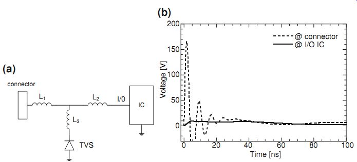
Fgr. 30 Simplified block diagram for protection with TVS on PCB (a) and corresponding
voltage waveforms measured at TVS and I/O nodes (b)
==========
Table 3 summarizes the electrical parameters of the devices that can be used for off-chip system-level ESD protection with the parameters: RON: on-resistance, VBD: DC breakdown voltage (at current I = 1 mA), V_clamp: clamping voltage after 30 ns @ 8 kV IEC 61000-4-2, tON: turn-on time, C: at 1 MHz. TVS diodes trigger at low breakdown voltages and are available with comparable low parasitic capacitance. This makes them the most suitable candidates for the system-level ESD protection for low-voltage and high-speed applications. For analog and high voltage applications high-breakdown TVS diodes, varistors and capacitors represent the most suitable off-chip protection devices.
When a TVS is chosen for appropriate suppression level and other electrical characteristics including a good match with the system circuit parameters, the remaining design steps include the choice of the on-board TVS location for most optimal performance to take advantage of the parasitic inductance of the PCB traces.
Similar to capacitance, low frequency signals will be unaffected by the inductance that is presented by the board traces. However, at high frequencies, the inductance will be present as an impedance component that can affect signal integrity: RL = xL. Even a relatively short trace inductance can provide rather high impedance if the frequency is high enough. Therefore the more distance is between the ESD suppressor and the protected chip pin on PCB the lower is the voltage at the pin. In the diagram ( Fgr. 30a) the inductance L1 physically represents a connection between the port and the ESD suppressor; L2-between the ESD suppressor and the I/O pin of the chip, L3-between the I/O line and the ESD suppressor. This strategy provides a significant suppression of the voltage wave form at the IC pin ( Fgr. 30b).
The inductance L2 provides attenuation of the ESD pulse voltage and current as the energy is stored and dissipated in the electromagnetic field around the board trace. The attenuation of the ESD pulse propagates down the board trace. Thus the TVS placement location is favorable to be installed at a connector which is usually one entry point for ESD transients.
In the case ( Fgr. 30) a TVS is chosen with a rather high voltage overshoot and clamping voltage. The waveform at the suppressor for the 1 kV TLP pulse at the connector has the measured peak voltage ~350 V and the holding voltage of 75V.
It’s clear that a voltage of 650 V at a PCB trace may create a substantial coupling at high frequency. If a 3-inch long trace (L2) is connected to the ESD suppressor site and the input pad for the IC the attenuation of the overshoot peak voltage is ~6 times and ''clamping'' voltage is reduced from ~60 V to approximately 25 V. The reduction corresponds to the frequency dependent impedance of the PCB line L2.
By increasing the trace length between the ESD suppressor and the chip the stress at the IC pin can be dramatically reduced. The ESD suppressor should be located directly behind the connector. It should be the first board-level component that the ESD transient encounters.
Extrapolating this empirical analysis the optimal location can be derived as follows:
(i) Inside connectors to the system shielding (chassis), (ii) At the point where circuit board traces interact with the connector pins, (iii) On the circuit board immediately behind the connector, (iv) On robust, unprotected lines that may efficiently couple to I/O lines, (v) Before a series resistive element on a data line, (vi) Before a fan-out point on a data line, (vii) Near the IC pin.
Another placement consideration is the distance from the board data signal trace to the TVS itself represented by the inductance L3 ( Fgr. 29). This trace inductance should be minimized to reduce the voltage drop in the signal line cross point of the circuit where all inductors are connected. If the L3 is high the TVS becomes isolated from the signal line by the inductance impedance. Thus the ideal placement for the TVS solder pad is on top of the data line trace.
Respectively the chassis or frame ground is expected to work as ESDMINUS bus. To avoid the coupling the ESD stress signal with the data signal two different current paths implemented by design is the most optimal approach. By referencing the TVS to the chassis ground, unintentional noise effects and ground bounce can be reduced to maintain signal integrity.
The most useful suppressors that started to dominate over recent year for portable semiconductor systems are based on Si material. The design is somewhat similar to other on-chip ESD devices combining the precise breakdown characteristics and high performance with multiport integration. However most of the design advantages can be taken from the discrete approach using vertical device architecture supported by the dedicated process technology.
The comparison of the ESD protection devices using only data sheet parameters with ESD level ratings and cost is not always optimal. For example, device "A" may have in its datasheet a level of IEC 61000-4-2 robustness ~5 kV, while device "B" can guarantee ~20 kV. However this range represents only the level of survivability of the TVS devices rather than a diode clamping waveform characteristic. If device ''A'' provides a more appropriate ESD operation wave form the system design can be substantially better rather than when using device ''B''. At the same PCB trace connection the waveforms realized at the TVS connection will determine the magnitude of the secondary current through the IC pin.
Unless provided in the datasheet, the clamping voltage and residual current estimation in the ESD time domain may not be simple. The clamping voltage parameter in the suppressor datasheets, if it’s present at all, might be misleading, since it can only indicate the clamping voltage after the voltage overshoot at the beginning of the ESD pulse. At the same time the residual current can be only calculated based on the PCB trace design.
Polymer based TVS seem to be attractive for high-frequency applications due to their low capacitance of 0.05-1.0 pF. However, they usually have triggering voltages that are significantly higher than the clamping voltage. A typical polymeric suppressor breakdown is around 300-500 V with a clamping voltage after the snap back of up to 150 V. In addition polymer suppressor may have a very long recovery time up to a few hours of even a day to transit to the high-impedance state after the ESD pulse.
Varistor type suppressors are low cost, but have too high triggering and clamping voltages, as well as a high resistance. Typical low capacitance varistor TVS have the clamping voltages range 150-500 V and a dynamic resistance of above 20 X. Another side effect is the possible degradation with multiple stresses.
Most varistors can reversibly operate for 10-20 zaps only.
The most optimal method used for systems ESD protection is based upon the semiconductor TVS diodes. ESD protection diodes are characterized by low clamping voltages, low resistance, fast turn-on times, and good ESD reliability. In general, semiconductor diodes offer the best ESD protection, and now available with capacitances below 0.1-1 pF to guarantee a good signal integrity.
Current industry practice is to publish clamping voltages based on a pulse with an 8 uS rise time and duration of 20 uS. This is the specification for the power surge rather than ESD event. Most datasheets document clamping voltage using a 1 A pulse and sometimes a higher current pulse as well. This pulse is not equivalent to a fast transient ESD system level pulse with below 1 ns rise time and duration of 100-150 ns. The TVS clamping voltage during a level 4 IEC 61000-4-2 pulse with a peak current of ~30 Amps is in general different from the microsecond time domain at 1-3 A surge current provided in the TVS datasheet. Thus the IC-system co-design methodologies involve additional pulsed characterization (Sect. 5) In general, semiconductor diodes deliver the lowest peak clamping voltages, while suppressors and polymers have significantly higher clamping voltage characteristics. Typically the low voltage semiconductor TVS diodes are rated to clamp the voltage at the level of 8-15 V range for 8 kV IEC 61000-4-2 stress. This is achieved in significant contrast with varistor and polymer suppressors that can have clamping voltages in the range of 150-500 V. Consequently the secondary current through the IC pin depends on the dynamic resistance of the entire off-chip network with the voltage limited by a TVS placed at the system port.
There are various options available for ESD protection with Si suppressor devices: SCR diodes, TVS Avalanche diodes and punch-through BJT devices. The board level ESD protection design varies from system to system. Factors that influence the design include board layout, the ESD capabilities of the IC, and the physical ability of ESD transients to get on the data lines. Empirical testing can also be done to deter mine the system's susceptibility. If it’s determined that a supplemental ESD protection is desired, the next step is to identify the appropriate suppressor. There are many characteristics that should be considered including: capacitance, peak and clamping level, leakage current and the system operating voltage.
Another consideration is the number of lines to be protected. This is determined by the system's data protocol. For example, USB buses have two data lines, RS 485 uses two lines per differential pair, 10/100BaseT Ethernet uses four lines, etc.
In cases where multiple data lines are protected, it may be desirable to use a multi port suppressor to save board space and assembling costs.
Recognizing that a radically new approach is required to meet today's ESD requirements a number of companies has introduced the new Si TVS architecture getting significantly better ESD performance than traditional off-chip ESD protection devices.
Top of page Article Index HOME